New Intra-Body Sensor for
E-Health Applications
June 2010
New Intra-Body Sensor for
E-Health Applications
DISSERTATION
submitted to University of Beira Interior in partial fulfillment of the requirement for the degree of
MASTER OF SCIENCE
in
INFORMATION SYSTEMS AND TECHNOLOGIES by
João Filipe Roxo Garcia
Department of Informatics University of Beira Interior
Covilhã, Portugal http://www.di.ubi.pt
Copyright 2009 by João Filipe Roxo Garcia. All right reserved. No part of this
publication can be reproduced, stored in a retrieval system, or transmitted, in any form or by any means, electronic, mechanical, photocopying, recording, or otherwise, without the previous written permission of the author.
i
New Intra-Body Sensor for
E-Health Applications
Author: João Filipe Roxo Garcia Student nº: m3024
Email: jfr.garcia@gmail.com
Abstract
Sensor nodes are small devices able to collect and retrieve sensorial data. The use of these sensors for medical purposes offers valuable contributions to improve patients‟ healthcare, both for diagnosis and therapeutics monitoring. An important and common parameter used in healthcare diagnosis is body temperature. It is monitored on several matters related with gynaecological and obstetrics issues but, usually it is measured at the skin‟s surface. Thus, this dissertation proposes the design concepts of a new intra-body sensor for long-term intra-vaginal temperature collection. The embedded IEEE 802.15.4 communication module allows the integration of this sensor in wireless sensor networks for remote data access and monitoring. It is presented the sensor architecture, the construction of the corresponding testbed, and its performance evaluation. This sensor may be used in several applications, including fertile and ovulation period detection, and preterm labor prevention. The features of the constructed testbed were validated in laboratory field verifying their accuracy and performance.
Jury:
Chair: Prof. Pedro José Guerra Araújo, FE-DI, UBI Covilhã Referee: Prof. Beatriz Sainz de Abajo, UVa, Valladolid, Spain Supervisor: Prof. Joel J. P. C. Rodrigues, FE-DI, UBI Covilhã
iii
Resumo
Os sensores são pequenos dispositivos capazes de adquirir e enviar dados. A utilização de sensores na área médica e em biofeedback oferece um contributo importante para a melhoria de cuidados de saúde, tanto ao nível diagnóstico como terapêutico.
A temperatura é um dos parâmetros mais comuns e importantes no diagnóstico médico. A sua aquisição é igualmente importante na área da ginecologia e da obstetrícia, sendo normalmente medida através da superfície da pele. Pode ser utilizada para detecção e monitorização do período de ovulação e prevenção do parto pré-termo. Por estas razões, foi construído um protótipo de um sensor intra-corporal para a aquisição e monitorização da temperatura vaginal. Porém, tendo em conta as dimensões desse protótipo, identificou-se a necessidade de construir um novo sensor que com as mesmas tecnologias e electrónica, tenha as dimensões e a forma de um vulgar tampão.
Para a construção do novo sensor foi necessário incluir um módulo de comunicação IEEE 802.15.4 para integração do sensor numa rede de sensores sem fios e sua monitorização e acesso a dados remotamente.
Nesta dissertação é apresentado o projecto, a arquitectura do sensor, a construção do protótipo e a respectiva avaliação do desempenho. O protótipo e as suas funcionalidades foram testados em ambiente laboratorial validando a sua precisão e desempenho.
v
Resumen
Los sensores son pequeños dispositivos capaces de recibir y enviar datos. La utilización de los mismos en el campo de la medicina puede contribuir a la mejora de la calidad de vida de los pacientes, tanto desde el punto de vista diagnóstico como terapeútico.
La medición de la temperatura corporal es uno de los parámetros fundamentales en un diagnóstico médico. En especialidades como ginecología y obstreticia, la medición de la temperatura corporal es empleada para la detección y monitorización del periodo de ovulación, y para la prevención de un parto prematuro. Por estas razones, se construyó un prototipo de sensor intra-corporal para la adquisión y monitorización de la temperatura vaginal. Sin embargo, dadas las dimensiones de este prototipo, se identificó la necesidad de construir un nuevo sensor empleando las mismas tecnologías y electrónica, pero con las dimensiones y la forma de un “tampón” común.
Para la construcción del nuevo sensor fue necesario incorporar un módulo de comunicación basado en el protocolo IEEE 802.15.4 para la integración de dicho sensor en una red de sensores wireless, y llevar a cabo la monitorización y acceso a los datos de forma remota.
En este proyecto se muestra la arquitectura del prototipo del nuevo sensor intra-vaginal, la construcción y evaluación funcional del mismo. El prototipo fue validado en el laboratorio con el fin de comprobar su funcionamiento y precisión.
vii
Acknowledgements
This is for sure the easiest and hardest chapter of my dissertation. It will be easy to name all the people that contributed to get this done, but not enough to show them my gratitude. I will try...
First of all, I must congratulate my supervisor Professor Joel José Puga Coelho Rodrigues for his guidance, expertise, encouragement and enormous support. For guiding me through the writing of the dissertation, and for all the corrections and revisions made to the text that is about to be read.
I am most grateful to the University of Beira Interior and the Instituto de Telecomunicações – Covilhã Delegation, especially to Next Generation Networks And Applications Group (NetGNA), Portugal, in the framework of Project BodySens and all my colleagues for many the kinds of support that was given to me. Special thanks to João Caldeira for being always thoughtful and helpful.
My final words go to my family, mother, father and brother, and close friends for their love, support, encouragement, effort and patience.
João Garcia Covilhã, Portugal June, 2010
ix
Keywords
xi
Palavras-chave
Sensores Corporais/Biossensores, Saúde Electrónica, Monitorização de Temperatura, Protótipo.
xiii
Contents
Acknowledgements ... vii Keywords ... ix Palavras-chave ... xi Contents ... xiii List of Figures ...xvList of Tables ... xvii
Acronyms and Abbreviations ... xix
1. Introduction ...1 1.1. Focus ... 1 1.2. Objectives ... 2 1.3. Motivation ... 2 1.4. Main Contributions ... 3 1.5. Dissertation Structure ... 3
2. Intra-Body Sensors and Networks ...5
2.1. Body Sensor Networks... 5
2.2. Body Sensors and Intra-Body Sensors ... 7
3. System Requirements and Architecture ...13
3.1. Requirements ... 13
xiv
3.3. Testbed Architecture ... 23
4. Intra-Vaginal Temperature Biosensor ...29
4.1. Biosensor Project Design ... 29
4.1.1. Making new Libraries and Parts ... 33
4.1.2. Biosensor Board ... 35
4.2. Temperature Sensor Integration ... 37
4.3. Firmware Development ... 40
5. System Validation – Test and Results ...43
5.1. Prototype Validation ... 43 6. Conclusions ...46 6.1. Future Work ... 47 7. References...49 Appendix A ...55 Appendix B ...57 Appendix C ...59
xv
List of Figures
Figure 1. Sensor's block diagram. ... 6
Figure 2. Several Body Sensors Networks Applications. ... 7
Figure 3. Shimmer mote. ... 8
Figure 4. Eco Mote... 9
Figure 5. Tyndall module. ... 9
Figure 6. Telos module. ... 10
Figure 7. MICAz module. ... 10
Figure 8. SAND module. ... 11
Figure 9. DuoFertility module. ... 12
Figure 10. Conceptual design of the new intra-vaginal temperature monitoring sensor mote. ... 14
Figure 11. System architecture. ... 15
xvi
Figure 13. CC2420 functional blocks diagram. ... 19
Figure 14. TPS60100 functional blocks diagram. ... 21
Figure 15. MA100 physical structure. ... 22
Figure 16. Different temperature sensors behavior. ... 22 Figure 17. 450 mAh battery... 23
Figure 18. Biosensor block diagram of the proposal... 24 Figure 19. Physical testbed for temperature monitoring. ... 26 Figure 20. Altium schematic editor workspace. ... 32
Figure 21. New parts created with port pins and footprints. ... 34 Figure 22. Top layer (A), Bottom layer (B). ... 35 Figure 23. Thermistor signal acquisition circuit. ... 38
Figure 24. Biosensor firmware diagram. ... 41
Figure 25. Experimental testbed validation for temperature measurements. ... 44
Figure 26. Comparation between temperature values by testbed and temperature
xvii
List of Tables
Table 1. Antenova Impexa 2.4ghz features... 20 Table 2. Port pins and signal names ... 36 Table 3. Analogic to digital adc10 conversion values. ... 39
xix
Acronyms and Abbreviations
ºC : degree Celsius
ASCII : American Standard Code for Information Interchange A/D : Analog to Digital Converter
ACLK : Auxiliary Clock
ADC : Analog to Digital Converter
AMON : Alert Portable Telemedical Monitor Project AnEx : Analogue External Connector Breakout Board BASN : Body Area Sensor Network
BBT : Basal Body Temperature
BSN : Body Sensor Network
CD : Compact Disc
CMOS : Complementary Metal Oxide Semiconductot
cm : centimetres
COM : Serial Port Interface CPU : Central Processing Unit CRC : Cyclic Redundancy Check DAC : Digital to Analog Converter DCO : Digitally Controlled Oscillator DTC : Data Transfer Control
xx
e.g. : exempli gratia (for example) ECG : Electrocardiography
EEG : Electroencephalography
EMG : Electromyography
FIFO : First In First Out
FPGA : Field-Programmable Gate Array Gbytes : Giga Bytes (109Bytes)
GE : General Electrics
GHz : Giga Hertz (109Hertz) GUI : Graphical User Interface
I/O : Input/Output
I2C : Inter-Integrated Circuit
IDE : Integrated Development Environment
IEEE : Institute of Electrical and Electronics Engineers
IP : Internet Protocol
ISM : Industrial Scientific Medical JTAG : Joint Test Action Group Kbps : Kilo bits per second LED : Light Emitting Diode
LNA : Low Noise Amplifier
MA100 : Thermometric Biomedical Chip Thermistor
MAB : Memory Address Bus
mAh : mili-Amperes hour
MBytes : Mega Bytes (106Bytes)
MCAD : Mechanical Computer-Aided Design
MCLK : Master Clock
MDB : Memory Data Bus
MHz : Mega Hertz (106Hertz)
MOSFET : Metal Oxide Semiconductor Field Effect Transistor NTC : Negative Temperature Coefficient
xxi
PA : Power Amplifier
PDA : Personal Digital Assistant
PC : Personal Computer
PCB : Printed Circuit Board PND : Personal Navigation Device PTC : Positive Temperature Coefficient PWM : Pulse With Modulation
RAM : Random Access Memory
RF : Radio Frequency
RH : Relative Humidity
RISC : Reduced Instruction Set Computer RTD : Resistance Temperature Detectors SAND : Small Autonomous Network Device SDK : Software Development Kit
SFD : Start of Frame Delimiter
SHIMMER : Sensing Health with Intelligence Modularity, Mobility and Experimental Reusability
SIMO : Slave In Master Out
SMCLK : Sub-Main Clock
SMD : Surface-Mount Device
SOMI : Slave Out Master In SPI : Serial Peripheral Interface TinyOS : Tiny Operating System
UART : Universal Asynchronous Receiver/Transmitter USB : Universal Serial Bus
USCI : Universal Serial Communication Interface VHDL : Very High Description Language
WBSN : Wireless Body Sensor Network WLAN : Wireless Local Area Network WSN : Wireless Sensor Network
Chapter 1
1.
Introduction
1.1. Focus
The sensors networks evolve with a lot of expectations on the middle of the investigation field due to the large applicability and possibility of development, especially in the Wireless Sensor networks (WSN). Low power consumption and low data rates are the most important features for WSN applications.
A wireless sensor network consists of a group of sensors which monitors physical or environmental parameters. Within a wireless sensor network there exist three fundamental agents, the sensor node, the event and the reporter. The sensor node captures the event parameter, reads and sends the information to be studied by the reporter [1-2]. The reporter is the final user who will analyze and try to get solutions. This dissertation approaches Body Sensor Network (BSN) because all the monitored parameters are directly collected from the human body.
Actually, due to the technological evolution of e-health it‟s possible have sensors for all the sizes and a lot of features, sensors that even can be placed inside (intra-body sensor) or outside (inter-body sensor) of the human body, most of in contact with skin. All these types of sensors deal with many constrains on resources such as energy, memory, computational speed and bandwidth. Furthermore, with this evolution these
Introduction
2
platforms are very helpful for medical diagnoses and treatment methods because some of them can only be recorded by electronic sensors.
1.2.
Objectives
The main objective of this dissertation is the proposal of a new intra-body sensor for e-health applications, and its corresponding prototyping, performance evaluation, and validation. To reach the main objective, some intermediate objectives were identified and performed.
To reach this main objective the following intermediate objectives were identified and performed:
Detailed review of the related literature on intra-body sensors and studies of available hardware.
Construction of a new prototype in breadboard (testbed), to ensure temperature monitoring and the storage of data.
Design of a miniaturized/optimized biosensor to reduce patient constrains in use.
Proposal of a firmware for the new biosensor.
Test and validate the created testbed in laboratory field to simulate the same conditions of the real application.
1.3.
Motivation
All the studies based on body temperature control started earlier as a tool to detect fertility period by observing the increasing of body temperature, know by basal body temperature (BBT) taken with a basal digital thermometer [3]. This method is very painful for females and does not guarantee a successful validity of gathered data. A lot of reasons could be presented to displease this method, like accuracy of equipment,
Introduction
3 appropriate environment, and external temperature factors or misuse of equipment. Along with all of this, and the reduced biosensors available on the market to perform this task, it proved to be a great effort to develop and realize this biosensor.
Another motivation stems from the close collaboration with the medical team, which introduces great confidence on all stages of development. This work will provide a great deal of data that could be very useful for medical studies with temperature and acquisition time (day and hour).
The medical staff will establish a correlation between the intra-vaginal temperature and some stages in female reproductive system in order to prevent pregnancy issues. The medical team is well led by an expertise in this area by Prof. José A. F. Moutinho, from Health Sciences Faculty, University of Beira Interior, Covilhã, Portugal. This closed collaboration is an important contribution for medical validation of accuracy, usability, efficiency, and system performance evaluation and validation.
1.4.
Main Contributions
This section is devoted to the scientific contributions of this work project to the state-of-art in intra-body sensors.
This contribution is a major and detailed design of a new intra-body sensor for e-Health applications, specifically for temperature monitoring with wireless communication. It also presents a testbed construction and results achieved to validate the system. The paper will be presented at 5th International Conference on Body Area Networks (BodyNets 2010) [4].
1.5.
Dissertation Structure
The dissertation is organized in six chapters and the chapters are organizes as follows. This chapter, the first, presents the context of the dissertation, focusing the topic under studies, the main objectives, the dissertation structure and its motivation.
Introduction
4
Chapter 2 presents a literature review on Sensors and Body Sensor Networks, the main theme of this dissertation. This chapter begins with the description of a Body Sensor architecture being paid special attention to wireless sensor networks as explain i n Section 2.1, and Section 2.2 focuses on the body and intra body sensors and their appliance, importance for e-Health development.
In Chapter 3, the requirements, the description of the hardware for the testbed architecture proposed is described.
Chapter 4 presents the design project for the new intra-vaginal temperature biosensor. Section 4.1 explains how the new libraries and electronic component parts were made, and the description of the biosensor PCB project. This chapter contemplates two more sections; the integration of the temperature sensor is presented on the Section 4.2 and the firmware development on Section 4.3.
In Chapter 5 is presented some test performed with the testbed in order to validate the developed system.
Finally, Chapter 6 concludes the dissertation with it main research findings and puts forward proposals for further research direction.
Chapter 2
2.
Intra-Body Sensors and Networks
This chapter presents an overview of all the main areas where this work is included. It begins with an overview about body sensor networks and continues with description of some available body sensors and where they are applied.
2.1. Body Sensor Networks
A body sensor network (BSN) is a sensor network for body applications. These sensor networks are applied in medical care and biofeed-back, providing healthcare monitoring services [5]. The aim of BSN is to provide continuous monitoring of patients under their natural physiological state so that transient but life threatening abnormalities can be detected and predicted. This network is composed of a sensing node with a processing unit and limited power supply, if the sense node is provided with a wireless transceiver we are dealing with a Wireless Sensor Network [2]. The sensors nodes or motes are the main agent because they are capable of performing some processing, recording sensory information and communicating with other connected nodes in the same network. The messages from sensors in some networks are collected by the network controller and processed on a personal server or in some applications can talk directly to the Internet gateway. In body area sensor networks (BASN) [6-7] the signals collected by sensors retrieve them to the sink node which are connected to a central computer. This
Intra Body Sensors and Networks
6
computer gathers and processes all data collected from all sensors on the network to be interpreted by an expertise. The communications between sensor nodes are usually wireless technologies like Bluetooth and Zigbee [8] over IEEE 802.15.4, but the most used and better for wearable health applications is Zigbee communication due to lower power consumption [9-10].
A typical architecture of a sensor node as shown in Figure 1 is equipped with a micro-controller, a transceiver, a power source, external memory (microSD) and ADC‟s [11].
Figure 1. Sensor's block diagram.
The sensor area has a bigger development, due to fact of the industrial development on the micro electronics technology who allows the creation of smaller sensors with better processing, memory and power source.
Sensor networks could be applied in the medical environment, helping gathering fast diagnoses and providing monitoring services [5]. The concept of “continuity care” has been increasingly adopted by the health community. These kinds of applications have a bigger growth which improves human life conditions and easily helps the progress of Medicine to improve disease diagnoses.
Intra Body Sensors and Networks
7
2.2. Body Sensors and Intra-Body Sensors
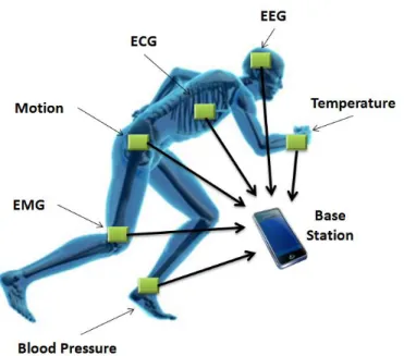
Biosensors are applied in trivial equipments and several gadgets, due to all technological and devices development many motes were created, performing monitoring physiological parameters [5]. Most of them measure health parameters like temperature, blood pressure, EMG (Electromyography), ECG (Electrocardiography), EEG (Electroencephalography) [12] as shown in Figure 2. This chapter will present some of the recent motes and applications developed, mostly focusing on monitoring and analyzing human body temperature motes.
Figure 2. Several Body Sensors Networks Applications.
Shimmer (Sensing Health with Intelligence, Modularity, Mobility and Experimental Reusability) [13] is a powerful sensor platform as shown in Figure 3. It uses a TinyOS [14] operating system. Some of the great features of this platform are the following: Wireless communication (Bluetooth and IEEE 802.15.4), microSD (micro Secure Digital) card slot allowing up to 2 Gigabytes of data, embedded 3-axis accelerometer and a Texas Instruments (TI) MSP430 microcontroller [15]. It uses a 250
Intra Body Sensors and Networks
8
mAh rechargeable battery for power supply. This sensor fits on a Printed Circuit Board (PCB) with 44mmx20mmx21mm. In [16], this mote was used to collect intra-vaginal temperature. This platform has a lot of potential for health applications due to communication technologies and technical features.
Figure 3. Shimmer mote.
Eco [17] mote is a miniaturized sensor mote with a dimension of 13mm x 10mm x 8mm as shown in Figure 4. It uses an nRF24E1 module that is a Radio Frequency (RF) transceiver with an embedded 8051 microcontroller. It has a 3-axial acceleration sensor, a temperature sensor and a light sensor. For powering, this sensor uses a 30mAh rechargeable battery. Due to the small size of this sensor mode, it has limitations when collecting long-term data. No extra memory support (like microSD slot) is available in this sensor; so long applications cannot be supported. In [18], this mote was used to detect spontaneous motion monitoring of preterm infants and in [17] for an interactive art performance. In the detection of spontaneous motion in preterm infants this application could help them as an support for their growth in weight and bone strength.
For the interactive art performance they put the node sensors in a dancer, which will transmit data motion, body temperature, heartbeat, and even surroundings ima ges. This mote allows the collection of a wide of sensing parameters from multiple types of sensing devices.
Intra Body Sensors and Networks
9
Figure 4. Eco Mote.
Figure 5 presents Tyndall [19] sensor which is a multiple layer sensor. Each layer is used as a module, and the sensor mote could be constructed only with the needed modules. Each module measures 25mm x 25mm and has different features like, wireless communication and various sensor types. The platform has a high-density connector which facilitates a data bus for configuration and data transfer between layers. Other layers like integration signal conditioning layer and sensor layers temperature allows interfacing to seven external sensors and functions as a temperature alarm.
Figure 5. Tyndall module.
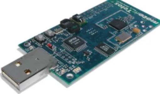
TelosB mote [20] is an experimental platform for lab studies as present in Figure 6. It provides several features such as USB and IEEE 802.15.4 communications, an MSP430 microcontroller and light, temperature and humidity sensors. It fits in 65mm x 31mm x 6mm and uses 2xAA batteries for power supply.
Intra Body Sensors and Networks
10
Figure 6. Telos module.
Figure 7 presents MICAz [21] mote which is a tiny wireless measurement system mote from Crossbow. It provides 2.4 GHz IEEE802.15.4 compliant RF transceiver designed specifically for deeply embedded sensor networks with low-power consumption. This mote uses an ATmega128L which is a low-power microcontroller and has an 51-pin expansion connector that supports additional analog inputs, digital I/O, I2C, SPI and UART interfaces. All theses interfaces make it easy to connect a wide variety of external sensor boards like expansion connector for light, temperature, RH, barometric, acceleration/seismic, acoustic, magnetic and others. Similar to TelosB this mote uses 2xAA batteries to be powered.
Intra Body Sensors and Networks
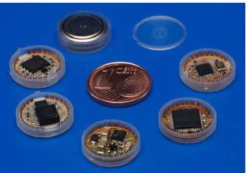
11 Small Autonomous Network Device (SAND) [22] is a modular application development platform for small wireless sensor or actuators. This platform is like any typical design of a mote with a small PCB and an embed microcontroller, many interfaces and a wireless communication block (IEEE802.15.4). This platform has the possibility of adding new blocks measuring 14mm of diameter and a volume of 1.5 cm3 each one and with a different functionality.
As shown in Figure 8, due to all its features and size this mote is well used for healthcare patients monitoring systems. SAND motes are easily assembled and C-programmable small sized enables fast and reduced cost field testing. As a result of its cylindrical shape a CR1225 coin cell battery is used to provide power on system.
Figure 8. SAND module.
DuoFertility [23] project created a system to predict women‟s fertile period by measuring and controlling the skin‟s temperature as present in Figure 9. This system comprises two modules, a wireless sensor mote placed under the arm of the monitored women and a remote reader unit. The sensor mote, used all the time, collects measurements of skin temperature and by demand the reader unit could retrieve these measures. This unit indicates with a light scale the probability of the fertile period occurring.
In [24] it‟s possible to see that the skin temperature varies with the environment where it is taken. So getting core body temperature leads to more reliable results.
Intra Body Sensors and Networks
12
Chapter 3
3.
System Requirements and
Architecture
This chapter elaborates on the description and the followed procedures to design the prototype. First, the problems and requirements for this project are presented. After, the chosen hardware for the prototype construction is described in detail.
3.1. Requirements
This section studies the system requirements that lead to this proposal of the sensor architecture in terms of its anatomic shape and size to be placed inside a vagina. The interaction with the sensor should be wireless and the sensor should have the ability to operate in a stand-alone mode.
Due to the working place of the proposed sensor, it has to respect some anatomic limitations, namely, it should be easy to be placed inside the vagina and comfortable because the main focus is helping prevent problems not cause them. Following a medical recommendation the sensor board and other peripheral parts has to fit in a container with about 60mm x 18mm of area. Therefore a size of 30mm x 16mm was the target for the main board with a microcontroller, a micro SD card slot, a transceiver (IEEE 802.15.4), and a computer interface included. The use of a shape similar to a trivial tampon seems to
System Requirements and Architecture
14
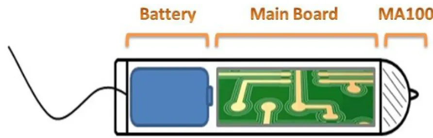
be a perfect choice. It is well known by women, easy to use, anatomically perfect, and it has the size to accommodate all the above-mentioned features. The tampon like the shape presented in Figure 10 has a conceptual design of the new proposed sensor. As may be seen, the thermistor is placed on the top of the container, the electronic circuit in the body of the container, and the battery on the tail. The enclosure to fulfill all the health conditions needs to be properly closed and avoid any way of contact with the exterior part. As known, the vagina is a humid place and no fluid should make contact with the electronic part to avoid electric conductivity. The electric current range used to power this circuit is not too high but enough to cause some health damages in sensitive and tender skin like burns or others injuries.
Figure 10. Conceptual design of the new intra-vaginal temperature monitoring sensor mote.
With woman‟s comfort in mind, the sensor should be operated when placed inside vagina. This feature avoids the need to take it out every time it is necessary to perform an operation to pick up the collection of measured temperature values. This feature will belong to this new sensor platform with the inclusion of a wireless communication module supporting the standard IEEE 802.15.4. This feature also allows re-configurations to the sensor operation mode without a physical connection to the programming dock/station.
Like many other nodes, a small rechargeable battery is considered. This battery supports a long lifetime, also due to the low-power system consumption. The power consumption is the main feature for any wireless sensor node in a way to achieve long-term operation. In WSN‟s it is expected that all nodes have a transceiver layer and a
System Requirements and Architecture
15 battery to get mobility, and spend most of the time in low-power state, waking up only when readings and transmissions are required [11] to achieve an application like in Figure 11.
Figure 11. System architecture.
The sensor is designed for collecting intra-body temperature measures for long periods of time (e.g. during a menstrual cycle). Thus, this feature will be guaranteed with the inclusion of a microSD slot for a large amount of data collection. The power supply must also provide long periods of operation time. The sensor design includes a rechargeable with regular voltage of 3.6V and capacity of 450mAh, which can easily cover the required power of all components for long periods of operation time.
For temperature measurements a thermistor was included. This thermistor will be used to measure the intra-vaginal temperature.
3.2. Hardware Description
This section gives a detailed description and features of the hardware components chosen to develop a single sensor board. The components will be described for its major functionality on the system, such as, Texas Instruments™ MSP430F2274 [25], Chipcon CC2420 [26], Antenova IMPEXA 2.4GHz Antenna [27], TPS60100 [28] and temperature sensor unit.
System Requirements and Architecture
16
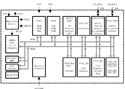
The Texas Instruments™ MSP430F2*** [25] is one of the core components of my baseboard and its primary advantages are its extremely low power during periods of inactivity and its proven history for medical sensing applications. The MSP430 is based upon the 16-Bit RISC CPU, peripherals and an adaptable clocking mechanism connected via a Von-Neumann memory address bus (MAB) and memory data bus (MDB). The architecture, combined with five low-power modes is optimized to achieve extended battery life in portable measurement applications. The device features a powerful 16-bit RISC CPU, 16-bit registers, and constant generators that contribute to maximum code efficiency. The digitally controlled oscillator (DCO) allows wake-up from low-power modes to active mode in less than 1μs. The Figure 12 illustrates an architectural overview of the CPU which shall be discussed under the following topics, Clocking, Memory, Timers, USART and ADC.
System Requirements and Architecture
17 The MSP430 clocking mechanism is designed to support a battery supply with low power consumption by allowing the user to select from three inherent clock signals to gain optimum correlation between performance selection and power usage. The three clocks are:
Auxiliary Clock (ACLK) which is a low frequency clock supplied by a 32KHz crystal, utilized for self wake-up and self-timing operation and low-power mode. Master Clock (MCLK), a high-speed clock which is fed from an internal digitally
controlled oscillator (DCO), selected using interrupt requests. This is used for high-speed signal CPU and peripheral applications. The DCO, which may operate up to 8MHz, can be activated from sleep mode in 6Is and allows the CPU to be operated in very quick bursts.
Sub-Main Clock (SMCLK) which is designed to utilize the DCO or standard crystal oscillators as necessary for peripheral operation.
The MSP430 contains 1K bytes of RAM, 32K bytes of flash and 256 bytes of information storage. The programming of the flash memory can be completed in system using the CPU or via the bootstrap loader or JTAG port. The flash memory can be used for storing both the data and the code and the CPU has the ability to write on the flash memory via single-bytes and single-words.
This microprocessor is equipped with two timers, Timer_A and Timer_B. Timer_A is a 16-bit asynchronous timer/counter which contains three capture/compare registers which allow for PWM outputs, interval timing and multiple capture/comparing. Timer_A also includes asynchronous input and output latching and the ability to generate interrupts depending on overflow conditions of the counter and capture/compare registers. Timer_B is identical to Timer_A with the additional functionality of having a programmable length (8, 10, 12, or 16 bits), double-buffered and group-able registers and the ability to force the outputs into a high-impedance state.
The MSP430 contains a USCI module used for serial data communication. The USCI module supports synchronous communication protocols like SPI (3 or 4 pin), I2C and
System Requirements and Architecture
18
asynchronous communication protocols such as UART, enhanced UART with automatic baud rate detection (LIN), and IrDA. USCI_A0 provides support for SPI (3 or 4 pin), UART, enhanced UART, and IrDA. USCI_B0 provides support for SPI (3 or 4 pin) and I2C. The hardware-universal asynchronous/synchronous receive/transmit serial communication USCI (USCI_A and USCI_B), as illustrated in Figure 12, which enable SPI (three-wire) and asynchronous UART functionality. The USCI_B allows I2C transmissions and has two specific DMA channels to ensure maximum throughput with data rates up to 400Kbps. The signal transmission and reception is possible using double-buffered channels.
The flow of the data transfer is possible using three or four pins; the slave in, master out (UCxSIMO), slave out, master in (UCxSOMI), USART SPI clock (UCxCLK) and slave transmit enable (UCxSTE) formats. In addition to master and slave modes 7 -bit or 8-bit addressing are also supported. For low power operation receiver start edge detection is incorporated for auto-wake up.
It has ADC10 module which supports fast, 10-bit analog-to-digital conversions. The module implements a 10-bit SAR core, sample select control, reference generator, and data transfer controller (DTC). The DTC allows ADC10 samples to be converted and stored anywhere in memory without CPU intervention. The module can be configured with user software to support a variety of applications. The ADC internal ports are being used to read data from the Temperature sensor. The maximum conversion rate of the ADC is greater than 200Kbps and the sampling period can be controlled by software or one of the internal timers. In my baseboard the MSP430 ADC core is only enabled when data acquisitions are needed.
The CHIPCON CC2420 [26] is a single-chip 2.4 GHz IEEE 802.15.4 compliant RF transceiver designed for low-power and low-voltage wireless applications [29-30]. The CC2420 includes a digital direct sequence spread spectrum base band modem providing a spreading gain of 9 dB and an effective data rate of 250 kbps. The CC2420 is a low-cost, highly integrated solution for robust wireless communication in the 2.4 GHz unlicensed ISM band. The RF transceiver also provides extensive hardware support for packet handling, data buffering, burst transmissions, data encryption, data authentication, clear
System Requirements and Architecture
19 channel assessment, link quality indication and packet timing information. These features reduce the load on the host controller and allow the CC2420 to interface with low-cost microcontrollers. The configuration interface and transmit / receive FIFOs of the CC2420 are accessed via an SPI interface. In a typical application the CC2420 will be used together with a microcontroller and the necessary passive and active components.
Figure 13. CC2420 functional blocks diagram.
Figure 13 illustrates a simplified block diagram of the CC2420, which features a low-IF receiver. The received RF signal is amplified by a low-noise amplifier (LNA) and down-converted in quadrature (I and Q) to the intermediate frequency (IF). At IF (2 MHz), the complex I/Q signal is filtered and amplified, and then digitized by the ADCs. Automatic gain control, final channel filtering, de-spreading, symbol correlation and byte synchronization are performed digitally. The SFD pin goes high when a start of frame delimiter has been detected. The CC2420 buffers the received data in a 128 byte receive FIFO. The user may read the FIFO through an SPI interface. Cyclic Redundancy Check
System Requirements and Architecture
20
bytes are verified in the hardware. RSSI and correlation values are appended to the frame. CCA is available on a pin in receive mode. Serial (unbuffered) data modes are also available for test purposes.
The CC2420 transmitter is based on direct up-conversion. The data is buffered in a 128 byte transmit FIFO (separate from the receive FIFO). The preamble and start of frame delimiter are generated by hardware. Each symbol (4 bits) is spread using the IEEE 802.15.4 spreading sequence to 32 chips and output to the digital-to-analog converters (DACs). An analog low-pass filter passes the signal to the quadrature (I and Q) up-conversion mixers. The RF signal is amplified in the power amplifier (PA) and fed to the antenna.
To complete the IEEE802.15.4 compliant wireless communication the Impexa 2.4GHz SMD Antenna from ANTENOVA was the better choice. This antenna is intended for use with all kinds of 2.4GHz applications such as in mobile phones, PDA‟s, PND‟s, headsets, MP3‟s, Laptops, PC-cards and Sensors. The antenna uses a ground plane in order to radiate efficiently, but this ground plane must not extend underneath the antenna itself. It is easy to integrate and is intended for SMD mounting. The antenna is available in two versions with the feed locations on the right or left of the antenna. Designed with small dimensions 6.1x3.9x1.1[mm] and very light weighing only with 0.05g. Table 1 presents all the performance features for the model used.
Table 1. Antenova Impexa 2.4ghz features. Typical
performance Conditions
Peak Gain 1.0 bBi
All data measured on both (right/left) Antenova‟s boards.
Data given for the 2.4-2.5 GHz frequency range
Average Gain -1.9 dBi
Average efficiency 65%
Maximum Return Loss -10 dBi
Maximum VSWR 1.9:1
The voltage regulator chosen was the Texas Instruments TPS60100 [28]. The TPS60100 charge pump provides a regulated 3.3V output from a 1.8V to 3.6V input. It
System Requirements and Architecture
21 delivers a maximum load current of 200 mA. Designed specifically for space critical battery powered applications, the complete charge pump circuit requires only four external capacitors. The circuit can be optimized for highest efficiency at light loads or lowest output noise. The TPS60100 consists of an oscillator, a 1.22V bandgap reference, an internal resistive feedback circuit, an error amplifier, high current MOSFET switches, a shutdown/start-up circuit, and a control circuit as shown in Figure 14.
Figure 14. TPS60100 functional blocks diagram.
Figure 15 illustrates MA100 [31] which is a NTC type thermistor from General Electric used and approved for medical applications. Thermistor is an excellent sensor with high sensibility for fast temperature changes.
System Requirements and Architecture
22
Figure 15. MA100 physical structure.
The thermistor electrical resistance can have a proportional (PTC type) or inversely (NTC type) variation with the increase of temperature. With MA100 this variation is negative because it is an NTC type (Negative temperature coefficient) so the resistance decreases with the increasing temperature as observed on Figure 16. The NTC type of thermistor is more sensitive than other resistive sensors like, RTD (Resistance Temperature Detectors) or Thermocouple. However being more sensitive means that it has a non-linear behavior so a circuit is needed to adjust the exponential curve in way that makes it proximally linear. Thermistors have a time constant which affects the time taken to make up 63% of the next temperature value. This time constant directly depends of the ground and the thermal couple of the sample. In power consumption the thermistor needs around 100mA of current to start and power dissipation around 2 mW/ºC. NTC Thermistors can have a stable acquisition in a range of -50ºC up to 150ºC.
System Requirements and Architecture
23 The battery chosen is a Lithium battery from GMBPower [32] as shown on Figure 17 measuring 15,5mmx13.5mm, with a capacity of 450mAh. This battery was chosen particularly due its circular shape and large capacity. As a regular battery, the nominal voltage will decrease as the battery is discharged. In order to provide a regular voltage of 3.3V on the system, a voltage regulator is needed.
Figure 17. 450 mAh battery.
3.3. Testbed Architecture
The architecture design proposed in this work follows the above-mentioned requirements and the proposed node includes the technical features to address these requirements. This sensor node requires a small size and needs a long lifetime in order to satisfy a large number of applications [2]. The sensor node includes a small PCB with a microcontroller, a small rechargeable battery, an external memory card slot header, and a low power radio chip. Figure 18 presents the blocks diagram of the architecture used in the construction of the proposed sensor testbed.
System Requirements and Architecture
24
Figure 18. Biosensor block diagram of the proposal.
Following, is a detailed description of identified and selected components to create the sensor. It includes the following elements: microcontroller (CPU), power source, data storage, communication device, and the sensor to collect temperature values. The microcontroller is the main element of the sensor because it influences the rest of the solution; a microcontroller with low cost and low dynamic power consumption is essential. Thus, the Texas Instruments MSP430F1611 [15] was the choice for our testbed because it is an equipment that I have already used before and it fulfills the most needed requirements for the testbed implementation. Besides the intention to develop a miniaturized sensor prototype I will describe in detail the selected microcontroller, the MSP430F2274. Both microcontrollers are similar but the latter has small pin configuration (38 pins), with an optimal package style and doesn´t need a thermal pad, which will ensure the possibility of miniaturization. The MSP430F2274 microcontroller has fast start-up times, being very important in low duty cycle embedded applications. For these reasons, the selection of the MSP430F2274 is appropriated taking into account the following characteristics: 1Kbyte RAM, 32Kbyte Flash, supports up to 16MHz, and
System Requirements and Architecture
25 offers 1.8-3.6V operation which guarantee good expectations for all sensor development. Furthermore, this micro was chosen because of its relatively low pin count (38 pins). In this specific software design, the MSP430 operates in two modes: ACTIVE Mode (270 µA at 1 MHz) and OFF Mode (RAM retention at 0.1 µA). The highest features presented allowing the possibility of the integration of new future sensors for other applications.
For communication purposes, the Chipcon CC2420 [26] is a true single-chip with 2.4GHz IEEE 802.15.4 compliant RF transceiver, perfect for low power and low voltage wireless applications. This chip has a digital direct sequence spread spectrum baseband modem providing a gain of 9dB and an effective data rate of 250 kbps. The antenna adopted seems to be a good option because it is intended for 2.4GHz applications using Zigbee® [8]. This antenna is easy to integrate, has a high efficiency, and is light weight. In order to obtain high efficiency, the antenna was designed for use with no ground beneath the antenna but this ground plane must not extend underneath the antenna itself. The size of the antenna is 6.1mm x 3.9mm x 1.1mm, and with a weight of 0.05g.
For a sensor node, in many applications and usage, it is highly relevant to have big data storage. Then, the memory size is a limitation because the microcontroller only has 1kbyte RAM and 32Kbyte Flash, which is not enough to record continuous data during a week. The major advantage of the sensor is providing an external microSD card with up to 2Gbytes of memory. This feature adds a way to use applications where the storage amount of data is a real problem, mainly, in most cases where the small size of the motes is a key issue.
In this proposed testbed, as shown in Figure 19, a power supply is used to power the testbed but, for a final prototype, Lithium batteries already tested will be used. The chosen battery is a Lithium battery from GMBPower [32], model ER13150 measuring 15,5mm x 13,5mm, with a capacity of 450mAh. This battery was chosen particularly due its circular shape and large capacity, with full features for my application.
System Requirements and Architecture
26
Figure 19. Physical testbed for temperature monitoring.
For the design of the temperature sensor, the MA100 [31] thermistor was chosen. It is an NTC Type MA Biomedical Chip thermistor developed by GE Industrial Sensing and exclusively used for biomedical applications. Its main features fulfill the requirements of our solution. Its sensitivity ranges from 0ºC to 50ºC, with size of 0.762 x 9.52 mm. The size, shape, temperature ranges, and its approval for medical applications were the major reasons for this choice. To get more accurate temperature readings and taking into account its goal, the temperature sensor must be placed inside the female cervix, which is an ideal thermal source to reach the core body temperature. For this proposed architecture, the MA100 is embedded in the mote platform.
Using Zigbee [8] communication, temperature monitoring can be performed in a real-time mode. Also, the sensor platform saves measured values in the embedded microSD card and it also sends them to external devices in Zigbee range area. This wireless communication is also used to transfer all the data stored in the sensor‟s microSD card on demand.
Another important feature of this solution is mobility. After mote activation and correct placement inside vagina, the woman can move freely and do whatever she wants with comfort. After switching on the data collection (operation performed through remote
System Requirements and Architecture
27 commands), the sensor starts measuring and continuously storing data in the microSD card. The monitored woman only has to take the sensor out when the date advised by the doctor has been achieved. During a long monitoring period, the sensor need only be removed for battery recharge.
For a regular medical observation, a doctor can use the mote to measure current core temperature of a patient in his office with a real-time connection to the sensor, as above described. On the other hand, he can connect to the sensor directly and retrieve all collected data to his computer. In both cases the doctor can monitor and control the evolution of this biological parameter observing a graphical representation of the measured values.
Chapter 4
4.
Intra-Vaginal Temperature
Biosensor
This chapter introduces the project design of the intra-vaginal temperature biosensor. The biosensor schematics, the created electronic components, temperature conversion and the final layout for the main board will be described in detail. Finally, it will be presented how the temperature sensor was integrated in the main PCB board and how the firmware is structured.
4.1. Biosensor Project Design
The conception of this biosensor could only be possible because of the use of Altium Designer which is a software tool for schematic design. It can be used to design analog circuits, revise digital schematic diagram for an existing PCB or complete a hierarchical block design. Apart from designing, it also provides various built-in features for design verification and manufacturing processing. Altium Designer capture provides a component information system that allows one to identify, utilize and design with preferred parts. In the following subsection, a detailed description of the features provided by Altium capture and Altium layout are discussed.
Intra-Vaginal Temperature Biosensor
30
The main features of Altium Designer are the following:
1. The entire product development process with a single unified design solution
The designer could achieve a single solution to develop hardware, programmable hardware and software; it could take designs from concept to manufacture within a single unified environment and also, a single model of the design data, and a single design data storage system.
2. Freely explore design concepts „on-the-fly‟
Have the possibility to explore devices from different vendors with minimal design reengineering and easily explore design concepts and options before committing to final hardware. It makes things easy to use IP from any source, without being restricted to vendor-specific „sticky IP‟.
3. Rapidly prototype using a live, interactive hardware development system
The ability to develop, explore and debug designs on real hardware, in real-time with „LiveDesign' is easily achieved and harness the full potential of reprogrammable devices with soft-centric design. It is very quick on changing software and hardware with equal ease and on-the-fly.
4. Smooth the path from design to board layout and manufacture
The single centralized data source simplifies version control and component management and allows visualizing and interacting with board designs in real-time 3D, within the PCB editor. Everything it‟s possible with the seamless collaboration with MCAD designers and other engineering teams.
Intra-Vaginal Temperature Biosensor
31 5. Easily connect to wider company systems
Single access point for all design data simplifies links for data management systems and easily plug-in capability and built-in interfaces for external data management. It also has all involved in product development process access one design environment.
6. Be equipped for the future with the latest design technologies
It allows you to expand existing skill sets while harnessing the latest devices and techniques and make soft design and the creation of device intelligence the focus of design. Have the possibility to immediately access new technology through consistent and frequent updates.
7. Be productive right „out-of-the-box‟
For all tools and technologies in the box, including parts libraries and royalty-fee IP and no need to purchase costly add-ons to make a complete solution. It could continually updated with latest devices and technologies.
A project in Altium Designer consists of links to all documents and setups related to a design. A project file, eg. xxx.PrjPCB, is an ASCII text file that lists which documents are in the project and related output setups, eg. for printing and CAM. Documents that are not associated with a project are called 'free documents'. Links to schematic sheets and a target output, e.g. PCB, FPGA, embedded (VHDL) or library package, are added to a project. Once the project is compiled, design verification, synchronization and comparison can take place. Any changes to the original schematics or PCB, for exa mple, are updated in the project when compiled.
Intra-Vaginal Temperature Biosensor
32
The process of creating a new project is the same for all project types. For the creation of the sensor board, it will be used the PCB project type. On the PCB project it will be added all the schematic sheets needed to create the connections between the component parts. A schematic folder is simply a collection of schematic pages that are logically connected by off-page connector or hierarchical ports and pins. Off-pages connectors or separate schematic pages within a schematic folder are electrically connected if they have the same name. Similarly, wire segments (Netlabel) and off-page connectors on the same schematic page are electrically connected if they have the same name.
Figure 20. Altium schematic editor workspace.
The Altium Workspace shown in Figure 20 has shortcuts which make it easy to place the parts for my design. After placing the parts and electrically connecting them all
Intra-Vaginal Temperature Biosensor
33 the electrical information is stored in the design, making it easy to progress from placing parts to creating a netlist. When you place a part on a schematic page, the part can be placed without a reference designator assigned to it or it can have one automatically assigned. The Altium Designer has a lot of parts and components libraries from all the main electronic manufactures and some libraries must be added to support the schematics. Due to the variety of components and case styles, for some components have to be created. After all these parts are done, it will be created a blank PCB and add it to the project as well.
4.1.1. Making new Libraries and Parts
With Altium is not necessary to keep track of multiple libraries for each part. All the information presented on the Schematic library folder about every part in the design is kept in the design itself. Designs in Altium are self-contained and portable. The SCH Library displays all the parts in the library if you open and expand it. A library can contain parts, packages, symbols and schematic folders. In a library, they are all treated as parts. It is possible to move parts from one library to another by just dragging and dropping it. You can also copy a schematic folder to a library. Most of the parts used in the evaluation board were unavailable in the Altium Libraries. Therefore, the custom parts for some of the chips have to be build. To store all of these parts a new library was created. It is very straightforward to create libraries in Altium. In the Project menu, select “Add New to Project” and “Schematic Library” and a new library gets added to the design. The parts mentioned above were added to this library. To create new parts in Altium:
Select on the Schematic Library Documents the file with the extension .SchLib and on the SCH Library sheet selected on the bottom of the Altium environment click “Add”.
Intra-Vaginal Temperature Biosensor
34
In the components box assign a new component name, doing that a new schematic component will appear and after click in “Edit” more characteristics could be added.
An empty part outline appears in the part editor. To draw the part, uses the toolbar buttons on the top of the screen.
To add pins click “Add” on the Pins box.
Specify the pin name and number, and whether the pin represents one signal or a bus.
Pin shape and type determine the pin´s appearance and electrical characteristics. When placed one pin, Altium automatically increments the pin numbers.
After placing all the pins, the type of footprint can finally be added by clicking “Add Footprint”.
Using the steps above, new parts MSP430F2274, CC2420, TPS60100, 16MHz Crystal and Impexa Right Antenna were designed and are shown in Figure 21.
Intra-Vaginal Temperature Biosensor
35
4.1.2. Biosensor Board
Apendix A shows the main sheet of the schematic design of the Sensor board. A schematic folder is simply a collection of schematic pages that are logically connected by off-page connectors (Netlabel) or hierarchical ports and pins. It illustrates the Netlabel interface between the MSP430 microcontroller, CHIPCON CC2420, micro SD slot lines, JTAG lines, battery lines, antenna, linear voltage regulator and all the parts for signal acquisition. As shown all the parts are mostly connected using Netlabel which are wire shortcuts, substitutes for wire connections. It also shows the connections between CHIPCON CC2420 and the Impexa 2.4GHz SMD Antenna from ANTENOVA. The micro SD slot integration with the microcontroller is shown to allow backup storage of data and will be ready to integrate the socket if needed.
The main board has a JTAG interface lines that give access to the chip for debugging and can be used to download firmware to the MSP430.
Intra-Vaginal Temperature Biosensor
36
According to Figure 22, it is possible to see how the components were arranged on the board. On the top layer are all the main components and the bottom layer were only used to put some secondary electronic parts because some components like CC2420 and TPS60100 have a thermal pad. Below a thermal pad any parts can be placed, or below the antenna field in a way that achieves an optimal strength of wireless signal. For a better consistency with the parts connections, Table 2 shows all the connections port pins and what label is used to connect the different parts.
The main board uses the USCI interface, it can support multiple serial communication modes with one hardware module. In my design I only use the synchronous peripheral interface or SPI. The USCI can provide USCI_Ax and USCI_Bx modules that can be used for SPI mode. The USCI_B was used to do the interface between the CC2420 and the USCI_A between the micro SD lines.
Table 2. Port pins and signal names
MSP430F2274 Pin Signal Name External connection to
P3.2/UCB 0SOMI/UCB 0SCL UCBoSOMI
CC2420
P3.1/UCB 0SIMO/UCB 0SDA UCBoSIMO P3.3/UCB 0CLK /UCA 0STE UCBoCLK
P2.0/ACLK /A0/OA0I0 P2.0 P2.2/TA 0/A2/OA0I1 P2.2 P2.5/Rosc P2.5 XIN /P2.6 P2.6 P4.0/TB0 P4.0 P4.1/TB1 P4.1 P4.2/TB2 P4.2
P3.0/UCB 0STE /UCA 0CLK /A5 UCAoCLK
mSD lines
P3.5/UCA 0RXD /UCA0SOMI UCAoSOMI P3.4/UCA 0TXD /UCA0SIMO UCAoSIMO
Intra-Vaginal Temperature Biosensor
37
4.2. Temperature Sensor Integration
The integration of the temperature sensor into the small biosensor board was definitely the biggest challenge for this work not excluding the board design. As known the MA100 thermistor was the chosen temperature sensor, and according to this type of sensor (NTC) some additional electrical equipment needs to be joined to ensure a linear behaves from the resistance. For NTC thermistor type a Wheatstone bridge and an operational amplifier is normally used to ensure a linear behavior from the thermistor. Due to the features of the microcontroller used in this design it‟s not necessary to add differential amplifiers because the micro already has two configurable operational amplifiers. As shown in Figure 23, the Wheatstone bridge was created to measure resistors, in this specific case the thermistor resistance and the differential amplifiers don´t need to be added because they are already internally on the microcontroller by correct configuration.
P4.3/TB0/A12/OA0O P4.3 P1.7/TA 2/TDO /TDI TDO
pJTAG lines
P1.6/TA 1/TDI TDI
P1.5/TA 0/TMS TMS
P1.4/SMCLK/TCK TCK
RST /NMI /SBWTDIO RST TEST/SBWTCK TEST/SBWTCK
Intra-Vaginal Temperature Biosensor
38
Figure 23. Thermistor signal acquisition circuit.
(1)
Equation (1) presents the relation between the two points on the Wheatstone
bridge, this will generate the value of the differential tension on those two poi nts (OAo_IN and OA1_IN). This value will be calculated internally by the microcontroller and will be converted to digital on the ADC10 lines available considering the gain of the circuit amplifier detailed described on Table 3. According to the proposed circuit some internal configurations need to be made to select the correct amplifier settings. As referred the microcontroller operational amplifiers can be configured with the OAFCx bits and to obtain a differential amplifier function it needs to acquire “111” value. This mode allows internal routing of the OA signals for a two-opamp or three-opamp instrumentation amplifier. I will use a two-opamp configuration with OA0 and OA1. In this mode the buffer is combined with one or two remaining OAx to form the differential
Intra-Vaginal Temperature Biosensor
39 amplifier. For two-opamp differential configuration amplifier the control register settings will combine this form OA0CTL0 = xx xx xx 00; OA0CTL1 = 000 111 0x; OA1CTL0 = 11 xx xx x x; OA1CTL1 = xxx 110 0x and the OA1 OAFBRx register for Gain setting will assume “101” to obtain a “4 1/3” value.
Table 3. Analogic to digital adc10 conversion values.
T (ºC) RTH (kΩ) VADC (V) Converted value (V) Converted value
25 10 0,5882 2,5490 1044 26 9,57232 0,5667 2,4559 1006 27 9,16529 0,5450 2,3615 967 28 8,77779 0,5229 2,2659 928 29 8,40868 0,5005 2,1690 888 30 8,05731 0,4780 2,0711 848 31 7,72243 0,4551 1,9722 808 32 7,40329 0,4321 1,8723 767 33 7,09842 0,4088 1,7713 726 34 6,80836 0,3853 1,6697 684 35 6,53131 0,3617 1,5672 642 36 6,26575 0,3378 1,4636 599 37 6,01647 0,3141 1,3611 558 38 5,77605 0,2901 1,2571 515 39 5,54653 0,2660 1,1528 472 40 5,32734 0,2419 1,0481 429 41 5,11797 0,2176 0,9431 386 42 4,91794 0,1934 0,8381 343 43 4,72677 0,1691 0,7330 300 44 4,54391 0,1449 0,6278 257 45 4,36933 0,1207 0,5229 214 46 4,20084 0,0963 0,4172 171 47 4,04081 0,0721 0,3125 128 48 3,88951 0,0483 0,2094 86 49 3,74317 0,0244 0,1056 43 50 3,60310 0,0005 0,0023 1
Intra-Vaginal Temperature Biosensor
40
4.3. Firmware Development
The communication between Biosensor and computer is performed by a Wi-Fi connection. The computer sends operating commands to Biosensor, which in turn, sends information and data to computer. Biosensor always waits for computer commands over the Wi-Fi connection. Once a command is received then it proceeds accordingly. The operating commands available in the Biosensor are the following:
Start: when Biosensor receives this command, it starts collecting temperature measurements in the MicroSD™ card. If a Wi-Fi connection continues available temperature measurements are also delivered to computer for real-time monitoring and analyses. If no connection is available, temperature measurements are only written in MicroSD™ card. That way, Biosensor prevents unnecessary use of Wi-Fi connection and allows increasing the battery lifetime.
Stop: this command stops the collection of new temperature measurements.
Get: this command performs the transmission of all temperature measurements gathered in MicroSD™ card to the computer application for further study and analysis.
Figure 24 presents the firmware diagram developed for the Biosensor. This firmware provides all the above-mentioned features.
Intra-Vaginal Temperature Biosensor
41
Figure 24. Biosensor firmware diagram.
The analysis of temperature measurements is performed in off-line mode. So to ensure good results, it is vitally important to know the exact time when each temperature measurement is taken. Biosensor only has a local time clock, which starts on Biosensor start up. This clock can‟t give the real global time clock. To associate each measurement with the right global time clock instant, when a start command is send to Biosensor, computer also sends its clock and date time (assuming computer clock is global clock synchronized). This information is then used by Biosensor firmware as an offset to local time clock in order to calculate the exact global time clock for every insta nt of temperature measurements.


![Figure 5 presents Tyndall [19] sensor which is a multiple layer sensor. Each layer is used as a module, and the sensor mote could be constructed only with the needed modules](https://thumb-eu.123doks.com/thumbv2/123dok_br/18842720.928901/37.918.347.571.115.287/figure-presents-tyndall-sensor-multiple-sensor-constructed-modules.webp)