Printing of eco‐friendly solution
based zinc‐tin oxide for device
applications
Supervisor: Doctor Rita Maria Mourão Salazar Branquinho, Invited Assistant
Professor, FCT‐UNL
Co‐Supervisor: Cristina Gaspar, Research Scientist, FCT‐UNL
Monitor: Emanuel Abreu Antunes Carlos, PhD Student, FCT‐UNL
Rita de Vasconcelos Pereira
Licensed in Materials EngineeringOctober 2019
Dissertation to obtain the master degree in Materials Engineering
Jury:
President: Dr. João Paulo Miranda Ribeiro Borges, Associate Professor with aggregation of Materials Science department, FCT-UNL
Arguer: Dr. Pedro Miguel Cândido Barquinha, Associate Professor of Materials Science department, FCT-UNL
Vowel: Dr. Rita Maria Mourão Salazar Branquinho, Invited Assistant Professor of Materials Science department, FCT-UNL
Printing of eco-friendly solution based zin-tin oxide for device applications
Printing of eco-friendly solution based zin-tin oxide for device applications
III
Printing of eco‐friendly solution based zinc‐tin oxide for device applications
Copyright © Rita de Vasconcelos Pereira, Faculdade de Ciências e Tecnologia, Universidade Nova
de Lisboa
A Faculdade de Ciências e Tecnologia e a Universidade Nova de Lisboa têm o direito, perpétuo e sem limites geográficos, de arquivar e publicar esta dissertação através de exemplares impressos reproduzidos em papel ou de forma digital, ou por qualquer outro meio conhecido ou que venha a ser inventado, e de a divulgar através de repositórios científicos e de admitir a sua cópia e distribuição com objetivos educacionais ou de investigação, não comerciais, desde que seja dado crédito ao autor e editor.
Printing of eco-friendly solution based zin-tin oxide for device applications
Printing of eco-friendly solution based zin-tin oxide for device applications
V
Acknowledgements
First of all I would like to thank to the Faculty of Science and Technology of the Universidade NOVA de Lisboa and to my department, Materials Science for welcoming me and allowing me to take the course over these extraordinary years. Thank you also to the coordinator of my course João Paulo Borges for his dedication and availability.
I would also like to thank to Professor Rodrigo Martins and to Professor Elvira Fortunato for allowing me to do this work in the facilities of CENIMAT||3N and CEMOP laboratories which offered me excellent conditions to investigate all I need to carry out this study.
To my co-supervisor Cristina Gaspar and to my supervisor Rita Branquinho, I am so grateful for her to trust me and accepting me as her student for this subject and who, despite having always a thousand things to do, she was always present and support me whenever I needed.
A huge thank you to Emanuel Carlos, my monitor during this thesis, for everything he taught me, for being always present during this 8 months, for scolding me when I needed it and for all the support he always provide me, giving me all the knowledge I needed to do this work. Thank you so much.
I would also like to thank the SuperSmart project where my thesis was integrated.
Thanks to João Ribas for the knowledge exchange and for the data he provide me, to Bernardo Rodrigues for teaching me how to handle the Inkjet machine and to all those, in some way, helped me during this months, Alexandra Gonçalves, Sónia Pereira, Ana Pimentel, Joana Neto, Tomás Calmeiro, Inês Cunha, Raquel Teixeira and Sara Silvestre.
To my colleagues, Carlos Dias, João Rolo and Hadassa for making the hours spent in the lab more fun. I would like to thank to my colleagues, partners and friends of the course, Joana, Adriana, Bia, Sara, David, Parada, Tomás, João Duarte and Oliveira for always being with me, for accompanying me throughout these years, for all the moments they have given me, they make my passage for this course easier and better. Thank you for everything.
Thank you to all my teammates of the AEFCT Futsal Feminino, for giving me unforgettable moments both inside and outside the court, you are machines! A special thanks to Aninhas and Patricinha for accompanying me from the beginning and for all that I learn from them.
To my goddaughters, Tânia, Marta, Su and Beatriz for always being by my side all these years and supporting me no matter what. Without them it would not have been the same.
To my godmothers, Carolina Pires and Carolina Reis for helping me whenever I need both academic and personal.
To my old friends, Mariana, Margarida, Filipa and Sami who over the years have never let me down, I know I can count on them for the rest of my life. Thank you.
To my family who was always present, parents, grandparents and uncles for all the support. Of course my brother and sister, Miguel and Catarina, my cousins, Alice and Diana and to Teresa.
To my boyfriend João, for being with me since the beginning, for all the support, for always believe in me and for make me happy, you make everything so much better.
Printing of eco-friendly solution based zin-tin oxide for device applications
Printing of eco-friendly solution based zin-tin oxide for device applications
VII
Abstract
The research of amorphous metal oxide semiconductors for printed electronics applications, such as transparent and flexible devices, has been increasing to allow the low-cost production, good performance and large area upscaling of these materials.
The most commonly used solution-based semiconductors rely on toxic solvents and are indium-based. To avoid this critical raw material ZTO is the preferred alternative. Nevertheless, replacing the toxic solvent and the chloride-based tin precursor wich also contributes to the toxicity of the solution remains a challenge.
This work focuses on the development of eco-friendly ZTO precursor solutions to produce electronic devices at low temperature and optimization of flexographic printing of these ZTO inks.
ZTO/SiO2 TFTs were successfully produced at 300 °C with non-toxic solvent, presenting a mobility of 2.98 ± 0.05 cm2/V.s and flexoprinted Ag/ZTO/ITO Schottky diodes were successfully produced at low temperature (150 °C + DUV) with a current on/off ratio of 1000. These devices show equivalent performance to the current state-of-the-art of ZTO devices produced with toxic solvents.
Finally, TFTs and Schottky diodes using non-toxic solvent and chloride-free ZTO precursors were successfully demonstrated for the first time.
This work clearly shows that it is possible to produce 100 % eco-friendly inks for high performance devices at low temperature suitable for large area printing.
Key-words: Amorphous metal oxide semiconductors, Printed electronics, Flexographic printing, Non-toxic solvent, TFTs, Schottky diodes, Low temperature
Printing of eco-friendly solution based zin-tin oxide for device applications
Printing of eco-friendly solution based zin-tin oxide for device applications
IX
Resumo
Os semicondutores de óxidos metálicos amorfos têm sido investigados em aplicações de eletrónica impressa, nomeadamente em dispositivos transparentes e flexíveis, permitindo a produção de baixo custo, bons desempenhos dos dispositivos e a produção em larga escala deste tipo de materiais.
Os semicondutores baseados em solução mais usados são normalmente compostos por índio e com solventes tóxicos. De forma a evitar estes materiais críticos ZTO é uma boa alternativa. A substituição destes solventes tóxicos e do precursor de estanho baseado em cloretos permanece um desafio.
Este trabalho foca-se no desenvolvimento de uma solução ecológica precursora de ZTO para a produção de dispositivos eletrónicos a baixa temperatura e a otimização da técnica de impressão de flexografia de tintas de ZTO.
TFTS de ZTO/SiO2 foram produzidos com sucesso a 300 °C com um solvente não-tóxico, apresentando uma
mobilidade de 2.98 ± 0.05 cm2/V.s e díodos de Schottky impressos por flexografia de Ag/ZTO/ITO foram também produzidos com sucesso a baixa temperatura (150 °C + DUV) com uma razão de corrente on/off de 1000. Estes dispositivos mostraram desempenhos equivalentes ao presente estado de arte de dispositivos de ZTO produzidos com um solvente tóxico.
Finalmente, TFTs e díodos de Schottky baseados em solução com solvente não-tóxico e com precursores de ZTO livres de cloretos foram demonstrados com sucesso pela primeira vez.
Este trabalho mostra claramente que é possível produzir tintas 100 % ecológicas para a produção de dispositivos com altos desempenhos a baixa temperatura ajustável para impressões à larga escala. Palavras-chave: Semicondutores de óxido de metal amorfo, Eletrónica impressa, Flexografia, Solvente não-tóxico, TFTs, Díodos de Schottky, Baixa temperatura
Printing of eco-friendly solution based zin-tin oxide for device applications
Printing of eco-friendly solution based zin-tin oxide for device applications
XI
List of Abreviations
2- ME- 2- Methoxyethanol AFM- Atomic Force Microscopy
AMOS- Amorphous metal oxide semiconductor ATR- Attenuated total reflectance
CEMOP- Center of Excellence in Microelectronics and Optoelectronics Processes CENIMAT – Centro de investigação de materiais
DSC- Differential scanning calorimetry DUV- Deep ultraviolet
FET- Field effect transistor
FTIR- Fourier transform infrared spectroscopy HP- Hot plate
IGZO- Indium-gallium-zinc oxide IPA- Isopropyl alcohol
ITO- Indium-tin oxide IZO- Indium-zinc oxide LCDs- Liquid crystal displays
MIS- Metal-Insulator-Semiconductor M-O-M- Metal oxide metal
MP- 1- Methoxy-2-Propanol NIR- Near-infrared
OLEDs- Organic light-emitting diodes PET- Polyethylene terephthalate PTFE- Polytetrafluorethylene PVD- Physical vapor deposition R2R- Roll-to-roll
rpm- Rotations per minute
SCS- Solution combustion synthesis TFTs- Thin film transistors
TG- Thermogravimetry UV- Ultraviolet VIS- Visible
XRD- X-ray diffration ZTO- Zinc-tin oxide
Printing of eco-friendly solution based zin-tin oxide for device applications
Printing of eco-friendly solution based zin-tin oxide for device applications
XIII
List of symbols
µ - Mobility (cm2/V∙s)
µFE - Field-effect mobility (cm2/V∙s)
µSAT – Saturation mobility (cm2/V∙s)
Ci - Gate capacity per unit area (F/cm2)
Eg- Bad gap energy (eV) ID- Drain current (A)
L – Channel Length (µm) SS- Subthreshold Slope (V/dec) VG- Gate Voltage (V)
VT - Threshold voltage (V)
Printing of eco-friendly solution based zin-tin oxide for device applications
Printing of eco-friendly solution based zin-tin oxide for device applications
XV
Table of Contents
1. Introduction ... 1
1.1. Amorphous metal oxide semiconductors ... 1
1.2. Toward lower process temperature... 1
1.3. Printing techniques: Flexography Printing and Inkjet Printing ... 2
1.4. Thin Film Transistors: TFTs ... 2
1.5. Schottky diodes ... 4
2. Materials and methods ... 7
2.1. Precursor Solutions Preparation and Characterization ... 7
2.2. Thin Film Deposition and Characterization ... 7
2.3. Electronic Device Fabrication and Characterization ... 8
3. Results and Discussion ... 9
3.1. Effect of ZTO ink proportion, precursor and concentration on stability and quality of the ink. ... 9
3.1.1. Stability of solutions ... 9
3.1.2. Aging of the solutions ... 10
3.1.3. Viscosity of solutions ... 10
3.1.4. Thermal characterization of solutions ... 11
3.2. ZTO thin films characterization... 11
3.2.1. Fourier Transform Infra- Red (FTIR) spectroscopy ... 11
3.2.2. Optical characterization... 12
3.2.3. Structural characterization ... 13
3.3. Electrical characterization of ZTO devices ... 14
3.3.1. TFTs ... 14
3.3.2. Schottky diodes ... 16
3.4. Flexographic Printing of ZTO thin films ... 19
3.4.1. Characterization of flexible substrates ... 19
3.4.2. Optimization of flexographic printing parameters ... 21
3.4.2.1. Printing pressure ... 21
3.4.2.2. Surface plasma treatment ... 22
3.4.2.3. Ink and substrate characteristics ... 22
3.4.3. Electrical characterization of printed diodes ... 24
4. Conclusion and Future perspectives ... 29
5. References ... 31
6. Annexes ... 33
Annex 1 ... 33
Annex 2 ... 33
Printing of eco-friendly solution based zin-tin oxide for device applications
XVI
Annex 4 ... 35 Annex 5 ... 37 Annex 6 ... 38
Printing of eco-friendly solution based zin-tin oxide for device applications
XVII
List of Figures
Figure 1.1- Flexography Printing Scheme [4]... 2
Figure 1.2- (a) 2D schematic of the straight section of a TFT [14] and (b) 3D scheme of a TFT [1] ... 3
Figure 1.3- Energy band diagram of an ideal TFT for different bias conditions [13] ... 3
Figure 1.4- Typical (a) output and (b) transfer curves of a n-type oxide TFT [13] ... 4
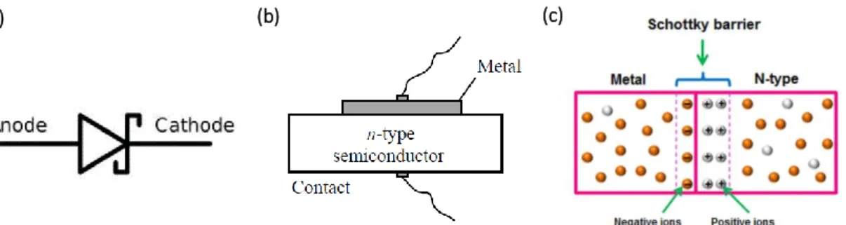
Figure 1.5- (a) Schottky diode symbol, (b) 2D scheme of a schottky diode and (c) Schottky barrier scheme [23] ... 5
Figure 1.6- The electron energy relations of a metal and an n-type semiconductor [23] ... 5
Figure 1.7- Variation of the voltage drop between the pn junction diode and a schottky diode ... 6
Figure 2.1- Scheme of the procedure to produce TFTs and Schottky diodes... 8
Figure 3.1- (a) Tin chloride solutions, (b) Zinc nitrate solution in MP and (c) tin acetate in MP solution ... 9
Figure 3.2- (a) Solution with combustion (1:1) and (b) Solution without combustion (2:1) ... 9
Figure 3.3- Variation of viscosity with the concentration of solution of ZTO inks prepared with and without urea ... 10
Figure 3.4- TG-DSC analysis of a ZTO precursor solution with combustion (1:1), with 0.2 M concentration ... 11
Figure 3.5- FTIR spectra for ZTO thin films produced from different precursor solutions. ... 12
Figure 3.6- Transmittance spectra of combustion ZTO (1:1) thin films ... 12
Figure 3.7- XRD spectrum of ZTO thin film ... 13
Figure 3.8- IV transfer curves of TFTs produced by ZTO precursor solution 0.1 M concentration (a) without combustion (2:1) (inset photograph of the TFTs produced) and (b) with combustion (1:1) on Si/SiO2 wafer. ... 14
Figure 3.9- IV Output curve of TFTs produced by ZTO precursor solution 0.1M concentration, on Si/SiO2 wafer. ... 14
Figure 3.10- IV transfer curves of TFTs produced by ZTO precursor solution without combustion (2:1), 0.1M concentration, on Si/SiO2 wafer, after 3 months ... 15
Figure 3.11- IV transfer curves of TFTs produced with Cl-free ZTO precursor solution without combustion (a) (1:1) and (b) (2:1), 0.05M concentration, on Si/SiO2 wafer. ... 16
Figure 3.12- IV curves of diodes produced by ZTO precursor solution with combustion (1:1), 0.6M concentration, on glass with ITO, with contacts deposited by thermal evaporation, (a) linear scale (inset photograph of the Schottky diodes produced) and (b) logarithmic scale ... 17
Figure 3.13- IV curves of diodes produced by ZTO precursor solution with combustion (1:1), 0.6M concentration, on glass with ITO, with contacts deposited by Inkjet. (a) Linear scale and (b) logarithmic scale. ... 17
Figure 3.14- IV curves of diodes produced by ZTO precursor solution with combustion (1:1), 0.6M concentration, on glass with ITO, with contacts deposited by Inkjet, 2 weeks later. (a) Linear scale and (b) logarithmic scale. ... 18
Figure 3.15- IV curves of Schottky diodes produced by ZTO precursor solution, where tin chloride was replaced by tin acetylacetonate, 0.6M concentration, on glass with ITO, contacts deposited by Ebeam. (a.1) and (a.2) with an annealing treatment at 250 °C in HP in linear and logarithmic scale respectively and (b.1) and (b.2) With an annealing treatment at 150 °C + DUV in linear and logarithmic scale respectively. ... 18
Figure 3.16- Variation of roughness on different used substrates on flexographic printing: Kapton 50µm, PET with ITO and Kapton 75µm ... 20
Figure 3.17- Resistances of substrates before and after annealing treatment of 30 minutes at 150 °C + DUV ... 21
Figure 3.18- Variation of Pressure between the mask and the substrate no prints ... 22
Figure 3.19- Effect of plasma treatment on prints. (a) Print without plasma treatment and (b) print with plasma treatment. (c) Kapton under the O2 plasma treatment ... 22
Figure 3.20- Prints on paper with Ag nanowires integrated. (a) ZTO precursor solution 0.6M with combustion (1:1) and (b) ZTO precursor solution 0.6M (1:1) where tin chloride was replace by tin acetylacetonate. ... 24
Printing of eco-friendly solution based zin-tin oxide for device applications
XVIII
Figure 3.21- Used mask to deposit the contacts by electron beam assisted thermal evaporation. ... 24
Figure 3.22- IV curves of diodes produced by ZTO precursor solution (a.1) and (a.2) 0.6 M in linear and logarithmic scale respectively and (b.1) and (b.2) 1M in linear and logarithmic scale respectively, with combustion (1:1), on PET with ITO, with contacts deposited by Ebeam ... 25
Figure 3.23- Alignment of contacts with the prints (contacts by Inkjet). ... 26
Figure 3.24- IV curves of diodes produced by ZTO precursor solution (a.1) and (a.2) 0.6M in linear and logarithmic scale respectively and (b.1) and (b.2) 1M in linear and logarithmic scale respectively, with combustion (1:1), on PET with ITO, with contacts deposited by Inkjet ... 26
Figure 3.25- IV curves of diodes produced by ZTO precursor solution, 1M, with combustion (1:1), on PET with ITO, with contacts deposited by Inkjet. (a.1) and (a.2) annealing time of 1h in linear and logarithmic scale respectively and (b.1) and (b.2) annealing time of 1h30min in linear and logarithmic scale respectively. ... 27
Figure 3.26- IV curves of diodes produced by ZTO precursor solution 1M with combustion (1:1), on Kapton with IZO, with contacts deposited by Inkjet. ... 28
Figure 3.27- Schottky diodes on PET with ITO ... 28
Figure 6.1- Solution with tin chloride, urea and ammonium nitrate ... 33
Figure 6.2- XRD spectrum of ZTO thin films that took a 300 °C annealing treatment ... 33
Figure 6.3- XRD of zin nitrate and tin chloride reagents ... 34
Figure 6.4- IV curve of a device made from ZTO precursor solution with combustion (2:1), 0.1M concentration ... 34
Figure 6.5- IV curve of a device made from ZTO precursor solution without combustion (2:1), 0.1M concentration at 250 °C ... 35
Figure 6.6- Stabilization of the IV curves made from the solution with tin acetylacetonate (a) in (1:1) ratio and (b) (2:1) ratio. ... 35
Figure 6.7- IV curve of a diode from ZTO solution without combustion (2:1), 0.6M ... 36
Figure 6.8- IV curve of a diode from ZTO solution with combustion (1:1), 0.6M, 3 weeks later ... 36
Figure 6.9- Prints on PET, with 1.5M concentration ... 37
Figure 6.10- Prints on PET with ITO, 1.5M concentration ... 37
Printing of eco-friendly solution based zin-tin oxide for device applications
XIX
List of Tables
Table 3.1- ZTO precursors solutions over time ... 10
Table 3.2- ZTO thin films thickness and band gap energy determined by spectroscopic ellipsometry. ... 13
Table 3.3- Characteristic parameters of a TFT produced by ZTO precursor solution 0.1M concentration without combustion (2:1) and with combustion (1:1) ... 15
Table 3.4- Characteristic parameters of a TFT produced by ZTO precursor solution 0.1M concentration, without combustion (2:1), after 3 months ... 15
Table 3.5- Characteristic parameters of TFTs produced with Cl-free ZTO precursor solution, 0.05M concentration, on silicon oxide ... 16
Table 3.6- Characteristic parameters of a TFT produced by ZTO precursor solution, where tin chloride was replaced by tin acetylacetonate, 0.6M concentration, on glass with ITO ... 19
Table 3.7- Difference of roughness on the sides of kapton ... 19
Table 3.8- Difference of roughness on kapton with and without annealing ... 20
Table 3.9- Prints on kapton 50 µm ... 23
Table 3.10- Prints on PET with ITO ... 23
Table 3.11- Prints on kapton with IZO ... 24
Table 3.12- Characteristic parameters of a Schottky diode produced by ZTO precursor solution, with combustion (1:1), on PET with ITO and contacts deposited by Ebeam. ... 25
Table 3.13- Characteristic parameters of a Schottky diode produced by ZTO precursor solution, with combustion (1:1), on PET with ITO and contacts deposited by Inkjet. ... 26
Table 3.14- Characteristic parameters of a Schottky diode produced by ZTO precursor solution, with combustion (1:1), 1M, on PET with ITO and contacts deposited by Inkjet. Variation of annealing time. .... 27
Table 3.15- Characteristic parameters of a Schottky diode produced by ZTO precursor solution, with combustion (1:1), 1M, on Kapton with IZO and contacts deposited by Inkjet. ... 28
Printing of eco-friendly solution based zin-tin oxide for device applications
Printing of eco-friendly solution based zin-tin oxide for device applications
XXI
Motivation and objectives
Research in electronics has increasingly focused on printed electronics for the production of devices such as thin film transistors (TFTs), diodes, etc. This is an area with great potential because these techniques provide a high quality electronic products that are thin, they are low cost techniques where it is possible to produce devices with good performances. It is also applicable in the development of materials with applications in flexible electronics that can be processed by solution and environmentally friendly. [1] This makes research in this area growing and becoming more important. The global market in this area is constantly growing, being expected to increase to $45 billion in 2021. [2]
Flexographic printing technique it will be the printing technique more used on this work and it results in thinnest printed layer, and is the fastest printing technique! [2]
The objectives in this dissertation are mostly focus on environmental friendly and low cost procedures. There are four main objectives:
The fundamental objective is to optimize flexographic printing parameters and ZTO precursor solution to produce solution-based eco-friendly TFTs and Schottky diodes.
Use low cost techniques to deposit the films. The most used methods for the deposition of films are physical vapor deposition (PVD) techniques because they originate films with high uniformity and reproducibility. But these techniques involve high production costs so others methods are used, like printing techniques.
Replace the solvent by a more eco-friendly one. The precursor solution will be improved by changing the most commonly used solvent 2-methoxyethanol (2-ME) since is a toxic and cancerogenic solvent. In order to replace 2-ME, a more friendly substitute 1-methoxy-2-propanol (MP) will be used being compatible in large-scale production.[3]
Decrease the process temperature. One considerable challenge is to decrease the forming temperature of zinc-tin oxide (ZTO) precursor solution thin films and still reach similar properties to the ones produced at higher temperatures, which until now has not been reported.
Printing of eco-friendly solution based zin-tin oxide for device applications
Printing of eco-friendly solution based zin-tin oxide for device applications
1
1. Introduction
In this chapter it will be presented a brief introduction about the topic in order to contextualize the work done.
1.1. Amorphous metal oxide semiconductors
Amorphous metal oxide semiconductors (AMOS) have been highly studied as an active layer for TFTs to use in transparent electronics. [4]
These materials show high optical transparency, smooth and amorphous structures, and high electron mobility, which leads to higher current density and circuit speed [5] with thermal and environmental stability.
AMOS has been exploited with the aim of improving the electronic transport in the metal oxide and also of lowering the process temperature, combining this with cheap and flexible substrates. [4]
The most commonly used semiconductors for this type of devices are indium-zinc oxide (IZO) and indium– gallium–zinc-oxide (IGZO) due to their good electrical performance and stability. [3] IGZO devices usually have a high field effect mobility, faster response speed, good flexibility and lower energy consumption. [6] However, indium and gallium are critical raw materials, imposing significant constrains regarding the sustainability of this approach for large-area electronics. Zinc–tin-oxide (ZTO) is a good alternative, providing abundant materials, although ZTO have some instability issues in the tin oxidation state, which can be +4 on SnO2 form and +2 on SnO form. For a n-type transparent semiconductor film the SnO2 form
is preferred and the SnO to form an intrinsic p-type semi-transparent film. However, these two forms of tin oxide are easily assembled so it is challenging to guarantee only the SnO2 formation in the ZTO thin film.
[7] But even so ZTO already showed similar performance and processing temperature to IGZO, it was reported TFTs produced at 350°C with 2ME-based ZTO with a saturation mobility of 2.3 cm2/V⋅s. [3][8][9]
The most used methods for the deposition of metal oxide semiconductors are physical vapor deposition (PVD) techniques, performed in vacuum, in order to achieve high uniformity and reproducibility of the thin films. However, these techniques involve high production costs, which is a barrier especially when considering large scale production. Taking that into account, one of the objective is replace these high cost techniques by solution deposition techniques, like spin-coating, screen printing, inkjet printing and more
specifically in this work, flexographic printing arise due to their up-scale compatibility. [9] For these
applications it is required to lower the temperature process to be compatible with temperature sensitive flexible substrates, like PET and PEN. [3]
1.2. Toward lower process temperature
New methods and techniques have been studied, like solution combustion synthesis (SCS) and deep ultraviolet (DUV) treatment, to obtain high-quality films at low temperature on low cost flexible substrates. [9]
A particular case of sol-gel synthesis, SCS allows the growth of metal oxide films from solution using low temperatures. SCS is based on a local exothermic redox reaction within the film. This exothermic reaction will provide energy to continue the reaction and form the oxide using a low thermal annealing. [5][4][10] SCS require metal nitrates, which act as a source of metal and oxidizing agents, and an organic fuel, which acts as a reducing agent. The most commonly used fuels are urea, acetylacetone and glycine. [3] When chlorides are used as the source of metal ions, a combustion aid is needed. In this case ammonium nitrate is often used. The mostly used solvents in these solutions for electronic applications are 2-ME and acetonitrile. [3] The application of this method has already proven successful in the production of oxide materials for electronic devices in dielectric and semiconductor thin films. [3]
The SCS of ZTO can be represented by the combination of the following reactions: 3𝑍𝑛(𝑁𝑂3)2. 6𝐻2𝑂 + 5𝐶𝑂(𝑁𝐻2)2→ 3𝑍𝑛𝑂 + 5𝐶𝑂2+ 8𝑁2+ 28𝐻2𝑂 (1) 𝑆𝑛𝐶𝑙2 + 1 3𝐶𝑂(𝑁𝐻2)2+ 𝑁𝐻4𝑁𝑂3+ 1 2𝑂2→ 𝑆𝑛𝑂2+ 1 3𝐶𝑂2+ 2𝐻𝐶𝑙 + 4 3𝑁2+ 5 3𝐻2𝑂 (2)
Printing of eco-friendly solution based zin-tin oxide for device applications
2
From these reactions the oxides of zinc and tin are formed, being merged to form ZTO. [3]
In order to reduce the process temperature and improve film quality, several techniques are used, in addition to the SCS, like ultraviolet (UV) irradiation. This additional energy provided by the UV helps to decrease the presence of oxygen vacancies, enhancing the condensation and film densification of the metal-oxygen-metal (M-O-M). [5]
For deposition of solution-based oxides, spin-coating is the most common technique to deposit the thin films. However, this process has some drawbacks, like the non-compatibility with roll-to-roll (R2R) techniques and waste of material, where just 5 % is used. For this reason additive deposition techniques have been selected for the films deposition.
1.3. Printing techniques: Flexography Printing and Inkjet Printing
Nowadays, the aims are increasingly focused on electronic manufacturing in large areas for industrial printing processes, with high productivity and reproducibility, on flexible and low-cost substrates. Inkjet printing is an excellent technique for writing patterns with high resolution, circumventing the need for the use of conventional methods of photolithography and vacuum deposition. [11] It includes the ability to dispense uniform droplets in the picolitre range with a high degree of precision. [12] Nevertheless, inkjet printing technique is used in non-contact discontinuous processes while the flexography printing technique is a continuous R2R process, as exemplified in Figure 1.1 and it is industrially scalable.
More specifically, flexography technology consists of an elastic printing plate or roller patterned with reliefs. It is composed of an anilox where ink is placed, this controls the amount of ink transferred to the mask, with the help of doctor blade that removes excess of ink. The ink that has been passed into the mask is transferred to the substrate by contact force. This force depends on the distance that the anilox, the mask and the substrate meet each other. [13]
In addition to the advantages already mentioned, this technique also offers good line edge definition, and a have high range 2-500 cp in the ink viscosity applicability. [5][13]
These printing techniques have been widely used to produce electronic devices, like TFTs and diodes. [5]
1.4. Thin Film Transistors: TFTs
TFT is a field effect transistor (FET). TFTs are usually used as on / off switches with applications on sensor
devices, active matrix backplanes of flat panel monitors where it transforms the pixels of liquid crystal
displays (LCDs) and organic light emitting devices (OLEDs). The amplification effect, small size, low cost and
large area fabrication are some of the advantages that make this type of devices so interesting and with
lots of potential. [6][14][15][16]
TFTs are composed of 3 electrodes: the gate, the drain and the source as showed in Figure 1.2. The gate acts as a switch, where a voltage is applied and allows current to flow between the other two electrodes. From this voltage applied between the source and the drain, an electric field is generated and a conducting channel is formed. [1] The current passing between the two electrodes, source and drain, is controlled by varying the potential gate. [17][15]
Printing of eco-friendly solution based zin-tin oxide for device applications
3
These devices are based on a metal-insulator-semiconductor (MIS) structure. [14] Composed of several layers: the substrate (silicon, glass or flexible substrates) [1][18]; the gate electrode, a layer of an insulator (or dielectric) that place between the gate and a layer of a semiconductor. A semiconductor is a material that has its conductivity above an insulator but below a conductor, while an insulator blocks current passing and in a conductor the charges propagate easily, in a semiconductor the current that passes can be adjusted through electric fields and concentrations of impurities, hence these materials are widely used in electronic applications. Above the semiconductor are the contacts (source and drain).[1][15] These contacts are a layer of a metal, for example aluminum. [14]
Observing the energy band diagram in Figure 1.3 it is possible analyze the behavior and functioning of an ideal TFT. This behavior depends on the voltage, VG, applied to the gate. [15]
In the ideal case, the VG can be negative or positive. If this is negative (VG<0), Figure 3 (b), it will repel the
mobile electrons from the dielectric/semiconductor interface, forming a depletion region, in this case the flowing current (ID) is too low, the transistor is in off-state. For VG>0, Figure 3 (c), the electrons are
accumulated at the dielectric/semiconductor interface thus making a downward bandbending, in this case there is a considerable current to pass in the transistor (ID), the transistor is in on-state.
In the real case, the voltage value corresponding to the significant charge accumulation at the dielectric/semiconductor interface is not 0. This voltage value is called threshold voltage (VT). In this way
the transistor only reaches the on-state when the voltage applied between the gate and the source (VG) is
higher than VT, provided that positive drain voltage (VDS) is applied. When this happens there is a current
passing between the two electrodes, source and drain (ID). [1][15][17][19][13]
The VT can be positive or negative. For a n-type TFT If the VT is negative the transistor is in depletion mode,
if it is positive the transistor is in enhancement mode which is more commonly used because it is not necessary to apply voltage to reach the off-state. However both modes can be used with different applications. [20]
By analyzing the output curve of a transistor in Figure 1.4 (a) it is possible to detect two types of progress with the variation of VDS. A first region that is linear (for small VDS values) and a second region from a certain
point tends to be constant (higher VDS values). This point is called the pinch off voltage which is when the
channel begins to strangle at the end of the drain. These two zones are designated linear region and saturation region, respectively.
Figure 1.2- (a) 2D schematic of the straight section of a TFT [16] and (b) 3D scheme of a TFT [1]
(a) (b)
Figure 1.3- Energy band diagram of an ideal TFT for different bias conditions [13]
Printing of eco-friendly solution based zin-tin oxide for device applications
4
The behavior of a transistor on a triode region is described by: 𝐼𝐷𝑆 =𝑊 𝐿 ∙ 𝐶𝑖∙ µ𝐹𝐸∙ [(𝑉𝐺𝑆− 𝑉𝑇)𝑉𝐷𝑆− 1 2𝑉𝐷𝑆 2] , 𝑤ℎ𝑒𝑛 𝑉 𝐷𝑆 < 𝑉𝐺𝑆− 𝑉𝑇 (1.1)
where W and L are the measures of a channel, width and length respectively, Ci is the gate capacity per
unit area, μFE is the field-effect mobility. For very low VDS, the quadratic term can be neglected, yielding a
linear relation between IDS and VDS. In this case, the accumulated charges are considered to be uniformly
distributed throughout the channel. [1][15]
In the saturation mode the behavior is described by: 𝐼𝐷𝑆 =
𝑊
2𝐿∙ 𝐶𝑖∙ µ𝑆𝐴𝑇(𝑉𝐺𝑆− 𝑉𝑇)
2 , 𝑤ℎ𝑒𝑛 𝑉
𝐷𝑆> 𝑉𝐺𝑆− 𝑉𝑇 (1.2) where µSAT is the saturation mobility. [1][15]
From the transfer curve (Figure 4(b)) it is possible to extract some parameters: On/Off ratio, VT, turn-on
voltage (VON), mobility (μ) and subthreshold slope (S).
On/Off ratio- It is the ratio between the maximum current (ION) and the current when the transistor is in
the off-state (IOFF). [1][15]
Opening voltage, VON - Voltage from which the transistor reaches the on-state.
Mobility (µ) - Measure the efficiency of carrier transport in a material. Can be obtained from the transconductance (gm) with low VD or with high VD. Field-effect mobility (μFE) or Saturation mobility (μsat)
respectively. µ𝐹𝐸 = 𝑔𝑚 𝑊 𝐿∙𝐶𝑖∙𝑉𝐷𝑆 (1.3) µ𝑆𝐴𝑇 =( 𝜕√𝐼𝐷𝑆 𝜕𝑉𝐺𝑆)2 𝑊 2𝐿∙𝐶𝑖 (1.4) [1][15] Subthreshold slope (SS)- It is the voltage that is required to apply to the current increase in a decade.
𝑆𝑆 = (|𝜕𝑙𝑜𝑔𝐼𝜕𝑉 𝐷𝑆
𝐺𝑆 |𝑚á𝑥
)−1 (1.5) [1][15]
On the present state of the art ZTO TFTs were already produced with 2ME showed saturation of mobility of 1.9 – 3.8 cm2 V-1 s-1). [9]
1.5. Schottky diodes
Schottky diode, barrier diode or low voltage diode are the names that can be given to the device which was discovered for the first time by a scientist named Walter.H.Schottky. [21]
It is a device that is composed of a metal-semiconductor junction as showed in Figure 1.5 (b), creating a schottky barrier unlike the pn junction diodes which are constituted by a p-type and n-type material, forming a pn junction. The power drop is smaller in schottky diodes than in pn junction diodes. [21] [22][23][24]
Printing of eco-friendly solution based zin-tin oxide for device applications
5
Shottky barrier is a potencial energy barrier that is formed at the interface zone at the metal-semiconductor junction. When the metal join the n-type semiconductor, the free electrons of the semiconductor move to the metal in order to establish the equilibrium state (Figure 1.5(c)). In this way, positive ions appear on the n-type semiconductor side, near the interface, and negative ions on the metal side, thus forming a depletion region. For electrons to flow across the diode this potential barrier must be overcome. [25]
This barrier controls the current conduction and its capacitance behavior. These diodes are majority-carrier devices where the storage effect of minority carriers is insignificant, this contributing to their fast recovery, and offer ultra-high switching speed. [18]
Figure 1.6 represents a schematic of the electron energy relations of a metal with a high working function and a n-type semiconductor that are in separate systems. The work function is the difference between the fermi level and the vacuum level (energy level of the electrons that are outside the material).
However, the work function of the metal is larger than the work function of the semiconductor so, when these systems come in contact, charges from the semiconductor go to the metal thus establishing a thermal equilibrium. The Fermi levels align and a barrier is created which has to be crossed. This is the operation of a schottky diode [18][25]
It is necessary apply a certain voltage to overcome this barrier, this voltage is called a voltage drop, when the current passes in the diode. This voltage drop is the amount of voltage that is wasted to turn on the diode. In a Schottky diode this voltage drop varies from 0.15V to 0.45V, it is lower than in a pn junction diode (0.6V to 1.7V) (Figure 1.7). This provides better system efficiency and higher switching speed on Schottky diodes. [25] [26]
(a) (b) (c)
Figure 1.5- (a) Schottky diode symbol, (b) 2D scheme of a schottky diode and (c) Schottky barrier scheme [23]
Printing of eco-friendly solution based zin-tin oxide for device applications
6
To characterize this type of diodes can be determined several parameters like the opening voltage (VT) and
the current on/off ratio.
On the present state of the art Schottky diodes were alreadybproduced with IGZO by sputtering showed an on/off ratio of 2.3 × 10². [27]
In this dissertation the main objective is to optimize flexographic printing parameters of ZTO precursor solution to produce TFTs and diode devices. Additionally, the precursor solution will be improved by changing the most commonly used solvent 2-methoxyethanol (2-ME) since is a toxic and cancerogenic solvent. In order to replace 2-methoxyethanol (2-ME), a more eco-friendly substitute 1-methoxy-2-propanol (MP) will be used being compatible in large-scale production.
One considerable challenge is to decrease the forming temperature of ZTO thin films and still reach similar properties to the ones produced at higher temperatures, which until now has not been reported.
This work is a crucial part of the European project Supersmart, involving the development and upscale of environmentally friendly semiconductor metal oxide inks and their flexographic printing on different substrates (conventional, polymeric and cellulose-based).
Figure 1.7- Variation of the voltage drop between the pn junction diode and a schottky diode
Printing of eco-friendly solution based zin-tin oxide for device applications
7
2. Materials and methods
In order to produce TFTs and Schottky diodes from an eco-friendly ZTO precursor solution it was important to study the different parameters for this solution optimization and take into account important parameters: the used solvent, the used solutions concentrations, the molar proportions and the stability of the solutions. The process temperature was also reduced, using the DUV exposure. With the objective of large scale production on flexible substrates the flexography technique was performed for the deposition of the ZTO semiconductor layer. Being possible to produce low cost and eco-friendly devices in large scale and with a low thermal budget.
2.1. Precursor Solutions Preparation and Characterization
The precursor solution of ZTO was produced using two different methods: With and without combustion. The ZTO solution with combustion was produced from urea (CH4N2O, Fisher Scientific, >99.5%) which acts
as a fuel for the combustion reaction to occur, the ammonium nitrate (NH4NO3, Roth, ≥ 98%), which act as
a source of metal and oxidizing agents, the zinc nitrate (N2O6Zn∙6H2O, Sigma-Aldrich, 98%) and tin chloride
(Cl2Sn∙2H2O, Sigma-Aldrich, ≥98%), dissolved in 1-methoxy-2-propanol ( MP, C4H10O2, Roth, ≥99%). The ZTO
solution without combustion was produced only from the zinc nitrate and the tin chloride dissolved in MP. Different ratios of zinc nitrate to tin chloride (2:1 and 1:1) were performed. Another parameter that varied was solute concentrations, different values (0.1; 0.2; 0.6; 1; 1.2; 1.6 M) were tested. To measure the viscosity of all the solutions a BROOKFIELD CAP 2000+ viscosimeter was used.
To the ZTO precursor solution with combustion the urea is dissolved in the solvent and then the ammonium nitrate and zinc nitrate are added and the mixture is allowed to stir until dissolved. To the ZTO precursor solution without combustion just zinc nitrate is dissolved in solvent.
For both methods, tin chloride was added to the solvent and stirred until it dissolves, after that the solution is mixed with the zinc nitrate solution1 and left magnetically stirring for 12 h.
Cl-free ZTO precursor solutions were produced where the tin chloride was replaced with tin(II) acetate (C4H6O4Sn, Sigma-Aldrich) or with tin acetylacetonate ( C10H14O4Sn, Sigma-Aldrich), in this case the
precursor solution was prepared at Fraunhofer IISB, a partner in the SuperSmart project.
Thermal characterization of precursor solutions were performed by thermogravimetry and differential scanning calorimetry (TG-DSC). TG-DSC analysis were performed under air atmosphere up to 550 °C with a 10°C/min heating rate in an aluminum crucible with a punctured lid using a simultaneous thermal analyzer, Netzsch (TG-DSC - STA 449 F3 Jupiter).
2.2. Thin Film Deposition and Characterization
Prior to deposition the rigid substrates (glass, glass with ITO and Silicon wafers) were cleaned in a ultrasound bath at 60°C, during 10 minutes in acetone, 10 minutes in 2-isopropanol and finally passed in water and dried with N2. For the flexible substrates (poliamide Kapton and Polyethylene terephthalate (PET)
with ITO) the procedure was similar but without the acetone bath.
After that it is necessary improve the wettability of the surfaces. In rigid substrates, a 15 minutes UV/Ozone surface activation step was performed for a distance lamp of 5 cm using a PSD-UV Novascan system and in flexible substrates was necessary make an O2 plasma treatment for 1 min. at a pressure of 0.16 mbar to
the substrates using a Diener Plasma Surface Technology to make the surfaces more hydrophilic.
Then a spin-coating technique (Laurell Technologies) was used to deposit the ZTO ink on the rigid substrates with an area of 2.5×2.5 to make the thin film analysis. A polytetrafluorethylene (PTFE) filters, with 4.5 µm mesh was used to filter the ink before the deposition. Two layers of the semiconductor were deposited at 2000 rpm during 35 s for each layer.
To reduce the thermal budget, different temperatures were used to produce the ZTO thin films. After deposition of the first layer, the substrate was quickly placed in a hot plate (HP) at 300°C for half an hour to anneal, where the reaction occur and the film is densified, after this time is necessary another UV treatment during 5 minutes to reinforce the hydrophilic surface and then the second layer is deposited proceeding in the same way.
To decrease the process temperature the annealing was made in a different way. Following deposition the
1These solutions have to come together quickly because the tin chloride solution is not very stable when isolated, so it is necessary to join this solution
Printing of eco-friendly solution based zin-tin oxide for device applications
8
substrate was placed on a heating plate at 120°C for 5 minutes to evaporate the solvent and then an annealing was made at 150°C with deep ultraviolet radiation (DUV) during 30 minutes for a distance lamp of 2 cm using a PSD ProSeries Digital UV Ozone Novascan system.
For the flexible substrates, after a plasma treatment, a flexography technique was performed to print the ZTO ink. After deposition the substrate was placed on a HP at 120 °C during 10 minutes to evaporate the solvent and following the low temperature annealing was used as mentioned before.
The roughness of the surfaces of substrates was analyzed by atomic force microscopy (AFM, Asylum MFP3D) and the resistance of conductive substrates surfaces was measured with a multimeter.
To characterize the films Fourier Transform Infra- Red (FTIR) spectroscopy was used to confirm the absence of organic substances. FTIR data were recorded using an Attenuated Total Reflectance (ATR) sampling accessory (Smart iTR) equipped with a single bounce diamond crystal on a Thermo Nicolet 6700 Spectrometer. The spectra were acquired with a 45° incident angle in the range of 1800−540 cm-1 and with
a 4 cm-1 resolution.
In the Perkin Elmer lambda 950 UV/VIS/NIR spectrophotometer the transparency of the films was evaluated where transmittance spectra were obtained from 190 to 800 nm. To measure the thickness of the films spectroscopic ellipsometry (a Jobin Yvon Uvisel system) measurements were made over an energy range of 1.5−5.0 eV with an incident angle of 70°. To determine structural characteristics of the films was performed by an X’Pert PRO PANalytical powder diffractometer using with Cu Kα line radiation (λ = 1.540598 Å) with angle of incidence of the X-ray beam fixed at 0.9°.
2.3. Electronic Device Fabrication and Characterization
The conditions of the production of the ink were optimized for each application. To produce TFTs the ZTO precursor solution used was without combustion, with (2:1) ratio, with 0.1 M concentration. However for printed Schottky diodes production a ZTO precursor solution with combustion, with a (1:1) ratio and a 1 M concentration was used. The annealing treatment also varied, for TFTs a HP at 300 °C during 30 minutes treatment was performed while for diodes low temperature treatment with DUV exposure was used as mentioned in section 2.2.
After the deposition of the semiconductor it is necessary to make the S/D contacts deposition. For TFTs the material deposited for these contacts is aluminum. This deposition is made by thermal evaporation (homemade equipment) while to deposit silver (Ag) contacts on the Schottky diode (the Ag are used due to its work function that is higher than the aluminum) an electron beam evaporation (homemade equipment) and Inkjet Printing Pixdro LP50 were both used. Before the deposition of the contacts by inkjet the substrates need a surface activation step as mentioned in section 2.1 to improve their wettability. After the deposition of contacts an annealing is done at 150°C for 30 minutes to improve the interface between the semiconductor and the contacts.
Finally the devices are characterized in a Cascade Microtech Keysiht B1500A semiconductor parameter analyzer, and the data were treated on OriginPro 9.0.
Figure 2.1 represents a scheme of the experimental procedure mentioned before.
Printing of eco-friendly solution based zin-tin oxide for device applications
9
3. Results and Discussion
In this chapter the results obtained will be presented and analyzed. It will be discussed the characterization of the films and the electrical characterization of the devices: TFTs and Schottky diodes.
3.1. Effect of ZTO ink proportion, precursor and concentration on stability and quality of
the ink.
In order to optimize the solutions for devices production it was necessary to analyze their short and long term stability. It is critical that the solutions remain stable for large scale applications.
3.1.1. Stability of solutions
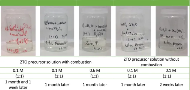
Tin chloride and zinc nitrate solutions in MP were prepared separately to analyze their stability. A solution of tin acetate in MP was also prepared to try to replace tin chloride and make the solution 100% eco-friendly, not only by replacing the solvent but also eliminating the chlorides that also contribute to the toxicity of the solution.
As can be seen from Figure 3.1, zinc nitrate solutions remain stable, keeping transparent, but the tin chloride were whitish, which indicates the deposition of precursor in the bottom, meaning that a reaction was initiated and hydroxides were formed. The tin acetate solution turned yellow indicating that the tin acetate did not dissolved in MP so it is not a good solution.
It was noticed that the tin chloride solution was transparent immediately after the dissolution, turning white only a few moments later. Based on this, that solution was added to the zinc nitrate solution immediately to avoid the formation of hydroxides. To make this test a ZTO precursor solutions with and without combustion were made, with (1:1) and (2:1) ratio, respectively, with 0.1 M concentration (Figure 3.2).
(a) (b)
Figure 3.2- (a) Solution with combustion (1:1) and (b) Solution without combustion (2:1)
(a) (b)
Figure 3.1- (a) Tin chloride solutions, (b) Zinc nitrate solution in MP and (c) tin acetate in MP solution (c)
Printing of eco-friendly solution based zin-tin oxide for device applications
10
It is observed in Figure 3.2 that the solution with combustion in the ratio (1:1) and the solution without combustion in the ratio (2:1) were both stable with a 0.1 M concentration.
3.1.2. Aging of the solutions
Aging of solutions were evaluated to see if they remain stable over time and results are shown in Table 3.1. Table 3.1- ZTO precursors solutions over time
ZTO precursor solution with combustion ZTO precursor solution without combustion
0.1 M 0.1 M 0.6 M 0.1 M 0.1 M
(1:1) (1:1) (1:1) (2:1) (1:1) 1 month and 1
week later 1 month later 1 month later 1 month later 2 weeks later Based on the Table 3.1 it can be observed that these solutions must be stable over time, even after one month as these remain transparent, which indicates that no reaction occurred.
3.1.3. Viscosity of solutions
The viscosity of the solutions was changed by the increasing the ZTO ink concentration with a molar proportion (1:1) with and without combustion. The results obtained are represented in Figure 3.3.
Printing of eco-friendly solution based zin-tin oxide for device applications
11
There is an exponential increase of the viscosity with the concentration for both solutions. The solution with combustion has a higher viscosity than the solutions without combustion, this was expected because the solution with combustion has more salts dissolved (urea and ammonium nitrate).
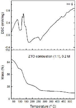
3.1.4. Thermal characterization of solutions
The DSC-TG technique were performed to investigate the decomposition behavior of the metal oxide precursors. This thermal analysis was made for ZTO with combustion, (1:1) ratio, with 0.2 M concentration. The obtained results are shown in Figure 3.4.
In Figure 3.4 two endothermic peaks are observed at 80 °C and 128 °C where there is an abrupt mass loss indicate the solvent evaporation occurs. At 170 °C there is an exothermic peak where the combustion reaction of the organic fuel with the metal nitrates occurs, when energy is released. At 260 °C an endothermic peak is noted accompanied by a mass loss, this is attributed to the degradation of residual organics. This analysis indicates that 200 °C is the temperature required for the ZTO formation reaction to occur.
3.2. ZTO thin films characterization
Several techniques were used to characterize the films. To determine film thickness, composition, transparency and crystallinity.
3.2.1. Fourier Transform Infra- Red (FTIR) spectroscopy
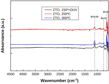
To confirm the occurrence of the reaction, the formation of zinc tin oxide and the absence of organic substances, FTIR analysis of the films was performed. A film of solution with combustion (1:1) with 0.1M concentration was analyzed, this film had a 250 °C and 300 °C annealing treatment for 30 minutes and a film of solution with combustion (1:1) with 0.2M concentration that had a 150 °C + DUV annealing
Figure 3.4- TG-DSC analysis of a ZTO precursor solution with combustion (1:1), with 0.2 M concentration
Printing of eco-friendly solution based zin-tin oxide for device applications
12
treatment for 30 minutes was also analyzed. All the films were deposited on silicon substrates. The results obtained are presented in Figure 3.5.
4500 4000 3500 3000 2500 2000 1500 1000 Zn-O Sn-O Si-O-Si Ab s o rv a n c e ( a .u .) Wavenumber (cm-1) ZTO, 150º+DUV ZTO, 250ºC ZTO, 300ºC
Figure 3.5- FTIR spectra for ZTO thin films produced from different precursor solutions.
The results are identical between regardless of different annealing treatments (250 °C, a 300 °C and 150 °C + DUV). In all of them there is no longer organic substances, because these would present a peak round to 3500 cm-1, and in this zone of the graphic no peak is observed. [28]
The peak observed at 1100 cm-1 represents the silicon-oxygen bond, this peak is related to the native SiO 2
layer on the silicon substrate that reacts with the oxygen from the air. [29] At about 750 cm-1 there is a
peak which is relative to Sn-O vibration and a peak at 600-1 which represents the Zn-O vibration. [30] So it
can be concluded that the reaction was successful even at low temperature.
3.2.2. Optical characterization
UV/VIS spectrophotometry
The use of transparent electronics is increasing and is more and more important to be able to make transparent devices. Optical characterization of the films was performed using a UV/VIS spectrophotometer. Solution combustion synthesis based ZTO (1:1) films with a 300 °C and a 150 °C + DUV annealing treatment for 30 minutes were deposited on a glass substrate and analyzed. The obtained data are shown in Figure 3.6.
Printing of eco-friendly solution based zin-tin oxide for device applications
13
From the graphic it is possible observe that both the films are transparent with 90 % transmittance in the visible light range. [31] It is also possible observe that the radiation is transmitted below 300 nm which means that the ZTO film absorbs the UV radiation.
Spectroscopic ellipsometry
In order to determine the thickness and the band gap energy (Eg) values of the ZTO films, ellipsometry
technique was performed using the Tauc Lorentz2 model. The films produced from different combustion ZTO (1:1) precursor solutions by varying solution concentration, number of layers and annealing treatment were analyzed. The results obtained of thickness and of Eg can be found in Table 3.2.
Table 3.2- ZTO thin films thickness and band gap energy determined by spectroscopic ellipsometry.
ZTO 1:1, 2-layers, 0.1M, 300 °C ZTO 1:1, 2-layers, 0.1M, 250 °C ZTO 1:1, 1-layer, 0.2M, 150 °C + DUV Thickness (nm) 22.2 23.2 28 Eg (eV) 3.39 3.68 3.56
Observing the variation of the thickness values it is possible observe that with the decrease of temperature the thickness increases slightly because with higher temperatures the film becomes denser and more condensed. The band gap energy remains approximately constant with temperature.
3.2.3. Structural characterization
To get a film with good features like the ones mentioned earlier, it must be amorphous. Previous published results show that ZTO films that took 300 °C annealing treatment are amorphous (see Annex 2A). [9] To confirm if the film deposited was amorphous after a DUV treatment the XRD technique was used. The analyzed film was made from the ZTO precursor solution with combustion (1:1) with 0.6M concentration and with a 150 °C + DUV annealing treatment during 30 minutes, deposited on silicon substrate. The obtained results can be found in the Figure 3.7.
10 20 30 40 50 60 In te n s it y ( a .u .) Angle (degrees) ZTO, 150ºC + DUV
Figure 3.7- XRD spectrum of ZTO thin film
Observing the graphic no significant peak is noticed in the curve. It can be conclude that the film is amorphous as desired. With the annealing treatment and the DUV the reaction occurred and the zinc tin oxide was formed. Otherwise there were peaks in the spectrum as can be seen in Annex 2B.
Printing of eco-friendly solution based zin-tin oxide for device applications
14
3.3. Electrical characterization of ZTO devices
TFTs and Schottky diodes were produced with solution based ZTO and their electrical behavior was characterized.
3.3.1. TFTs
The TFTs were fabricated on Si/SiO2 substrates by depositing 2 layers of ZTO solution with 0.1M
concentration using (1:1) and (2:1) proportions and using two methods, with combustion and without combustion precursor. The annealing treatment was 30 minutes at 300 °C. The deposited contacts are aluminum. The VD used was 20 V and the VG was from -10 V to 20 V. The conditions that shows good results
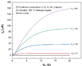
were (2:1) ZTO without combustion and (1:1) ZTO with combustion. The transfer or input curves and output curves of TFTs were analyzed. The obtained results can be observed in Figure 3.8 and Figure 3.9.
From these curves it can be concluded that the devices have a typical TFT behavior because for negative VG the passing current between the drain and source (IDS) is too low and from a certain voltage (near to
zero) the current that passes increase. From transfer curves it is possible determine the characteristic device parameters; Von, SS (equation 1.5), µSAT (equation 1.4) and on/off ratio. These values are presented
in Table 3.3. From the output curve it is possible distinguish the two regimes: triode region and saturation Figure 3.9- IV Output curve of TFTs produced by ZTO precursor solution 0.1M
concentration, on Si/SiO2 wafer.
(a) (b)
Figure 3.8- IV transfer curves of TFTs produced by ZTO precursor solution 0.1 M concentration (a) without combustion (2:1) (inset photograph of the TFTs produced) and (b) with combustion (1:1) on Si/SiO2 wafer.
Printing of eco-friendly solution based zin-tin oxide for device applications
15
region. The condition with the solution with combustion (2:1) was also tested but the devices did not show good performance (see Annex 3A).
Table 3.3- Characteristic parameters of a TFT produced by ZTO precursor solution 0.1M concentration without combustion (2:1) and with combustion (1:1)
Conditions VON (V) SS (V/dec) µSAT (cm2/V.s) On/off Ratio
Without
Combustion (2:1) -1 ± 0.6 0.36 ± 0.11 2.98 ± 0.05 1.38×10
7
With Combustion
(1:1) 0.14 ± 1.9 0.36 ± 0.12 1.24 ± 0.32 7.58×10⁶
These values prove that the TFTs have a good behavior, they have an on voltage near zero and a high on/off ratio. Ideally the SS values must be low, between 0.07 V and 0.1 V, for fast switching. These values are above the indicated but still low. When the SS values are too high it may indicate a charge leak. [18] The saturation mobility is also not to low which improves device behavior.
Is also noted that in devices made from the solution with combustion (1:1) there is a higher hysteresis and the devices made from solution without combustion (2:1) are more stable due to the fact that in the solution with combustion there is an excess of fuel due to the presence or urea, causing more film defects. These devices show equivalent performance to the current state-of-the-art of ZTO devices produced with 2-ME which is very positive, eliminating the toxic solvent, and remain the good results. [9]
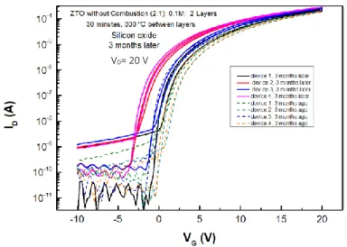
To evaluate the stability of these devices they were tested three months later to see if their behavior was maintained and if they are stable over time.
This test was performed on the TFTs with the best behavior: solution without combustion (2:1), 0.1M concentration, 2 layers and with an annealing treatment of 30 minutes at 300 °C between layers. The used VD was 20 V and the VG was from -10 V to 20 V. Figure 3.10 shows the obtained results and Table 3.4 shows
the characteristic parameters of these TFTs
Table 3.4- Characteristic parameters of a TFT produced by ZTO precursor solution 0.1M concentration, without combustion (2:1), after 3 months
Conditions VON (V) SS (V/dec) µSAT (cm2/V.s) On/off Ratio
Without combustion (2:1), 0.1M, 2 layers,
300℃
-2.5 ± 1 2.52 ± 0.54 3.0 ± 0.1 1.19×10⁷
Figure 3.10- IV transfer curves of TFTs produced by ZTO precursor solution without combustion (2:1), 0.1M concentration, on Si/SiO2 wafer, after 3 months
Printing of eco-friendly solution based zin-tin oxide for device applications
16
It is noticed that VON suffered a slight shift to more negative potential values and the SS increases but these
are minor differences because the mobility and the on/off ratio remain high which proves that these devices remain stable over time.
The annealing treatment of 30 minutes at 250 °C between layers was also tested, the results were not so good as can be seen in Annex 3B, showing a low mobility.
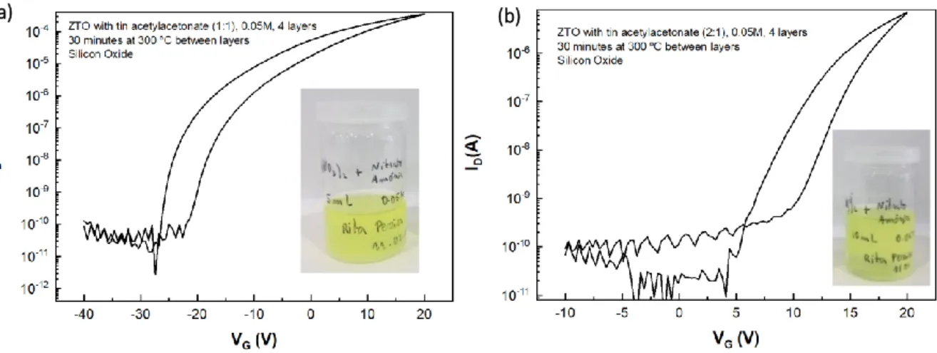
In the context of the SuperSmart project a Cl-free solution was tested for devices fabrication. In this solution tin chloride was replaced by tin acetylacetonate. This eliminates the chlorides from solution which makes it less toxic. The TFTs were produced using this solution, with 0.05M concentration, with 4 layers due their smaller concentration, with an annealing treatment of 30 minutes at 300 °C between layers. Figure 3.11 and Table 3.5 show the obtained results.
Table 3.5- Characteristic parameters of TFTs produced with Cl-free ZTO precursor solution, 0.05M concentration, on silicon oxide
Using a non-toxic solvent and a Cl-free ZTO precursor solution TFTs with good performances were successfully produced. With the (1:1) ratio the on voltage is very negative but it has a good on/off ratio and good mobility. With the (2:1) ratio has also a good performance and the on voltage is near zero so this is a good condition to make TFTs. However these devices have a difficult stabilization as can be seen in Annex 3C.
3.3.2. Schottky diodes
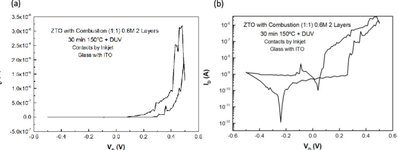
Schottky diodes were produced on commercial ITO covered glass substrates. The devices that show best results were made from solution with combustion (1:1), 0.6M concentration, with 2 layers and with a annealing treatment of 150 °C + DUV during 30 minutes between layers. The other results can be observed in Annex 4A. The used VG was from -0.8 V to 1 V. The top Ag contact were deposited by thermal evaporation
via shadow mask. In this case Ag are used for the contacts due its work function that is higher than in the aluminium and lead to better diodes.
Figure 3.12 shows the obtained results.
Ratio VON (V) SS (V/dec) µSAT (cm2/V.s) On/off Ratio
(1:1) -27.4 1.38 1.49 1.3 × 10⁸
(2:1) 4.1 0.63 1.44 7.4× 10⁵
(a) (b)
Figure 3.11- IV transfer curves of TFTs produced with Cl-free ZTO precursor solution without combustion (a) (1:1) and (b) (2:1), 0.05M concentration, on Si/SiO2 wafer.
Printing of eco-friendly solution based zin-tin oxide for device applications
17
The characteristic rectifying behavior of such a diode is verified, where to negatives voltages the passing current is too low and from a certain voltage (VON) the current increase. This device presenting a VT of 0.7
V and a current on/off ratio of 800.
On the same substrate, Ag contacts were printed by inkjet determine the influence of the top contact deposition technique. The used VG was from -0.5 V to 0.5 V. Figure 3.13 shows the obtained results.
A smaller voltage was applied on this diodes due to the contacts area which on these devices is smaller. The rectifying behavior of diode remains which demonstrates that the contacts can be deposited by Inkjet. However the obtained curves by inkjet are less smooth because of the interface between the contact and the semiconductor, when the contact is deposited by ebeam this interface have more quality due to this technique is performed in vaccum instead of inkjet technique that is performed in an environment that does not favor the quality of the interface. But anyway this device presenting a VT of 0.3 V and a current
on/off ratio of 1000 which are interesting results that proves that the inkjet printing is a good alternative to the ebeam to deposit the contacts.
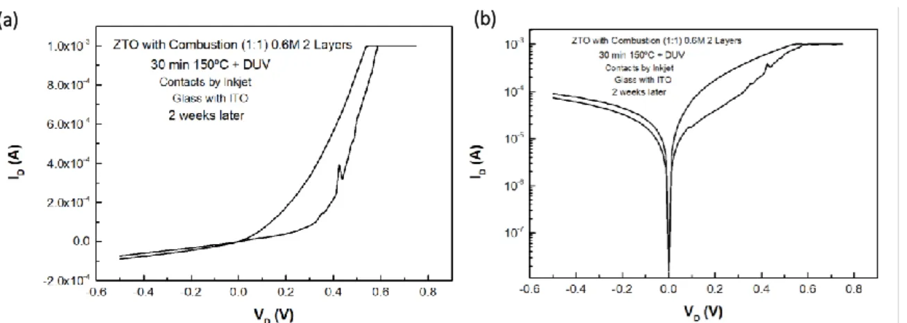
To verify if ZTO precursor solutions remains stable over time a two weeks aged (1:1) solution combustion was tested due the best results. 2 layers were deposited with a 150 °C + DUV annealing treatment for 30 minutes between layers. The used VG was from -0.5 V to 0.8 V. The Ag contacts were deposited by inkjet.
Figure 3.14 show the obtained results.
(a) (b)
Figure 3.12- IV curves of diodes produced by ZTO precursor solution with combustion (1:1), 0.6M concentration, on glass with ITO, with contacts deposited by thermal evaporation, (a) linear scale (inset photograph of the Schottky diodes produced) and (b) logarithmic scale
(a) (b)
Figure 3.13- IV curves of diodes produced by ZTO precursor solution with combustion (1:1), 0.6M concentration, on glass with ITO, with contacts deposited by Inkjet. (a) Linear scale and (b) logarithmic scale.
Printing of eco-friendly solution based zin-tin oxide for device applications
18
It is possible observe the behavior of the diode, however presenting a VT of 0.36 and a current on/off ratio
of 10.3. It can be noticed a clear decrease in its performance, the on/off ratio decreases two orders of magnitude. It can be conclude that the solution loses some quality over time. The 3 week test also was made, presenting a worst performance than 2 week. The results can be observed in Annex 4B.
Diodes were also produced using a non-toxic Cl-free ZTO precursor solution, with 0.6M concentration, with 2 layers. Two annealing treatments were tested: 30 minutes at 150 °C + DUV between layers and 30 minutes at 250 °C in HP between layers. The Ag contacts were deposited by thermal evaporation. Figure 3.15 and Table 3.6 shows the obtained results. The used VG was from -1 V to 1 V or to 2 V.
.
(a) (b)
Figure 3.14- IV curves of diodes produced by ZTO precursor solution with combustion (1:1), 0.6M concentration, on glass with ITO, with contacts deposited by Inkjet, 2 weeks later. (a) Linear scale and (b) logarithmic scale.
(a.1)
(b.1)
(a.2)
(b.2)
Figure 3.15- IV curves of Schottky diodes produced by ZTO precursor solution, where tin chloride was replaced by tin acetylacetonate, 0.6M concentration, on glass with ITO, contacts deposited by Ebeam. (a.1) and (a.2) with an annealing treatment at 250 °C in HP in linear and logarithmic scale respectively and (b.1) and (b.2) With an annealing treatment at 150 °C + DUV in linear and logarithmic scale respectively.
![Figure 1.3- Energy band diagram of an ideal TFT for different bias conditions [13]](https://thumb-eu.123doks.com/thumbv2/123dok_br/15582052.1049368/25.892.281.581.514.690/figure-energy-band-diagram-ideal-tft-different-conditions.webp)