Nuno Miguel Gonçalves Pinela
Licenciado em Ciências da Engenharia de Micro e Nanotecnologias
Piezoresistive pressure sensor for application in
e-skin devices
Dissertação para obtenção do Grau de Mestre em
Engenharia de Micro e Nanotecnologias
Orientador: Doutor Rui Alberto Garção Barreira do Nascimento Igreja, Professor auxiliar, Faculdade de Ciências e Tecnologia da Universidade Nova de Lisboa Co-orientador: Doutor Hugo Manuel Brito Águas,
Professor auxiliar, Faculdade de Ciências e Tecnologia da Universidade Nova de Lisboa
Júri
Presidente: Doutor Rodrigo Ferrão de Paiva Martins Arguente: Doutor Carlos Jorge Mariano Miranda Dias
Vogal: Doutor Rui Alberto Garção Barreira do Nascimento Igreja
Piezoresistive pressure sensor for application in e-skin devices
Copyright © Nuno Miguel Gonçalves Pinela, Faculdade de Ciências e Tecnologia, Univer-sidade NOVA de Lisboa.
A Faculdade de Ciências e Tecnologia e a Universidade NOVA de Lisboa têm o direito, perpétuo e sem limites geográficos, de arquivar e publicar esta dissertação através de exemplares impressos reproduzidos em papel ou de forma digital, ou por qualquer outro meio conhecido ou que venha a ser inventado, e de a divulgar através de repositórios científicos e de admitir a sua cópia e distribuição com objetivos educacionais ou de inves-tigação, não comerciais, desde que seja dado crédito ao autor e editor.
Este documento foi gerado utilizando o processador (pdf)LATEX, com base no template “novathesis” [1] desenvolvido no Dep. Informática da FCT-NOVA [2].
Acknowledgements
I would like to acknowledge everyone who contributed for this master thesis to hap-pen and to be concluded, starting from Professor Rodrigo Martins and Professor Elvira Fortunato, who have developed these two multidisciplinary research centers, which are CENIMAT|i3N and CEMOP, where I have spent my last nine months and where I found all the tools to surpass barriers and acquire knowledge. I would also like to show my acknowledgement to this great institution, FCT-UNL, where I find myself growing and evolving everyday, since the first day I joined it.
Secondly, I would like to express my gratitude to Professor Rui Igreja, for accepting and introducing me to this wide world of sensors. Furthermore, I would like to thank for the guidance and orientation in every single meeting. I am also grateful to Andreia, who has supported me and contributed significatively for this thesis. To Professor Hugo Águas, I also want to thank for the guidance.
Moreover, I want to thank CENIMAT|i3N members Alexandra Gonçalves, Sónia Pereira, Ana Carolina Marques, Ana Samouco, Beatriz Coelho, Ricardo Ferreira, Tiago Mateus, Rodrigo Santos, Pedro Alves, Daniela Gomes and Tomás Calmeiro, who have always provided me the help I needed, in terms of suggestions, logistics and technical support.
To all my friends from Open-Space, I want to give special thanks because in spite of our duty to complete this hard task of writing a master thesis, we managed to have fun and to help each others in one or another situation.
To my course friends who have been these last five years with me, João Afonso, Marco and Shiv. To my friend Tiago Gameiro, I would really like to express my gratitude, for the good times we have spent during these years. To my long-time friends Alexandre Ferrão, Gonçalo Félix and Duarte Pais, who have been an important support. Also, I want to thank to my girlfriend’s family for the support.
I want to specially acknowledge all my family. To my grandparents for all the pride they put on me. To my parents Anabela and António, for conceding me this opportunity of education. I will be forever grateful, and will always praise on follow the principles I have been taught. To my brother Pedro, who has been a major pillar throughout the years. I also want to thank Noa for the unconditional love. To Mariana, who has made this walk alongside me, making it much easier. A few lines here would not be enough to express how thankful I am for all the love, support, motivation and for everything she is.
Abstract
In recent years, the advancement of science and technology tends to evolve towards the exploitation of electronic skin (e-skin) and functional prosthetic devices, enabling inno-vating applications in various fields such as biomedical systems, sports health-monitoring and healthcare. Owing to their significant role in health monitoring, pressure sensors come as essential components in the development of artificial systems that can mimic the impressive human skin. The development of such sensors comprises the search for flexi-ble and stretchaflexi-ble materials suitaflexi-ble for implementation in robust devices that enaflexi-ble the integration of multiple sensing-functionalities. To quantitatively monitor pressure, these sensors use transduction methods based on piezoresistivity, capacity, piezoelectric-ity, and triboelectricity.
In this work, piezoresistive devices were chosen over others due to their ease in struc-ture design and readout mechanism. The mechanism of such piezoresistive pressure sensor relies on the transduction of a pressure change into a change in resistance that, in this case derives from variations in the contact area.
In the approach presented in this work, a semi-sphere microstructuring pattern-ing made by laser engravpattern-ing onhard-poly(dimethylsiloxane) (h-PDMS)was introduced.
h-PDMS works as a mold from which standard-poly(dimethylsiloxane) (s-PDMS) mi-crostructured membranes with approximately 200 µm thickness are peeled off.
Carbon-ink, working as active material, was deposited on top of the microstructured s-PDMS
membranes. The fabrication of such pressure sensors based on organic membranes com-bines advantages such as the production in a low-cost and fast way, device flexibility, and tunability of the sensor’s design. Moreover, sensitivities of 2.4×10⁻¹kPa−1were reached
for the sensors developed.
Keywords: Electronic skin, piezoresistivity, microstructures, semi-spheres, PDMS.
Resumo
Nos últimos anos, o avanço da ciência e da tecnologia tende a evoluir para a exploração da pele eletrónica (e-skin) e próteses funcionais, possibilitando aplicações inovadoras em vários campos, nomeadamente sistemas biomédicos, saúde desportiva, e monitoriza-ção da saúde. Devido ao seu papel significativo na monitorizamonitoriza-ção da saúde, os sensores de pressão são componentes essenciais no desenvolvimento de sistemas artificiais que conseguem imitar a impressionante pele humana. O desenvolvimento destes sensores requer a procura por materiais flexíveis e extensíveis adequados para implementação em dispositivos robustos que permitam a integração de múltiplas funcionalidades de detec-ção. Para monitorizar a pressão, estes sensores usam métodos de transdução baseados em piezoresistividade, capacidade, piezoelectricidade e triboeletricidade.
Neste trabalho, dispositivos piezoresistivos foram escolhidos em detrimento dos ou-tros devido à sua fácil implementação e mecanismo de leitura. Este mecanismo consiste na transdução de uma diferença de pressão numa diferença de resistência que, neste caso, deriva de variações na área de contato.
Na nova abordagem apresentada neste trabalho, introduziu-se um método de micro-estruturação de semi-esferas baseado na gravação a laser em poli(dimetilsiloxano)-duro (h-PDMS). O h-PDMS funciona como um molde a partir do qual se retiram membranas microestruturadas de poli(dimetilsiloxano)-standard (s-PDMS) com aproximadamente 200 µm de espessura. O material ativo em cima do domínio microestruturado é tinta de carbono. A fabricação destes sensores de pressão com base em membranas orgânicas com-bina vantagens como a produção de forma rápida, fabricação de baixo custo, flexibilidade do dispositivo e flexibilidade na mudança do design do sensor. Para além disso, para estes sensores foram conseguidas sensibilidades de 2.4×10⁻¹kPa−1.
Palavras-chave: Pele electrónica, piezoresistividade, microestructuras, semi-esferas, PDMS.
Contents
List of Figures xv
List of Tables xvii
Acronyms xix
Motivation and Objectives xxi
1 Introduction 1
1.1 Electronic Skin . . . 1
1.2 Pressure Sensor Fundamentals . . . 1
1.3 Piezoresistive pressure sensor devices. . . 3
1.3.1 Substrate Materials . . . 4
1.3.2 Active Materials . . . 5
2 Materials and Methods 7 2.1 Chemicals and Materials . . . 7
2.2 Fabrication and laser engraving of PDMS molds . . . 7
2.3 Fabrication of the piezoresistive pressure sensor devices . . . 8
2.4 Morphological characterization of microstructured PDMS films. . . 9
2.5 Characterization of carbon-coated membranes. . . 9
2.6 Electrical characterization of devices . . . 10
3 Results and Discussion 11 3.1 Patterning . . . 11
3.2 Ink Study . . . 18
3.2.1 Carbon-ink dilution study . . . 18
3.2.2 Ink layers study . . . 19
3.2.3 Electrical Characterization of carbon-coated membranes . . . 20
3.2.4 Morphological Characterization of carbon-coated membranes . . 20
3.3 Homemade Pressure Applying System . . . 22
3.4 Electrical Characterization of Devices. . . 25
4 Conclusions and future perspectives 29
Bibliography 31
A Semi-sphere’s dimensions measurements 37
B I-V tests 39
C Coated-PDMS microstructures measurements 41
C O N T E N T S
D Pressure applying system 43
E Sensor operation principle 47
F Resistance changes for different frequencies 49
G Estimated sensor price 51
List of Figures
1.1 Two main strategies to fabricate devices with improved stretchability . . . . 3
2.1 Schematic showing the principle steps of pressure sensors conception. . . 8
2.2 Photograph showing the bendability/flexibility of (a) one microstructured membrane that was peeled offfrom a h-PDMS mold. (b) the fabricated device 8 3.1 SEM images acquired from a top view of peeled membranes from molds made in s-PDMS in vector mode . . . 12
3.2 Semi-Spheres height versus Laser Power . . . 14
3.3 Real Diameter versus Designed Diameter . . . 16
3.4 Real pitch versus Designed Pitch . . . 16
3.5 Molds produced for fabrication of membranes. . . 17
3.6 Microscope acquired images of the fabricated molds. . . 17
3.7 Sheet resistance of smooth carbon-coated PMDS and PMMA-coated PDMS for four different carbon-ink dilutions in water. . . 18
3.8 Number of carbon coating layers study. . . 19
3.9 Block diagram representing the blocks constituting the system built. . . 22
3.10 Circuit design for the development of the system. . . 23
3.11 Picture representing the pressure apllying system developed. . . 24
3.12 Pressure applied on piezoelectric sensor versus time. . . 25
3.13 Voltage sweep from -2 to 2 V proving the ohmic behaviour of two devices . . 26
3.14 Resistance changes in response to applied pressure over time . . . 27
3.15 Resistance response to different pressures. . . . . 28
B.1 Voltage sweep from -2 to 2 V proving the ohmic behaviour of four membranes. 39 D.1 Schematic representation of the developed system. . . 44
D.2 Sketch in SketchUp of component 1 of the homemade system. . . 45
D.3 Sketch in SketchUp of components 2 and 3 of the homemade system. . . 45
D.4 Sketch in SketchUp of component 4 of the homemade system. . . 45
D.5 RC Low-Pass Filter with Op Amp Buffer. . . 46
E.1 Sensor operation principle based on resistance changes in responses to loading and unloading. . . 47
F.1 Resistance changes in response to an applied pressure . . . 49
List of Tables
1.1 State of the Art of piezoresistive pressure sensors . . . 4
3.1 Membranes peeled offfrom molds fabricated in s-PDMS using three different
designs . . . 11
3.2 Membranes peeled offfrom molds fabricated in h-PDMS using laser engraving
in raster mode, power of 50 W, and a speed of 0.762 m/s. . . 13
3.3 Summary of height measurements of semi-spheres using different
combina-tions of designed base diameters and laser powers. . . 14
3.4 SEM images acquired of microstructured PDMS films. . . 15
3.5 SEM images of microstructures produced on PDMS with carbon or PMMA + carbon coatings. . . 21
A.1 Semi-spheres real diameter and real pitch measured on horizontal and vertical directions . . . 37
C.1 Measurements of dimensions of the fabricated microstructures with carbon coating and with carbon coating with PMMA. . . 41
G.1 Estimated sensor price regarding materials costs . . . 51
Acronyms
CNTs carbon nanotubes.
h-PDMS hard-poly(dimethylsiloxane).
LCD liquid crystal display.
LOD limit of detection.
PDMS poly(dimethylsiloxane).
PEDOT:PSS poly(3,4-ethylenedioxythiophene) polystyrene sulfonate.
PEN polyethylene.
PI polyimide.
PMMA poly(methyl methacrylate).
PVDF poly(vinylidene) difluoride.
PZT lead zirconate titanate.
SEM scanning electron microscope.
s-PDMS standard-poly(dimethylsiloxane).
Motivation and Objectives
Nowadays, the pursuit for information-sensing inspired by human skin has been moti-vated by the possibility of application on functional health monitoring systems and on robotic systems. Therefore, in order to achieve this, thin film pressure sensors are being widely exploited.
Furthermore, efforts have been made towards the fabrication of thin film sensors in
a non-clean room environment, which would considerably lower the device cost. Thus, the main goal of this work is to design, fabricate and develop low-cost, flexible pressure sensors based on the piezoresistive effect, which could be easily adapted and conformed
to different surfaces, using microstructured substrates.
Large scale production greatly benefits from low manufacturing costs in flexible pres-sure sensors, and the simplification of the device’s structure and manufacture is also desirable. These piezoresistivity-based devices allow an easy readout mechanism, as well as a simple structure design, which in turn will allow an easy device optimization. More-over, through the use of the perfect combination of materials one expects to produce each sensor for approximately 0.351€(materials costs).
Finally, the fabricated materials will be extensively characterized, both morphologi-cally and electrimorphologi-cally, as to compare different designs, with the primary goal of developing
a sensor with the best sensitivy possible.
C h a p t e r
1
Introduction
1.1 Electronic Skin
Human skin is an outstanding organ, being our interface with the surrounding world and allowing us to perceive mechanical stimuli such as pressure, shapes and textures [1]. This sense of information is only achievable because human skin comprises mechanoreceptors that receive a mechanical stimulus which is than transduced into a biological response [2]. Nowadays, inspired by this illusory simplicity of nature, efforts are being made to develop
skin-inspired electronic devices. The pursuit for these e-skin devices is motivated by the possibility of application on functional prosthetic devices [3], humanoid robotics [4] and human health monitoring, where it could play a key role [5, 6]. Therefore, accurate quantitative monitoring requires an effective transduction where transduction
mecha-nisms such as piezoresistivity [7–9], capacitance [10–12], piezoelectricity [13–15], and triboelectricity [16–18] are being widely exploited to develop different types of pressure
sensors.
1.2 Pressure Sensor Fundamentals
Firstly, for a better comprehension of pressure distributions, pressures such as human touch, object manipulation, and human body circulation are considered to be in the low pressure (<10 kPa) and medium-pressure (10-100 kPa) regimes [12]. Secondly, and given that a pressure sensor transduces a mechanical pressure into an electrical signal an outline of some noteworthy key parameters that include sensitivity, limit of detection (LOD), linearity, response time and stability is presented. Among these, sensitivity, which is defined by the ratio between the variation of the quantitative output signal and variation of the applied pressure, is one of the most important parameters because it defines the accuracy and effectiveness of the measurement [19]. Sensitivity is defined as
S= ∆R
R0
!
∆P (1.1)
WherePdenotes the applied pressure and∆R/R0is the relative resistance change of the sensor.
LODrepresents the lowest quantity of pressure that can be distinguishable. Lowering the LOD of a pressure sensor represents an improvement on lower pressure detection which is a requirement in lower pressure regimes [20].
Another relevant parameter is linearity, which is a classification expressed as percent-age of the deviation of the sensor’s output curve from a specified straight line over a
C H A P T E R 1 . I N T R O D U C T I O N
certain pressure range [20]. Hence, one desires to have pressure sensors with broad linear ranges, which simplifies the conversion of mechanical pressure into electrical output.
Response time can be defined as the time required for a pressure sensor output to go from its previous state to a final stable value [20]. This parameter is especially important in dynamic real-time pressure sensing devices, when producing real-time monitoring systems or instant-response displays.
Furthermore, to accurately measure the magnitude of a pressure stimulus, the most relevant transduction methods are piezoelectricity, capacitance, and piezoresistivity .
Piezoelectricity, which is the ability (quantified by the piezoelectric strain constant d33) of a material to generate electrical charges in response to the occurrence of electrical dipole moments due to applied mechanical stresses. This property of crystals and certain ceramics is good for development of low-power-consumption or self-powered sensing devices [21]. Moreover, the piezoelectric element of the device can be combined with transistors to improve sensitivity [13]. The development of piezoelectric pressure sensors has been receiving lots of attention due to their fast response speed and self-powered oper-ation. The piezoelectric materials most used for this application includepoly(vinylidene) difluoride (PVDF)and its copolymers,lead zirconate titanate (PZT)[13], and Zinc Oxide (ZnO) [22].
Capacitive sensor transduction consists of a change in capacitance caused by the deflection of the plate when an external stimulus is applied. As dielectric constant (per-mittivity) of the medium between the plates is a constant, the external stimulus, either an applied pressure or shear force, usually represents a change in area or in the distance between the plates, respectively [1].
Capacitive sensors offer advantages such as high sensitivity, but the main advantage
of this types of sensors is the simplicity of their governing equation, which allows a direct analysis and a simple device design [23]. These sensors have also demonstrated the characteristic of high strain sensitivity for detection of a static force with low-power consumption [24]. However, once capacitance is proportional to the area, a reduction in the size of these devices for miniaturization means a reduction of the capacitance and the signal-to-noise ratio [25]. Additionally, capacitive sensors are vulnerable to external interferences [26].
The other transduction method commonly used is based on piezoresistive effect.
Piezore-sistive sensors have been widely investigated due to their simple structure and readout mechanism [27]. These sensors transduce a force variation into changes in resistance of a device that is detected by an electrical measuring system. The resistance variation de-rives most commonly from changes in: the geometry of the sensing element; the contact resistance (RC) and the resistivity of a composite due to changes in separation between particles. Usually, for these type of sensors, when the resistivity of the material is constant, a change in resistance derives from changes in the geometry of the sensing element.
For conductive materials, the mechanism relies on changes in the RC between both materials. A RC change caused by change in contact area between two conductors is
1 . 3 . P I E Z O R E S I S T I V E P R E S S U R E S E N S O R D E V I C E S
proportional to the square root of the force, which is an advantage as it provides high sen-sitivity at lower pressures as well as it expands the usable range [1]. For conductive elastic composites, piezoresistance depends on the morphology, composition, and strain range of the system, and the mechanism relies on changes in conductive path. Furthermore, piezoresistive sensors exhibit a fast response speed [1]. However, piezoresistivity-based sensors usually show undesirable drift and hysteresis [28].
As seen, the presented transduction methods provide different sensing capabilities
which allows systems to integrate multifunctional sensors. For example, piezoresistive are usually used to reliably measure large strains [29], capacitive devices to sense normal forces and piezoelectric devices to measure vibrations [1].
1.3 Piezoresistive pressure sensor devices
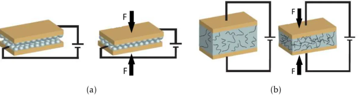
Being human skin considered as a performance benchmark for the development of e-skin, some considerations need to be followed to grant this electrical material the mechanical properties of human skin, such as stretchability, flexibility, and low Young’s modulus [1]. To fulfil these considerations, the design and fabrication of the device are critical. An important parameter is regarding device’s stretchability and there are two main strategies used to improve it [30]. The first method (Figure1.1a) uses a thin conductive material bonded to an elastic substrate, such aspoly(dimethylsiloxane) (PDMS)[10]. The second method (Figure1.1b) is based on the fabrication of devices by mixing conductive materials into an elastomeric matrix [31].
F
F
(a)
F
F
(b)
Figure 1.1: (a) Thin conductive material bounded to a micro-structured elastomer. (b) Mixture of a conductive material on an elastomeric matrix.
Another important parameter in pressure sensors design is the contact area, which can be increased by constructing various device geometries, for example through the materials microstructuration. Creating the desired geometry requires techniques such as lithography [32], coating [33], and micro-channel molding and filling [34]. This concept has shown to be an ideal candidate for e-skin applications [8,12]. For this reason, and to be able to meet the needs stated above, the materials choice is crucial for the development of flexible pressure sensors and herein, an outline of substrate and active materials for piezoresistive pressure sensors is presented. Table1.1 summarizes piezoresistive pres-sure sensors developed over the recent years as well as their performance parameters, to
C H A P T E R 1 . I N T R O D U C T I O N
understand the trend in piezorestive pressure sensor development.
Table 1.1: State of the Art of piezoresistive pressure sensors. Abbreviations used in this ta-ble: Carbon Nanotubes (CNTs), Gold (Au), Gold Nanowires (AuNWs), Limit of Detection (LOD), Not Available (NA), Platinum (Pt), Poly(3,4-ethylenedioxythiophene) Polystyrene Sulfonate (PEDOT:PSS), Polydimethylsiloxane (PDMS), Polyurethane Dispersion (PUD), Single-walled Carbon Nanotubes (SWNTs), Zinc Oxide (ZnO).
Materials Sensitivity
(kPa−1)
(LOD) (Pa)
Operating Voltage (V)
Response time (ms)
[7] Pt-coated Nanohairs NA 5 NA 50
[9] AuNWs coated tissue 1.14 13 1.5 <17
[27] Polypyrrole 133.1 0.8 NA 47
[35] PDMS/SWNTs 1.8 0.6 2 <10
[36] PDMS/PEDOT:PSS/PUD 10.3 23 0.2 200
[37] PDMS/Graphene 8.5 1 1 40
[38] PEDOT:PSS/ZnO nanorods 0.00617 NA 3 30
[39] Graphene 0.034 0.3 NA 40
[40] Au-coated polymer sponge -0.31 <10 NA <10
[8] PDMS/CNT mixture -15.1 0.2 10 40
1.3.1 Substrate Materials
An e-skin pressure sensor requires flexible and stretchable substrates such asPDMS[41],
polyimide (PI)[42], andpolyethylene (PEN)[43].PDMSis a silicon-based organic poly-mer that, among other applications, has been widely used in microfluidic chip fabrication [44]. PDMSfilms are currently the flexible substrates most used to integrate sensitive materials for the fabrication of e-skin and other flexible electronic applications. This fact is due to its commercial availability and well-researched properties, namely excellent elasticity, stability over a wide range of temperatures, conformability, transparency, abil-ity to define adhesive regions for surface bonding with other materials through exposure to UV/O2irradiation [1], and biocompatibility, derived from its impermeability to wa-ter, nontoxicity to cells, and permeability to gases [35, 45]. One can realize that from the year 2014 on, the tendecy was to fabricate microstruredPDMS-based sensors. The presented sensors comprisingPDMSas substrate material show values of sensitivities in good agreement with each others and all above 1 kPa−1.
Another flexible polymer isPI, which shows excellent stability and withstands large temperature ranges, given that this material has a small linear thermal expansion coeffi
-cient [42]. In literature, other flexible pressure sensors onPIsubstrates were developed, proving the stability of this polymer and the possibility of reaching a very thin thickness, allowing small radial bending [46]. According to literature, some other less conventional materials are used as substrate such as elastomeric fibers [47] and textiles [48].
1 . 3 . P I E Z O R E S I S T I V E P R E S S U R E S E N S O R D E V I C E S
1.3.2 Active Materials
Active materials play the most important role on pressure sensor design, as these are the components responsible for granting the device its transduction properties. The most commonly reported active materials are either conductive materials or elastomer conductive composites.
Conductive materials to be used in e-skins should be low cost, present a long-time endurance, and have a good adherence on substrates. In the search for these important characteristics, conductive inks such as silver ink come as particularly attractive materials for these type of e-skin sensors as they provide the stated and also show high conductivity, while allowing great stretchability and elasticity [49]. Another example of material is graphene which is a monoatomic thin carbon film with high conductivity [50]. This material seems to be suitable to act as an active material in pressure sensors due to its mechanical and electrical properties [50].
Conductive fillers such ascarbon nanotubes (CNTs), metal particles, conductive nan-otubes and nanowires of other materials besides carbon [9], and conductive polymers such aspoly(3,4-ethylenedioxythiophene) polystyrene sulfonate (PEDOT:PSS)[36] are commonly used in elastomeric matrixes ofPDMS, sponge and other porous materials. To obtain these type of sensors, elastomers and conductive materials are mixed using appropriate methods and a ”trade-off” between mechanical elasticity and electrical
con-ductivity is a challenge because increasing concon-ductivity is commonly only achievable by increasing the amount of the conductive filler, which means a decrease in elastic-ity. CNTsare the conductive fillers most commonly used due to their high conductivity and large anisotropy, as well as chemical stability [51].CNTsin polymer matrixes have some disadvantages, as well, such as the different amount of impurities and structural
defects resultant from preparations ofCNTs, which means that it is very difficult to
pro-duceCNTswith controlled reproducibility. Another challenge is the efficient translation
of performance of a single nanotube into the performance of the system composed by the elastomer and the conductive fillers [52]. Other methods include the application of metal/metal-coated nanowires comprising a sensitivity of about 1 kPa−1 as shown on
Table1.1.
In this work the defining feature of the piezoresistive sensors was the design of the micro-structured domain on each membrane. Microstructuring the membranes results in an increase of the contact area, which affects the contact resistance, hence
increas-ing the ROFF/RON ratio [8]. Herein, and inspired by the epidermal-dermal interlocked microstructures in human skin, semi-sphere designs were explored to amplify pressure signals, as shown on (Figure 1.1a). Furthermore, semi-spheres were chosen over other geometric shapes such as cones, cylinders or square pillars due to their easy fabrication process. On top of semi-spheres, carbon-ink played the role of active material of the device, conceding it its electrical properties.
C h a p t e r
2
Materials and Methods
2.1 Chemicals and Materials
PDMSelastomer and curing agent (Sylgard 184) - Dow Corning.poly(methyl methacry-late) (PMMA) (MW approximately 120,000) and trichloro(1H, 1H, 2H, 2H- perfluo-rooctyl)silane (97%) - Aldrich. Toluene (99.99%) - Fisher Scientific. Highly conductive water-based carbon coating (PE-C-808) and water-based silver conductive ink (PE-WB-1078) - Conductive Compounds.
2.2 Fabrication and laser engraving of PDMS molds
Herein, molds made ofh-PDMSwere used. The higher Young’s modulus ofh-PDMSis important to not only achieve a high fidelity between patterns but also to easily peel off
standardPDMSmembranes, with lower Young’s modulus, from the mold [53]. Due to their lower Young’s modulus, the peeled offPDMSmembranes are designateds-PDMS.
h-PDMSmolds were fabricated by mixingPDMScuring agent toPDMSelastomer in a 1:5 w/w ratio. The mixture was then degassed in vaccum until all air bubbles had burst, and it was then dropped into a Petri dish. The Petri dish containingPDMSwas posteriorly cured for about 1 hour at 70 ºC.
Molds were microstrutured by generating micro-cavities on the surface of 5-mm-thick
h-PDMSsheets using a laser engraving machine (VLS3.50, 50 W, Universal Laser System, USA) with a carbon dioxide laser beam. This machine has a focus length of lens of 2.0 in. and the diameter of focal spot is 127 µm. Additionally, the laser engraving machine allows engraving in two different modes: vector and raster. In raster mode, the laser beam
works in a straight line, etching each line at a time. On the contrary, when working in vector mode, the laser beam acts as an inkjet printer, printing the shape approximately as it is. The micro-cavities can be achieved by melting certain spots and what defines the aspect of the cavity is the power and duration of the laser beam on the spot, which is controlled by computer, as well as their initial design. The desired patterns to be engraved were previously designed in Adobe Illustrator (2015.0.0) and exported as CAD files. These patterns consist in replicating the same geometric figure the same times over rows and columns performing a window with 2 x 2 cm2.
After fabricating these molds, they were cleaned in an ultrasonic bath for 10 min in isopropanol alcohol, followed by a rinsing in MiliQ water. In order to easily peel offPDMS
films from the engraved molds, these molds were placed in a desiccator for 30 min with 1 drop of trichloro(1H, 1H, 2H, 2H-perfluorooctyl)silane. This treatment provides the
PDMSan hydrophobic layer of trichloro(1H, 1H, 2H, 2H-perfluorooctyl)silane, allowing
C H A P T E R 2 . M AT E R I A L S A N D M E T H O D S
an easy peeling.
a. b.
e.
c.
f.
d.
g.
PDMS
PMMA
Carbon ink Silver ink
Figure 2.1: Schematic showing the main steps of pressure sensors conception. (a) h-PDMS mold (5 cm x 5 cm) being laser engraved with semi-sphere cavities. (b) s-h-PDMS spin-coating over the previously made h-PDMS mold. (c) Peeling off the flexible and
already cured s-PDMS membrane from the h-PDMS mold containing the microstructures. (d) PMMA spin-coating on PDMS membrane. (e) Carbon-ink spin coating on the PMMA-coated PDMS membrane. (f) Carbon-ink coating on the membrane after curing. (g) Representation of the fabricated device by layers, with a silver-ink stripe on the smooth edge of each micro-structured PDMS film. Note that none of the steps are at scale.
2.3 Fabrication of the piezoresistive pressure sensor devices
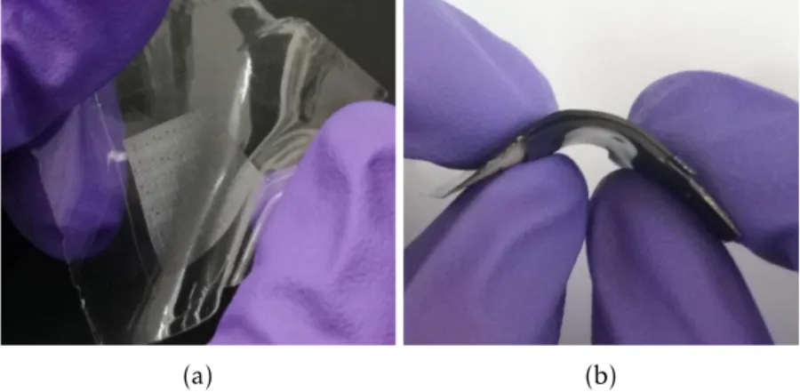
(a) (b)
Figure 2.2: Photograph showing the bendability/flexibility of (a) one microstructured membrane that was peeled offfrom a h-PDMS mold. (b) the fabricated device
For the fabrication of the microstructureds-PDMS films,PDMS was prepared in a ratio of 1:10 w/w of curing agent to elastomer and subsequently degassed in vacuum until all air bubbles had burst. PDMS was posteriorly spin-coated at 250 rpm for 90 s onto each engraved mold in quantities of 1.5 mL, ensuring the whole 5 cm x 5 cm of mold were
2 . 4 . M O R P H O L O G I CA L C H A R AC T E R I Z AT I O N O F M I C R O S T R U C T U R E D P D M S
F I L M S
uniformly covered. This process was followed by another degassing process performed for 30 min, granting the absence of bubbles in the curing process and ensuring the high fidelity betweenPDMSfilms andPDMSmolds. The curing process occurred for 30 min at 85 ºC in an Infrared IC Heater (T-962 Eco-Worthy). After curing,PDMSmembranes were easily peeled offas shown on Figure2.1, due to the silane treatment previously done on
molds surface. Figure2.2ashows a peeled offPDMSmembrane containing the designed
microstructured domain. PMDS membranes were then spin-coated at 1000 rpm for 20 s with highly conductive water-based carbon coating (PE-C-808), which plays the role of conductive material on the device. This carbon-ink coating was preceded by an O2 plasma treatment (37.5 W for 1 min with an O2 pressure of 0.3 mbar), which modifies
PDMS surface with hydroxyl groups and makes it hydrophilic, facilitating adhesion of carbon ink onPDMS. Curing the carbon ink occured for 30 min at 85 ºC, and the result is shown on Figure2.1.
To fabricate piezoresistive devices, carbon-ink-coated-membranes were then cut into the desired size (3 cm x 2 cm) and two membranes of the same pattern were sandwiched ensuring both micro-structured domains were centred with each other. Both membranes were finally sealed with 4 drops ofPDMSin each corner. To ensure the good stability of the electrodes and to improve their conductivity, lines of water-based silver conductive ink (PE-WB-1078) were deposited on the edges of each film as shown on Figure2.1. These lines were then cured at 145 ℃for 120 s. Some experiments in this work use PMMA
as a coating betweenPDMS and carbon-ink layer. PMMA(10 wt% in toluene) coating was also preceded by an O2plasma treatment (37.5 W for 1 min with an O2pressure of 0.3 mbar) and it was spin-coated onto thePDMSsurface at 1000 rpm for 60 s. Thermal curing ofPMMAfilms occured in vacuum for 1 h at 140 ºC.
2.4 Morphological characterization of microstructured PDMS
films
MicrostructuredPDMSfilms peeled from each mold were then coated with a gold/pal-ladium (Au/Pd) layer of 15 nm to 20 nm thickness in a turbo-pumped sputter coater (Quorum Q150T ES). Then, images of the films were acquired with a tabletopscanning electron microscope (SEM)(Hitachi TM3030Plus) in a standard observation mode at 15 kV using the software Hitachi TM3030Plus (01-04-02).
2.5 Characterization of carbon-coated membranes
To measure sheet resistance of membranes, Keithley 2000 Multimeter was used in a simple 2-wire configuration (as the resistance is expected to be large enough). The device directly displays the sheet resistance corresponding to a 2 cm × 2 cm square of carbon, placed between the silver electrodes previously defined. Furthermore, thickness of carbon
C H A P T E R 2 . M AT E R I A L S A N D M E T H O D S
coating layers was measured in a profilometer (Ambios XP-Plus 200 Stylus) for one to five stacked layer depositions, using a tracking force of 0.5 mg and a scanning speed of 0.20 mm/sec. I-V curves were acquired using Keithley 2000 Multimeter connected to each silver-ink electrode of the membrane and a voltage sweep from -2 V to 2 V, in steps of 0.5 V, was applied. The output signal corresponds to current flowing through the 2 cm x 2 cm microstructured domain.
2.6 Electrical characterization of devices
For quantitative analyses, output signals from a mechanical stimulus were acquired by recording changes in electrical resistance as a function of applied pressure using a home-made system developed on the scope of this work (as described in Section3.3), capable of applying different pressure values. Additionally, I-V curves of the devices were acquired
using the same method as for membranes, to test for ohmic-like behaviour.
C h a p t e r
3
Results and Discussion
3.1 Patterning
The microstrutured domain shape optimization to reach semi-sphere-like structures went through several steps such as exploitation in PDMSmolds fabrication, laser engraving parameters, and shape design in software.
Table 3.1: Membranes peeled offfrom molds fabricated in standard-PDMS using a speed
of 0.254 m/s and laser power of 12.5 W for images (a)(c)(e) or laser power of 25 W for images (b)(d)(f), all with laser engraving in vector mode and for the three different
de-signs previously mentioned. (a) and (b) Microstructures resultant from aligned circles with with both a diameter and a circles distance of 200 µm. (c) and (d) Microstructures resultant from aligned squares of 200 µm x 200 µm with a distance between squares of 200 µm. (e) and (f) Microstructures resultant from aliegned squares of 200 µm x 200 µm with two diagonals and a distance between squares of 200 µm. Abbreviations used in this table: Power (P), soft-Polydimethylsiloxane (s-PDMS), Speed (S).
Vector Mode
s-PDMS P = 12.5 W, S = 0.254 m/s P = 25 W, S = 0.254 m/s
(a) (b)
200 µm
200 µm 200 µm
(c) (d)
200 µm
200 µm 200 µm
(e) (f)
200 µm
200 µm 200 µm
C H A P T E R 3 . R E S U LT S A N D D I S C U S S I O N
Firstly, tests over shape design in software were performed to choose the perfect design to achieve the desired form on laser engraving. To do so, three different shapes
were studied: circles, squares, and squares with two diagonals. The circles had a diameter of 200 µm, the squares were 200 µm x 200 µm, and the pitch between each feature was fixed at 200 µm. These designs were engraved in vector mode in s-PDMSfilms in two different batches – the first with a laser power of 12.5 W and a speed of 0.254 m/s and the
second with a laser power and speed of 25 W and 0.254 m/s, respectively. Table3.1shows tilted images (45º) acquired from the membranes peeled offfrom molds. Molds engraved
with circles clearly show a much more semi-sphere like structure, whereas the others stay more faithful to their squared designs. All six examples show some irregularities in the microstructures due to the difficult in peeling offthe membranes from the mold made of
the same material. Additionally, given that molds engraving is done in a material that melts very easily, the engraved cavities do not melt in a homogeneous way, and so the PDMS membranes that are peeled offfrom these molds get the negative pattern of those
irregularities.
Membranes peeled offfrom the mold engraved with higher power present features
that are more irregular, possibly due to the over-melting ofPDMSduring laser engraving. Therefore, molds engraved with a power of 12.5 W and a speed of 0.254 m/s appear to be preferred candidates for ideal semi-sphere molds.
200 µm
(a)
200 µm
(b)
Figure 3.1: SEM images acquired from a top view of peeled membranes from molds made in s-PDMS in vector mode using a laser speed of 0.254 m/s and a laser power of (a) 12.5 W and (b) 25 W.
A top view of the semi-sphere like features from the achieved membranes was also captured, as shown on Figure 3.1. Such figure confirms a good fidelity to the design in terms of shape, but highlights differences in terms of pitch over the horizontal and
vertical engraving directions. This discrepancy results from the fact that the laser has a better resolution on the vertical direction than on the horizontal direction as further examined in this section. Figure3.1also shows that the pitch (200 µm) is close to the laser beam resolution (127 µm) as semi-spheres in horizontal direction are almost touching their horizontal neighbour semi-spheres. This represents a limit in design’s pitch (for these ranges of laser power), as a pitch lower than the one tested (200 um) would lead to
3 . 1 . PAT T E R N I N G
an over-melting of cavities onPDMS mold, resulting in distinct features than the ones designed.
Meanwhile, tests on h-PDMS were also performed to evaluate the combination of raster mode engraving on molds made ofh-PDMS. The designs tested for this engraving mode had to be changed because raster mode engraves the material in a different way
when compared to vector mode. Also, one expected that a design based on circles would give rise to cavities with the shape of inverted cones instead of inverted semi-spheres. Therefore, the patterns designed for this study were squares of 200 µm x 200 µm with a pitch of 300 µm or 1000 µm. Laser engraving parameters were fixed at a speed of 0.762 m/s and power of 50 W. From patterns shown on Table3.2one can observe the formation of 3D structures far from being semi-spheres. For instance, in the image for the aligned pattern with the pitch = 300 µm, straight lines engraved by the laser beam are perfectly distinguishable, which confirms that raster mode is not suitable for regular semi-sphere microstructuring.
Table 3.2: Membranes peeled offfrom molds fabricated in h-PDMS using laser engraving
in raster mode, power of 50 W, and a speed of 0.762 m/s. (a) Microstructures resultant from aliegned squares of 200 µm x 200 µm with a distance between squares of 300 µm. (b) Microstructures resultant from aliegned squares of 200 µm x 200 µm with a distance between squares of 1000 µm. (c) Microstructures resultant from misaligned squares of 200 µm x 200 µm with a distance between squares of 300 µm. (d) Microstructures resultant from misaligned squares of 200 µm x 200 µm with a distance between squares of 1000 µm.
Raster Mode
h-PDMS Pattern Pitch = 300 µm Pitch = 1000 µm
(a) (b)
Aligned
200 µm
2
0
0
µ
m
400 µm 400 µm
(c) (d)
Misaligned
200 µm
2
0
0
µ
m
400 µm 400 µm
Once the design and the laser engraving mode for microstructuring semi-spheres were chosen, the optimization process demanded a choice of the mold material. As seen before,
C H A P T E R 3 . R E S U LT S A N D D I S C U S S I O N
membranes peeled off from s-PDMS molds were usually difficult to peel and showed
irregularities on their structure. Therefore, experiments in vector mode on h-PDMS
were also performed to appraise this combination comprising circle patterns. Herein, to investigate the effect of laser power on engraving microcavities, molds were engraved
using laser power of 25 W, 12.5 W, 7.5 W, and 2.5 W whereas the speed was fixed at 0.254 m/s for all patterns. The reason to maintain laser speed at a high value is due to the fact that the higher the laser speed, the shorter is the working time of laser on PDMSand, consequently, the less high and sharp the structures will be. Table 3.3 and Figure 3.2
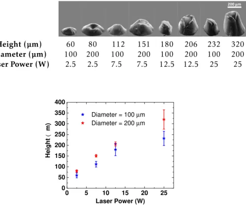
present results from molds fabricated using laser vetor mode on h-PDMS with circles, where one observes that the higher the laser power, the higher the microstructures are. In this specific study, a 45 % increase in laser power gives rise to structures with a height five times bigger.
Table 3.3: Summary of height measurements of semi-spheres using different
combina-tions of designed base diameters and laser powers.
200 µm
Height (µm) 60 80 112 151 180 206 232 320
Diameter (µm) 100 200 100 200 100 200 100 200
Laser Power (W) 2.5 2.5 7.5 7.5 12.5 12.5 25 25
0 5 10 15 20 25
0 50 100 150 200 250 300 350 400
Diameter = 100 µm Diameter = 200 µm
H e ig h t (m m )
Laser Power (W)
Figure 3.2: Semi-spheres height measured from SEM images versus laser power used to engrave the molds from where the resultant structures were peeled off. Values presented
correspond to average values ± standard deviation of a minimum of 15 measurements.
A relation between diameter and height is also observable, once the higher the de-signed diameter, the higher the semi-sphere height is. This results from the fact that engraving larger areas comprises deeper engraving on molds. Regarding these results, laser power of 2.5 W and 7.5 W showed up as being the most likely to produce semi-sphere like structures.
3 . 1 . PAT T E R N I N G
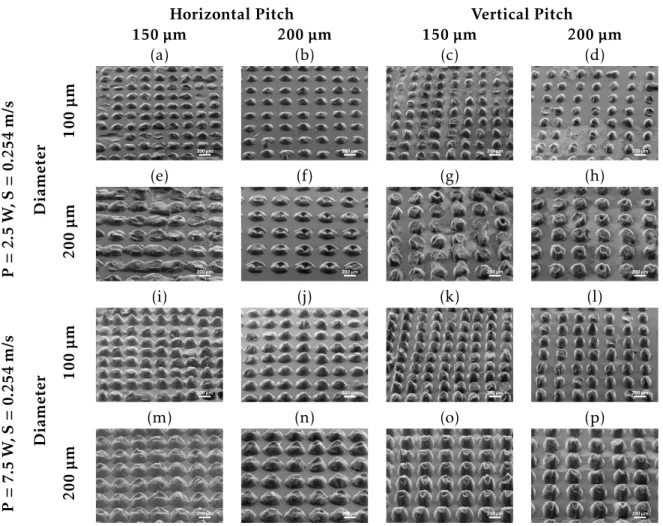
Furthermore, microstuctures resultant from two similar designs were used to compare the theoretical diameter and pitch with the resultant ones, as well as to compare the resolution over vertical and horizontal directions. The first design is based on circles with a theoretical diameter of 200 µm and a pitch of 150 µm, while the second design is based on circles with a theoretical diameter of 200 µm and a pitch of 200 µm. To do so, molds were made using a laser power of 2.5 W and 7.5 W, maintaining speed at 0.254 m/s for both. Table3.4shows the general view of the resultantPDMSstructures exhibiting nice homogeneity for each pattern, while highlighting the differences between pitches and
diameters over horizontal and vertical directions. From the images one notices that each feature can easily be discerned even for the lower pitch, meaning that theoretical pitch of about 150 µm is achievable with this technique.
Table 3.4: SEM images acquired of microstructured PDMS films. Images (a)-(h) result from molds engraved with a laser power of 2.5 W and 0.254 m/s laser speed for different
pitches and diameters. Images (i)-(p) result from molds engraved with a laser power of 7.5 W and 0.254 m/s laser speed for diferent pitches and diameters.
Horizontal Pitch Vertical Pitch
150 µm 200 µm 150 µm 200 µm
P = 2.5 W ,S = 0.254 m/s Diameter
(a) (b) (c) (d)
100
µm
200 µm 200 µm 200 µm 200 µm
(e) (f) (g) (h)
200
µm
200 µm 200 µm 200 µm 200 µm
P = 7.5 W ,S = 0.254 m/s Diameter
(i) (j) (k) (l)
100
µm
200 µm 200 µm 200 µm 200 µm
(m) (n) (o) (p)
200
µm
200 µm 200 µm 200 µm 200 µm
As previously seen, measurements over both horizontal and vertical directions should be performed in order to thoroughly analyse features. Hence, all semi-spheres were mea-sured over both directions of the engraving process. TableA.1summarizes the measured
C H A P T E R 3 . R E S U LT S A N D D I S C U S S I O N
diameter and pitch of the fabricated features, showing that although diameter and pitch values were usually far from what was designed, the sum of diameter and pitch tends to be very close to the expected sum of the designed ones. This can be explained by the fact that laser beam melts morePDMS than it was designed, performing engravings much larger than expected, which is corroborated by the discrepancy, sometimes larger than 100 µm, on measured diameters. Therefore, pitch for its turn, shows to be much smaller
100 150 200 250 300 350 100 150 200 250 300 350 R e a l D ia m e te r (m m )
Designed Diameter (m m)
Pitch = 150 m m
Horizontal Vertical
Pitch = 200 m m
Horizontal Vertical
y = x 2.5 W Laser Power
(a)
100 150 200 250 300 350 400 100 150 200 250 300 350 400 R e a l D ia m e te r (m m )
Designed Diameter (m m)
Pitch = 150 m m
Horizontal Vertical
Pitch = 200 m m
Horizontal Vertical
y = x 7.5 W Laser Power
(b)
Figure 3.3: Real diameter of PDMS semi-spheres, measured over horizontal and vertical directions of laser engraving versus designed diameter in Adobe Illustrator, produced with a laser power of (a) 2.5 W or (b) 7.5 W. The lines y = x illustrate a real diameter equal to the one designed. Values presented correspond to average values ± standard deviation of a minimum of 15 measurements.
0 50 100 150 200 250 0 50 100 150 200 250 R e a l P it c h (m m )
Designed Pitch (m m)
Diameter = 100 m m
Horizontal Vertical
Diameter = 200 m m
Horizontal Vertical
y = x
2.5 W Laser Power
(a)
0 50 100 150 200 250 0 50 100 150 200 250
Diameter = 100 m m
Horizontal Vertical
Diameter = 200 m m
Horizontal Vertical
y = x
R e a l P it c h (m m )
Designed Pitch (m m)
7.5 W Laser Power
(b)
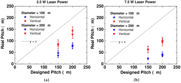
Figure 3.4: Real pitch between PDMS semi-spheres, measured over horizontal and vertical directions of laser engraving versus designed pitch in Adobe Illustrator, produced with a laser power of (a) 2.5 W or (b) 7.5 W. The lines y = x illustrate a real pitch equal to the one designed. Values presented correspond to average values ± standard deviation of a minimum of 15 measurements.
3 . 1 . PAT T E R N I N G
than expected to maintain the design. Laser engraving resolution in vertical direction is notably better than in horizontal direction once features measured in vertical direction of the laser engraving show values of diameter and pitch closer to the designed ones, as it is shown on Figure3.3and Figure3.4, respectively.
As a result of all the explained before, the molds chosen for fabrication of PDMS
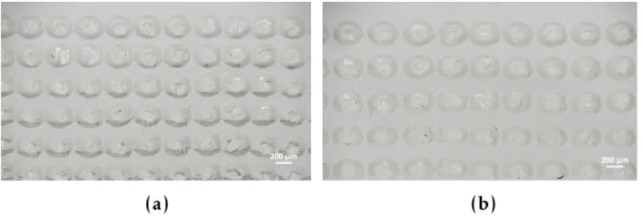
membranes come as a combination of using designs with circles to be engraved on h-PDMSwith a laser engraving machine on vector mode. The parameters chosen were 7.5 W of laser power and speed of 0.254 m/s, as with this combination more reproducible semi-sphere structures are achivable. Two molds using this combination of parameters were produced, both with theoretical diameters of 200 µm – the first with a pitch of 150 µm and the second with a pitch of 200 µm. Figure 3.5shows the two molds produced and Figure3.6shows a microscope image of eachPDMSmold that was used to fabricate membranes present in the studies further explained in this work, which were measured to have a thickness of 215 µm ± 19 µm (average values ± standard deviation) corresponding to a minimum of 15 measurements.
Figure 3.5: Molds produced for fabrication of membranes. Mold on the left designed with circles with 200 µm of diameter and pitch = 150 µm. Mold on the right designed with circles with 200 µm of diameter and pitch = 200 µm
200 µm
(a)
200 µm
(b)
Figure 3.6: Microscope acquired images of the fabricated molds. (a) Mold designed with diameter = 200 µm and pitch = 150 µm. (b) Mold designed with diameter = 200 µm and pitch = 200 µm.
C H A P T E R 3 . R E S U LT S A N D D I S C U S S I O N
3.2 Ink Study
3.2.1 Carbon-ink dilution study
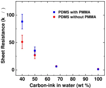
Studies over carbon-ink dilutions and number of layers were performed to further explore the best conductive film to fabricate piezoresistive sensors. Herein,PMMAwas investi-gated as a coating layer between carbon-ink andPDMSto check if it could both improve the adhesion of carbon ink toPDMSand the final stability of the device. Firstly, to investi-gate the possibility of using less carbon-ink without compromising the good functionality of the piezoresistive sensors, sheet resistance of smooth carbon-coatedPDMSand smooth carbon-coatedPDMSwithPMMAwas measured by varying the dilution of the coating in water (100 wt %, 67 wt %, 50 wt %, 40 wt %). Figure3.7shows a comparison of sheet resistance between carbon-ink deposited onPDMSwith and withoutPMMA. Both curves tend to decrease in sheet resistance as carbon-ink concentration in water increases, as expected. From this study it was found that sheet resistance for 50 wt % and 40 wt % dilutions, for bothPDMSwith and withoutPMMA, is excessively high for a conductive film, with average resistance values above 30 kΩ/. For films with approximately 67 wt
40 50 60 70 80 90 100
0 50
100 PDMS with PMMAPDMS without PMMA
S h e e t R e s is ta n c e ( k W/ÿ )
Carbon-ink in water (wt %)
Figure 3.7: Sheet resistance of smooth carbon-coated PMDS and PMMA-coated PDMS for four different carbon-ink dilutions in water. Measurements presented here correspond to
average values ± average absolute deviation of a minimum of 3 measurements.
% dilution, the sheet resistance is (6.7 ± 1.2) kΩ/and (6.4 ± 0.8) kΩ/, respectively for smooth carbon-coatedPDMSand smooth carbon-coatedPDMSwithPMMA.
Using a concentration of 100 wt % of carbon-ink ensures a sheet resistance of about (1.3 ± 0.1) kΩ/and (1.6 ± 0.3) kΩ/, respectively forPDMSwith and withoutPMMA, which is suitable for the fabrication of piezoresistive pressure sensors. Figure3.7 illus-trates that 67 wt% and 100 wt% dilutions allow an easy replication of the membranes produced as the sheet resistance average values are deviated by a small error.
3 . 2 . I N K S T U DY
3.2.2 Ink layers study
To further understanding the relation between carbon coating layers and their behaviour on the device, a study comparing sheet resistance of different deposited layers using the
dilutions of 67 wt% and 100 wt% was accomplished. Figure 3.8ashows a comparison of sheet resistance as a function of the number of layers forPDMS andPMMA-coated
PDMS.
Regarding the 67 wt% dilution of carbon-ink onPDMSwithPMMA, sheet resistance of one layer is approximately (6.4 ± 0.8) kΩ/. Sheet resistance, as expected, decreases with the number of carbon layers deposited by spin-coating as the amount of conductive coating increases. The deviation error also decreases which means that the conduction mechanism is becoming homogenous for the whole membrane. Both dilutions tend to a limit of sheet resistance with the increasing layers. Nevertheless, as expected, the 67 wt% dilution requires more stacked layers to reach the same values of sheet resistance of 100 wt%. Therefore, for 100 wt% dilution, there was no need to perform studies over more layers, once the values were already low enough. The sheet resistance onPDMSvalues are close to the ones with the same dilution onPMMAfor both dilutions studied here, however, it appears to have higher deviation error, which meansPMMAonPDMSseems to contribute for a greater stability of carbon coating adhesion.
The first carbon coating layer for all four curves shows a larger deviation error of sheet resistance than for all other layer depositions due to the heterogeneity of deposited carbon. This observation is corroborated by the deviation errors for thickness, which were also measured in this study.
1 2 3 4 5
0 2 4 6 8
Number of carbon coating layers
67 wt% w/PMMA 67 wt% 100 wt% w/PMMA 100 wt% S h e e t R e s is ta n c e ( k W / ÿ ) (a)
1 2 3 4 5
0 4 8 12 16 20 24 28 T h ic k n e s s ( m m )
Number of carbon coating layers
67 wt% w/PMMA 67 wt% 100 wt% w/PMMA 100 wt%
(b)
Figure 3.8: (a) Sheet resistance of 67 wt% and 100 wt% carbon coating dilutions in water on smooth PDMS films and PMMA-coated PDMS films with 1 to 5 layers of coating. (b) Thickness of 67 wt% and 100 wt% carbon coating on smooth PDMS films and PMMA-coated PDMS films with 1 to 5 layers of coating. Measurements presented here correspond to average values ± average absolute deviation of a minimum of 3 measurements.
Thicknesses presented on Figure3.8bwere measured between the top of the coating
C H A P T E R 3 . R E S U LT S A N D D I S C U S S I O N
layers and the top of PDMS membranes, meaning that the presented thickness corre-sponds to the sum of every layer onPDMS, includingPMMA, if applicable. This figure highlights a more linear behaviour for thickness in function of layer depositions onPMMA
for both dilutions than for deposited layers onPDMS, which confirms thatPMMAplays an important role on carbon coating adhesion.
Given that the purpose of this work is to produce thin and flexible membranes, a trade-offbetween thickness and resistance has to be reached. Although membranes coated with
100 wt% carbon coating show higher thickness, they also show relatively lower resistance when compared with membranes coated with 67 wt% carbon coating. Therefore, 100 wt% carbon coating dilution with only one coating layer was chosen over other dilutions once it presents a very reasonable value of sheet resistance and comprises the lowest thickness possible with this sheet resistance value.
3.2.3 Electrical Characterization of carbon-coated membranes
Moreover, microstructured membranes using the chosen carbon coating dilution were also electrically characterized to investigate the role of microstructures on membrane re-sistance. FigureB.1ashows results for four different membranes containing semi-spheres
with a diameter of 200 µm and a pitch of 150 µm, whereas FigureB.1bresults from the study for four different membranes with semi-spheres with a diameter of 200 µm and
a pitch of 200 µm. Both figures prove the ohmic behaviour of carbon coating on mem-branes and therefore the same ohmic behaviour was expected for the whole device when current flows from a membrane to the other. Both figures allow the estimation of the average nominal resistance for each membrane pattern which is calculated to be (1.2 ± 0.4) kΩ/and (1.2 ± 0.2) kΩ/for microstructures with the lower pitch and the higher pitch, respectively.
3.2.4 Morphological Characterization of carbon-coated membranes
Microstructured carbon-coated membranes were also morphologically characterized us-ingSEM, in order to analyse membrane’s thickness, semi-spheres’ diameter, pitch, and height as well as the homogeneity of carbon coating. Figure 3.5a to Figure3.5d show a general view of the produced 200 µm diameter semi-spheres. All images show the engraving direction over the vertical direction as it becomes easier to contrast the pitch. Figure3.5c and Figure3.5d present semi-spheres with greater height due to the presence ofPMMAon their structure, which can also be corroborated by measurements acquired of the dimensions of the microstructures present in SectionC.
Overall, all images acquired show homogeneity over all structures, with semi-spheres perfectly aligned over both vertical and horizontal directions. When facing two mem-branes to produce a piezoresistive device, the pitch and diameters chosen for these pat-terns will promote the contact between both groups of semi-spheres, hence granting reproducibility over devices and possibly contributing for a lower nominal resistance due
3 . 2 . I N K S T U DY
Table 3.5: SEM images of microstructures produced on PDMS with carbon and PMMA + carbon coatings. Images (a)-(d) general view of aligned semi-spheres with a designed base diameter of 200 µm, with pitches of 150 µm - (a),(c) or 200 µm - (b)(d). Images (e)-(h) close up view of aligned semi-spheres with a designed base diameter of 200 µm, with pitches of 150 µm - (e),(g) or 200 µm - (f),(h).
Pitch
150 µm 200 µm
G
ener
al
V
iew
C
arbon
(a) (b)
200 µm 200 µm
P
MMA
+
C
arbon
(c) (d)
200 µm 200 µm
Cl
ose
up
V
iew
C
arbon
(e) (f)
40 µm 40 µm
P
MMA
+
C
arbon
(g) (h)
40 µm 40 µm
C H A P T E R 3 . R E S U LT S A N D D I S C U S S I O N
to more contact spots for electrical current flowing. Figure3.5e to Figure3.5h show that both layers,PMMAand carbon coating, seem to spread homogeneously overPDMS sur-face and semi-spheres, once semi-sphere structures are not sharp enough to avoid coating to adhere there as well as it adheres in other substrate spots.
3.3 Homemade Pressure Applying System
Testing the fabricated devices comprises measuring the device’s piezoresistive signal in response to an applied pressure and comparing fabricated devices requires the applica-tion of the same pressure on every single sample. Therefore, and to overcome the lack of systems applying a reproducible force, a homemade system with this purpose was built. In Figure 3.9, a simplified block diagram illustrates the system principal components and functions, consisting in an Arduino to control the entire system, a stepper motor driver, aliquid crystal display (LCD)display to act as user interface (allowing to define frequency and pressure for measurements as well as to set the tip on the desired spot), and the stepper motor Motor Nema17.
Arduino
Driver Stepper Motor
LCD Display
Figure 3.9: Block diagram representing the blocks constituting the system built - an arduino controlling the stepper motor driver and the LDC display.
Figure3.10 shows the built circuit used for the developed system. Figure3.11 rep-resents the developed system, from where one can clearly realize each component and from where one may see that the critical element of the apparatus is the conversion of radial force in vertical force and what enables this is the motor which, once in movement, makes the arm connected to it to move vertically, applying a force that is directly propor-tional to the displacement of the tip of the arm. This system, among other components, is provided with a piezoelectric sensor (piezoelectric coefficient, d33= 800 pC/N and a
capacity, C = 20 nF) capable of detecting a response signal which can be then converted to force (N), allowing a continuous monitoring of the applied pressure on the fabricated devices. The tip of the system, element which is in contact with devices, consists in a rubber, mechanically characterized with a Young’s Modulus of 15 MPa.
The black-painted components present in Figure3.11were designed in the 3D mod-eling computer program SketchUp, as seen in SectionDand subsequently printed in a 3D printer Prusa i3. The acrylic components were cut in the laser engraving machine in designs previously drawn in Adobe Illustrator (2015.0.0). The section of the code
3 . 3 . H O M E M A D E P R E S S U R E A P P LY I N G S YS T E M
Figure 3.10: Circuit design for the development of the system. The circuit consists in an Arduino board controlling a stepper motor driver and a LCD. A 9 V voltage is the source of the system, used to power the motor and to power Arduino after being converted to 5 V by a 7805 voltage regulator. A potentiometer is also connected to the arduino to help in user interface.
responsible for the movement of the stepper motor and therefore, the movement of the tip, is also presented in SectionDas well as a schematic of the whole developed system with indication of each component. Moreover, in order to have a clear signal from the piezoelectric sensor, a RC Low-Pass Filter with Op Amp Buffer with 3 poles represented
in SectionD, was connected to the system.
In the conformation exhibited in Figure3.11, this homemade system is able to provide pressures applied in frequencies from 0.5 Hz to 20 Hz with electrical signals from both piezoelectric sensor and piezoresistive fabricated devices simultaneously monitored and recorded on an oscilloscope. The range of pressure being applied by the machine can be adjusted depending on what is the final object applying the force, meaning that, using materials with larger area than the rubber, one can reach lower pressures. Figure 3.12
shows the output signal of the piezoelectric device, responding to stimulus performed by the machine in order to ascertain the limits of the system mounted as previously shown. Figure 3.12arepresents the sinusoidal pressure being applied on the piezoelectric sen-sor by a vertical displacement of the rubber on the sensen-sor of 70 µm, with the maximum frequency possible for the apparatus. This displacement results in a maximum applied pressure of approximatelly 130 kPa. Figure3.12brepresents the same displacement but with lower frequency and applying a maximum pressure of approximatelly 600 kPa. The change of wave type to an approximately square wave can be explained by the fact that the motor to perform a displacement of 70 µm, only rotates 1 step and at low frequencies
C H A P T E R 3 . R E S U LT S A N D D I S C U S S I O N
Figure 3.11: Picture representing the pressure apllying system developed.
1 step seems to be insufficient for this time interval and therefore motor stays immobile
for most of the time. Figure3.12crepresents a vertical displacement of 700 µm with a fre-quency of 20 Hz, corresponding to an applied pressure of approximately 1.4 MPa, which consists in an increase in pressure of about 10 times when compared to a displacement 10 times lower with the same frequency. Although the values seem very conformal with the expected, the stepper motor finds dificult succeding in performing the desired frequency as this seems to be a very high displacement for the frequency of 20 Hz, as seen in the plot. Figure 3.12dalso results from a vertical displacement of 700 µm but with a frequency of 0.5 Hz. The maximum pressure applied for this displacement is 5.1 MPa, consisting in a increase of pressure of about 9 times when compared with a displacement 10 times lower with the same frequency. From theses results, it was proven the good behaviour of the system on the frequencies tested. The results also showed that the minimum pres-sure applied for this conformation was approximately 130 kPa and the maximum was approximately 5.1 MPa.
3 . 4 . E L E C T R I CA L C H A R AC T E R I Z AT I O N O F D E V I C E S
0.00 0.02 0.04 0.06 0.08 0.10 0 20 40 60 80 100 120 140 160 Time (s) P re s s u re ( k P A )
d = 70 m m, f = 20 Hz
(a)
0 1 2 3 4 5
0 200 400 600 800 1000 Time (s) P re s s u re ( k P A )
d = 70 m m, f = 0.5 Hz
(b)
0.00 0.02 0.04 0.06 0.08 0.10 0.0 0.5 1.0 1.5 2.0 Time (s) P re s s u re ( k P A )
d = 700 m m, f = 20 Hz
(c)
0 1 2 3 4
0 1 2 3 4 5 6 Time (s) P re s s u re ( k P A )
d = 700 m m, f = 0.5 Hz
(d)
Figure 3.12: Pressure applied on piezoelectric sensor versus time. (a) Displacement of 70 µm and frequency of 20 Hz. (b) Displacement of 70 µm and frequency of 0.5 Hz. (c) Displacement of 700 µm and frequency of 20 Hz. (d) Displacement of 700 µm and frequency of 0.5 Hz.
3.4 Electrical Characterization of Devices
The fabricated devices were submitted to tests over sensitivity, nominal resistance and ohmic-like contact. First of all, sealing two membranes with the microstructure domain facing each other is a dominant factor in device fabrication, because the contact between two opposite semi-spheres caused by an external loading is what generates a change in the electrical resistance signal. Consequently, for a good reproducibility of devices, mem-branes require to be similarly sealed. Tests on sealing memmem-branes with and without a window of Kapton tape acting as a spacer between the membranes were also performed, showing no evidence of improvements in using the tape as devices’ sensibility is not influ-enced by it. Tests on I-V curves of the fabricated devices were conducted, exhibiting sheet resistance of approximately 1 kΩ/proving the good tendecy of devices to ohmically conduct current from one membrane to the other, as shown on Figure3.13.