Application Note AN-1044
revA
IPM
Application Overview
Integrated Power Module for Appliance Motor Drives
By P. Wood, M. Battello, N. Keskar, A. Guerra
Table of Contents
Page
Introduction ...1
IPM
Solution...
...
...3
IPM System Description
.
...
...3
Internal Circuitry ...
...
...3
Input Signals ...3
IRAMS10UP60A Pin Description ...4
Bootstrap Circuit Operation ...4
Operation of the Circuit ...4
Bootstrap Diode ...5
Low Modulation Frequency Operation ...5
Power Loss Estimation...7
Thermal Resistance in Module...8
Thermal Design (heat sink selection) ...10
Thermal Diagram ...10
Design Example ...10
Packaging and Installation Guide...11
The System Schematic ...12
Bus Capacitor Calculation ...13
Controlling Capacitor Over-Voltage...13
Auxiliary Power Supply ...14
Power Analysis...15
The IR Solution ...15
Buck Converter Design ...15
The Regulator Control Loop ...16
Inductor Calculation ...16
General Low-Current Sensing...18
Problem Analysis ...18
Solution ...18
Typical Example Circuits ...18
These modules represent a sophisticated, integrated solution for 3 phase motor drives used in a
variety of appliances, such as washing machines, energy efficient refrigerators and air
AN-1044
Introduction
These modules represent a sophisticated, integrated solution for 3 phase motor drives used in a variety of appliances, such as washing machines, energy efficient refrigerators and air conditioning compressor drives in the 250 Watt to 2 Kilowatt power range. They utilize NPT(non-punch through) IGBTs matched with Ultra-soft recovery diodes to minimize EMI generation. In addition to the IGBT power switches, the modules contain a 6 output monolithic driver chip, matched to the IGBTs to generate the most efficient power switch consistent with minimum noise generation and maximum ruggedness.
• Packaging options include staggered pinout for maximum creepage distances and straight or 90° bend options for heat-sinks parallel or perpendicular to the circuit board.
• Capacitive switch noise coupling to the mounting surface is prevented by a ground plane isolated to 2000Vrms connected to the Vss pin.
• Insulated Metal Substrate technology ensures low thermal resistance and less stringent flatness require-ments for the heat-sink. It also offers significant flexibility in the module layout and internal electrical system.
Application Note
IPM Application Overview
Integrated Power Module for Appliance Motor Drive
AN-1044
23 VS1
24 HO1
25 VB1
1 VCC
2 HI N1
3 HI N2
4 HI N3
5 LI N1 LI N2
6 LI N3
7 F 8
I TRI P 9
EN 10
RCI N 11
VSS 12
COM 13 22
VB2 21 HO2
20 VS2
19 VB3
18 HO3
17 VS3
VRU (12)
VRW (14) VRV (13)
VB1 (7) U, VS1 (8)
VB2 (4) V, VS2 (5) VB3 (1) W, VS3 (2)
THERMI STOR R3
VDD (22)
VSS (23)
R1
R2
C
Rg1 Rg3 Rg5
Driver I C
RT
LO1 16
LO3 14 LO2 15
Rg2
Rg4
Rg6
T/ ITRI P (21) HI N1 (15) HI N2 (16) HI N3 (17)
AN-1044
IPM
Solution
Apart from the better known advantages of mod-ules (smaller, more reliable, single component) compared with discrete solutions, the IPM modules
re-lieve the designer from several pitfalls often associated with IGBT inverter designs:
• Lower circuit inductance than discrete solutions results in voltage spike reduction and the ability to operate at higher switching frequency with lower switch losses.
• Simple power connection, just V+, the emitter connections Le1, Le2 and Le3 and the motor connections U,V and W.
• The integrated driver requires only 6 logic level inputs. (includes 3.3V logic) and 3 bootstrap ca-pacitors selected for the switching frequency. • Propagation delays for all low-side and high-side
IGBTs are matched to prevent DC core flux from being applied to the motor.
• Built in dead time control prevents conduction overlap between high-side and low-side IGBTs. • Fail-safe operation is ensured by built in shut down features for over current and over tempera-ture.
• Analog temperature monitor and phase leg cur-rent pins are provided.
IPM
System Description
The primary advantage in using the IPM modules is the ease in which an optimized, reliable motor drive system can be implemented. The designer is relieved of the followingheadaches:
• How to provide sufficient dead time to prevent shoot through failures.
• How to design an overcurrent protection circuit to protect the IGBT switches.
• How to design an over-temperature detection circuit that actually monitors IGBT temperature. • How to match propagation delay times in the drive circuits to prevent DC current flow in the motor windings.
• How to select the optimum switch times to mini-mize EMI generation and maximini-mize efficiency. • How to minimize inductive loop size for minimum
turn-off voltage overshoots in the IGBTs. The IRAMS module provides answers to all the above questions in a compact, electrically isolated package.
Internal circuitry
The 600V IRAMS module contains six IGBT die each with its own discrete gate resistor, six commutation diode die, one three phase monolithic, level shifting driver chip, three bootstrap diodes with current limiting resistor and an NTC ther-mistor/resistor pair for over temperature trip. The over current trip circuit responds to an input voltage generated from an ex-ternal sense element such as a current transformer or sense resistor. The input pin for the trip circuit performs a dual func-tion:
• Input pin for over current trip voltage.
• Output pin for module analog temperature sensing thermistor.
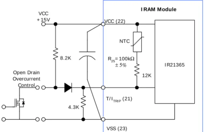
Because of the dual function requirements, an external circuit similar to the diagram below is recommended.
It is important that the Vcc filter capacitor is connected directly at the IRAMS module to prevent noise from propagat-ing into the Itrip circuit to cause false tripppropagat-ing. The open col-lector, over current control transistor is normally ‘on’ and in-hibits the over current function. The over temperature circuit is always active and is over-ridden by the current circuit in the event of over current detection.
Figure 1: Over current interface circuit
Input signals
The complete, open loop motor drive system com-prises a signal source, a drive stage and a power stage. The three phase motor can be a simple induction type, or a perma-nent magnet synchronous type. The IRAMS module integrates the driver and power stages into an isolated module but the ‘brains’ of the system must generate timing, speed and direc-tion PWM or PFM informadirec-tion to complete the motor drive func-tion.
5 volt logic systems are generally preferred from a noise
VCC (22)
T/ ITRI P ( 21)
NTC
12K
VSS (23) 4.3K
I R21365
I RAM Module
8.2K VCC + 15V
R25= 100kΩ ± 5%
AN-1044
immunity standpoint but the module can also accept 3.3V logic or any pulse input up to the Vcc level (+15V).
The monolithic driver IC inputs require a logic low to command an output. The Itrip input is 4.3V nominal and the under voltage lockout voltage is 11V. Further information on IR21365 characteristics is available at www.irf.com .
I
RAMS10UP60A Pin Description
Figure 2: Power module PIN out.
Pin 1: VB3 Bootstrap capacitor Phase W.
2: VS3 Phase W output (high-side emitter
Phase W)
3: Position empty for creepage
voltage.
4: VB2 Bootstrap capacitor Phase V.
5: VS2 Phase V output (high-side emitter
Phase V)
6: Position empty for creepage
voltage.
7: VB1 Bootstrap capacitor Phase U.
8: VS1 Phase U output (high-side emitter
Phase U)
9: Position empty for creepage
voltage.
10:V+ Positive bus voltage.
11: Position empty for creepage
voltage.
12:Le1 Low-side emitter Phase U.
13: Le2 Low-side emitter Phase V.
14: Le3 Low-side emitter Phase W.
15: HIN1 High-side input Phase U.
16: HIN2 High-side input Phase V.
17: HIN3 High-side input Phase W.
18: LIN1 Low-side input Phase U.
19: LIN2 Low-side input Phase V.
20: LIN3 Low-side input Phase W.
21: ITRIP Over current and tempera
ture shut-down.
22: VCC +15V bias voltage.
23: VSS 15V return and substrate
ground plane.
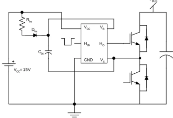
Bootstrap Circuit Operation.
The high and low-side driver IC requires a float-ing voltage supply for each of the three high-side cir-cuits that provide gate pulses to high-side IGBTs. A very convenient way of obtaining such floating voltage sup-plies is usage of bootstrap circuits. The following figure shows such an implementation for one phase of a three-phase switching inverter drive. The circuit is repeated for each phase.
Figure 3: Schematic showing bootstrap circuit for one phase
Operation of the circuit is as follows
When the low-side IGBT is on, the bootstrap capacitor Cbs charges through the bootstrap diode Dbs, resistor Rbs and low side switch S2 to almost 15 V, since the Vs pin of the IC is almost at ground potential. The capacitor Cbs is so designed that it retains most of the charge when the low-side device switches off and the Vs pin goes to almost the bus potential. Then, the voltage Vbs being almost 15 V, the high-side circuit of the driver IC is biased by the capacitor Cbs. Selection of the bootstrap capacitor, diode and resistor is gov-erned by several factors:
1. Voltage Vbs has to be maintained at a value higher than the under-voltage lockout level for the IC driver.
2. The capacitor Cbs does not charge exactly to 15V when the low-side switch is turned on, depending upon the drop across the bootstrap diode (Vfbs) and low-side switch (VceonS2).
3. When the high side switch is on, the capacitor discharges mainly via the following mechanisms: a. Gate charge Qg for turning the high-side switch
on
b. Quiescent current Iqbs to the high-side circuit in the IC
VCC VB
HO
VS
HIN
GND Rbs
Dbs
Cbs
VBUS
AN-1044
c. Level-shift charge Qls required by level-shifters in the IC
d. Leakage current Idl in the bootstrap diode Dbs e. Capacitor leakage current Icbs (ignored for
non-electrolytic capacitors)
f. Bootstrap diode reverse recovery charge Qrrbs
Charge lost by the bootstrap capacitor in one switching cycle is given by the following equation:
SW SW f I Q f I Q Q Q DL LS QBS RRBS G
BS= + + + +
∆ (1)
where fsw is the switching frequency and the other param-eters are as defined earlier. This charge loss in the boot-strap capacitor as given above results in a drop in the volt-age Vbs across it. The value of Cbs can be designed based on the desired voltage drop in Vbs as follows,
BS BS BS V Q C ∆ ∆ = (2)
The drop in Vbs can be set as a percentage of the value of Vbs before turn-on of the high side switch. The lowest value of Vbs in one modulation cycle is given by
VBS=VCC−VFBS−VCEON(S2) (3)
Note that the above equation gives the worst-case value of the bootstrap voltage with the low side IGBT conducting cur-rent in conjunction with high side diode. Curcur-rent reversal leads to low side diode conduction in conjunction with the high side IGBT, whereupon the equation (3) changes to:
VBS=VCC−VFBS+VF(D2) (3a)
Combining equations (1), (2) and (3) and using ∆Vbs = 1 % of Vbs, we get:
) .(
01 .
0 CC FBS CEON(S2)
DL LS QBS RRBS G BS V V V f I Q f I Q Q
C SW SW
− − + + + +
= (4)
A series resistor Rbs is recommended as shown in figure 3. This limits peak currents in the bootstrap circuit during initial charging. These currents, if excessive, have been known to cause driver latch-up under fast switching conditions. Typically, the low side switch is switched with a constant duty-cycle for charging the bootstrap capacitor ini-tially. The time required for the initial bootstrap capacitor charging, after which input signals can be transferred to the switch gates, is given by:
− − − ≥ ) 2 ( (min) . . S CEON FBS BS CC CC BS BS V V V V V Ln D R C t (5)
In the above equation, D is the duty cycle of the charging pulses. Note that this discounts effects of discharging
pro-cesses and hence gives a minimum charging time.
BOOTSTRAP DIODE
When high side switch or diode conducts, the boot-strap diode supports the entire bus voltage. Hence for a 300-400 V system, Dbs has to be rated at 600 V. The peak current seen by Dbs is determined by the series resistor Rbs. However since this current spike is quite narrow, it does not seriously affect diode selection. Average current handled by the bootstrap diode is given by the product of the charge supplied to Cbs during every switching cycle expressed by equation (1) and the switching frequency fsw. In order to minimize the power loss in the diode and to reduce the size of the bootstrap capacitor, reverse recovery charge in Dbs should be as low as possible. For the same reason, reverse leakage current should also be low at the highest operating temperature. Finally, the knee voltage of the diode should be low to minimize the voltage drop across it during charg-ing.
LOW MODULATION FREQUENCY OPERATION
As was seen from equations (3) and (3a), the volt-age across the low side device (IGBT or diode) reverses polarity with direction of current flow. Hence the voltage ap-plied across the bootstrap circuit also varies accordingly, decreasing below Vcc when the low side IGBT conducts and increasing beyond Vcc when the low side diode con-ducts. This variation can be approximated for analysis to be sinusoidal in nature. For a sine current application the as-sumption is quite valid, since for practical current values, the voltage drop across the IGBT or diode varies almost linearly with current, except at very small current values. Then the voltage applied across the bootstrap circuit can be represented by:
V=VCC−VPKIsinωt (6)
when the low side IGBT is conducting with VpkI represent-ing peak voltage across the IGBT. Similarly, when the low side diode conducts, the equation above becomes:
V=VCC+VPKDsinωt (7)
AN-1044
Figure 4: Schematic showing effect of low side switch/diode conduction
The above schematic represents the situation for a single phase of the three-phase inverter. This is briefly analyzed below:
When the modulation frequency is lower than the cutoff fre-quency for the bootstrap circuit defined by the resistor Rbs, bootstrap diode voltage drop Vfbs and the capacitor Cbs, the capacitor voltage varies with time at the modulation fre-quency. When the low side IGBT is conducting, applied volt-age across the bootstrap circuit reduces sinusoidally, which means that the voltage across the sine voltage source in figure 4 is positive and increasing. Starting from the initial capacitor voltage of approximately Vcc, the bootstrap diode is reverse biased while the voltage V is rising from zero to VpkI. During each switching cycle, the voltage V changes by small value from the previous switching cycle by:
(
)
[
t Tsw t]
V
V= PKIsinω + −sinω
∆ (8)
where Tsw is the switching period. In this time, the capacitor discharges because of Iqbs and Idl only, since the high side IGBT is not switching. There is no charging of the bootstrap capacitor, the diode Dbs being reverse biased. Capacitor voltage therefore decreases approximately in a linear fash-ion. As the voltage V crosses VpkI, the capacitor voltage is already at a steady value given by the difference between Vcc and VpkI. After this, the voltage V decreases sinusoi-dally and the capacitor voltage follows the sine wave till the voltage V reaches zero. During this quarter cycle from VpkI to zero, the diode Dbs is forward biased enabling bootstrap capacitor charging. The charge supplied per cycle is then equal to the charge lost in the quiescent currents plus the charge required to raise the capacitor voltage by the change in V in one switching cycle, which is:
(
)
[
t Tsw t]
V
V= PKIsinω + −sinω
∆ (9)
Thus the charge supplied per switching cycle is:
(
)
[
]
SW f I I t Tsw t CVQ= PKI + − + QBS+ DL
∆ sinω sinω + Q
RRBS (10)
The term in brackets is approximately equal to the product of first differential of sin ωt with respect to t, and the switch-ing time Tsw. This has a maximum value of ωTsw. Then the worst-case average current through the bootstrap circuit
dur-ing the quarter cycle under consideration is:
SW SW f Q f I I Tsw CV
IAVG PKI QBS DL RRBS
+ + +
= ω (11)
When the voltage V crosses zero and becomes negative, the above analysis still applies with the additional charge required for switching the high side device. Then the worst-case average current in the bootstrap circuit is:
SW SW f Q Q Q f I I Tsw CV
I G LC RRBS
DL QBS PKD AVG + + + + + = ω (12)
This continues for one quarter-cycle before the voltage V reaches Vpkd. After V crosses Vpkd and starts increasing to zero, the bootstrap diode is reverse biased and the ca-pacitor discharges every cycle without a refresh charge. Hence the voltage across the capacitor goes on decreas-ing. Since the resistor Rbs carries bootstrap currents for all three phases, the worst case current for one quarter of the modulation period at a stretch (neglecting the 120 ° phase difference) is three times the value given in equation (12).
It is seen from equation (12) that the first term is independent of the switching frequency and depends upon the voltage drop across the low-side devices, the value of the bootstrap capacitor and the angular frequency corre-sponding to the sinusoidal modulation. The rest of the ex-pression is the product of the refresh charge calculated in equation (1) and the switching frequency. This part is inde-pendent of the modulation frequency.
The IR module IRAMS10UP60 contains three boot-strap diodes and a series resistor connected internally be-tween the 15 V supply Vcc and individual Vb pins of the three phases. Hence only appropriate bootstrap capacitors need be connected on the external board. Some layout as-pects have to be considered before doing that. Bootstrap capacitors should be connected as close to the Vb and Vs pins as possible to reduce stray inductance in the connec-tions. Furthermore, it is recommended to use a small high frequency capacitor in parallel to a larger low frequency bootstrap capacitor.
It can be shown that the power loss in the series resistor selected is well within limits. From equation (12), substituting under worst conditions:
C = 10µF, Vpk = 2.5V,ω = 2πx 100rad/s, fsw = 20kHz, Iqbs = 150µA, Idl = 5µA, Qg = 40nC, Qlc = 5nC, Qrrbs = 25nC, we get IAVG = 17.3 mA.
Then average resistor current = 50 mA
Using IRMS = 1.5 IAVG, IRMS = 75 mA. This gives the resistor power loss 11.25 mW.
Rbs Dbs
Cbs
VCC
VI GBT/ VD
AN-1044
POWER LOSS ESTIMATION
The IRAMS modules use 600 V non-punch-through (NPT) IGBTs with a 10 µs short-circuit capability, that are well optimized for switching and conduction losses. Hyperfast diodes with very low reverse recovery charge and reduced forward drop at high temperatures further improve the turn-on performance of the IGBTs. As the cturn-onductiturn-on losses are approximately constant with switching frequency for a given current and bus voltage levels, appropriate trade-off has to be obtained in selecting the switching frequency best suited for a particular device.
There have been many attempts to estimate switch-ing energy values at turn-on and turn-off based on semi-conductor device models. However the complexity associ-ated with making such models accurate suggests that a more pragmatic approach would be measuring elemental energy losses and calculating total power losses using system level models. Switching losses for IGBT and diode can be mea-sured and modeled empirically as functions of voltage, cur-rent and temperature. Similarly on-state voltage drop can be represented as a function of current and temperature.
(
)
(
)
b T CEON
n y OFF
k x ON
aI V V
I I m m E
I I h h E
+ =
+ =
+ =
. 2 1
. 2 1
(13)
In the above equations, VT is the voltage drop across the IGBT/diode at zero current and h1, h2, x, k, m1, m2, y and n are empirical parameters obtained to get a good curve-fit between measured and calculated values. Then knowing the current variation with time and knowing the switching frequency, each of the above losses can be cal-culated either as a function of time or as an average over
one period of current either using a spreadsheet or from closed-form solutions. Power losses so calculated can then be used to estimate temperatures of components inside the module, using specified thermal resistance numbers.
EXAMPLE
For a 1 HP (@ max. voltage) induction motor, sup-plied from an inverter with a DC bus of 400 V, the maximum RMS motor voltage would be about 226 V line to line with a modulation index of 0.8. Then the inverter output current per phase is about 3.2 A RMS (4.53 A peak) with a power factor of 0.6. This current can be expressed approximately as:
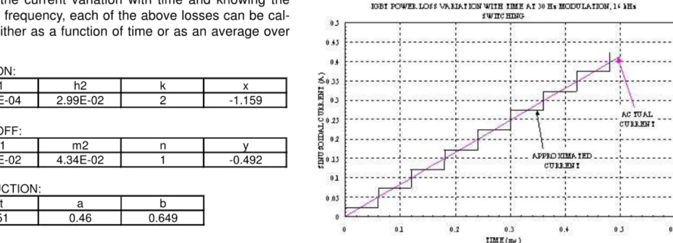
I = 4.53 sin(ωt) (14)
The loss parameters for the IGBT under question are as given in the Table 1. Knowing the switching frequency, the energy losses can be averaged per switching cycle giving power loss per switch cycle. For purposes of calculation, the current can be approximated to be constant for one switching period. This is shown in the figure 5. Assuming that the current varies linearly within one switching cycle and the variation is small, the average current in the switch-ing cycle can be assumed to be constant throughout the switching period. The value of the average current then var-ies sinusoidally between switching cycles as given in equa-tion 14. The switching energies at turn-on and turn-off, and the conduction drop can be calculated for each switching cycle using equations 13 and 14. For each switching cycle, the average power loss including switching and conduction power loss, can be calculated giving a time-variant power loss as shown in figure 6. This figure shows power loss varia-tion for half a modulavaria-tion cycle i.e. for one IGBT. Knowing this, the average power loss can be easily calculated per IGBT and for a 3-phase inverter system.
TURN-ON:
h1 h2 k x
7.69E-04 2.99E-02 2 -1.159
TURN-OFF:
m1 m2 n y
1.76E-02 4.34E-02 1 -0.492
CONDUCTION:
Vt a b
0.51 0.46 0.649
Table 1. Power loss estimation parameter for IGBT in example Figure 5: Plot showing approximation of sine current for loss calculation purpose
AN-1044
Figure 6: Variation of individual IGBT power loss with time Figure 7: Heat propagation through back case for single and multiple dissipating die
A
SUBSTRATE IGBT/DIODE DIE
HEAT SINK MODULE CASE
THERMAL RESISTANCE IN MODULE
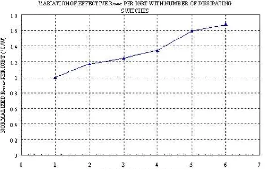
Thermal issues in power modules can be different that those usually found in discrete parts. This is due to in-teraction between the heat flow paths of individual die within the power module. Figure 7 simplistically represents the ther-mal scenario for a power module containing multiple power dissipating IGBTs and diodes. All the die are mounted on a single substrate, which serves to electrically isolate the high voltage devices from the case of the module. The substrate, in most cases, unfortunately also presents a high thermal resistance to the flow of heat to the heat sink. As shown in the figure, heat spreads away from the power die at an angle that depends upon many factors including substrate mate-rial and quality of interface with the heat sink. Usually it is approximated to about 45 ° on all the sides of the die. It is easily seen from the figure that the heat dissipated through the region ‘A’ of the substrate increases as more die start to dissipate. Thus the effective thermal resistance of each power die as seen from the module case increases with number of dissipating die. The rate at which the effective thermal resistance increases with number of dissipating die depends on the heat-spread angle, the closeness of power die in the module and the actual power dissipated.
An example of effective thermal resistance varia-tion with number of conducting die.is shown in figure 8. These results were obtained from a finite element thermal simula-tion performed on a substrate bearing IGBT/diode die. The thermal resistance for an IGBT under such circumstances varies significantly from the case with one IGBT dissipating to that with all six IGBTs in 3-phase inverter configuration dissipating. It should be noted that even though the IGBTs do not actually dissipate DC power simultaneously, the
ther-mal time constants for the system are long enough for heating effects to be similar.
The power die in IRAMS modules are optimally lo-cated so that thermal interaction between them is minimal. Also, the thermal resistance RTHJ-C specified in the IRAMS datasheet is under actual running conditions with all the IGBTs and diodes dissipating power. A good estimate of the minimum value of RTHJ-C can be made using the physical dimensions and thermal properties of the module layers. An example of this using a spreadsheet model is shown in table 2.
In the table, assuming a heat spread angle of 45 ° on all sides of the die, the equivalent area of heat conduction can be calculate odule stack-up. Then knowing the material thermal resistivity, the thermal resistance to heat flow path can be calculated. Starting from the active silicon area with dimensions given by side 1 and side 2, and the thickness of material, thermal resistance for that layer is given by
RTH
(
side x)(
sidet y)
∆ + ∆ + =2 1
.
ρ
(15)
AN-1044
Table 2. Spreadsheet model to calculate IGBT thermal resistance in power module Figure 8: Variation of effective IGBT thermal resistance with number of dissipating die
Dimension Side 1
inches
Side 2 inches
Side 1 m
Side 2 m
Area m2
Thickness m
Rth °K/W
0.080 0.080 2.03E-03 2.03E-03 4.13E-06
0.089 0.089 2.26E-03 2.26E-03 5.11E-06
Solder 0.101 0.101 2.57E-03 2.57E-03 6.58E-06 1.00E-04 0.28
Copper 0.108 0.108 2.74E-03 2.74E-03 7.53E-06 7.00E-05 0.02
Dielectric 0.114 0.114 2.90E-03 2.90E-03 8.38E-06 5.00E-05 1.49
Aluminum 0.281 0.281 7.14E-03 7.14E-03 5.09E-05 1.50E-03 0.14
HTC Plastic 0.326 0.326 8.28E-03 8.28E-03 6.86E-05 4.00E-04 2.34
Zth Total 4.45
Starting Active Area
AN-1044
Thermal Design (heat-sink selection)
The choice of heat-sink begins with the choice be-tween free convection and forced air cooling. For the lower powered appliance drives, such as washing machines, the motor drive is located near the base of the enclosure and free convection is usually employed. Refrigerators and air conditioners use a condenser fan which can provide addi-tional forced air cooling for the heat-sink. Heat-sinks de-signed for free convection airflow have taller, wider spaced fins than those for forced air operation and are about 50% larger for a given thermal resistance than a forced air heat-sink. The next consideration is the actual power to be dissi-pated and the allowable temperature rise above the ambi-ent air temperature. This results in an overall thermal resis-tance value in degree per watt which usually specifies sev-eral possibilities of fin configuration and lengths of heat-sink extrusion. The designer then chooses the most suitable heat-sink to comply with the mechanical constraints of the appli-cation. In any system having a heat source and a final heat-sink, in this case the semiconductor die inside the module and the ambient air, there has to be a temperature differ-ence ∆T which causes heat flow and a thermal resistance which determines the magnitude of the heat flow. An equiva-lent electrical circuit is shown below:
Rdie attach + R copper+ R insulation + R sub-strate + R molding compound are lumped together to form Rth(j-c) stated on the data sheet for each leg of the 3 phase inverter. Rcase-sink typically adds another 0.1°C/W with a correct application of thermal compound such as Wakefield Engineering # 120 HS Compound. The peak junction tem-perature where allowable power dissipation derates to zero is 150°C as stated on the data sheet. A prudent design would operate this module within a temperature range of Tj not exceeding 125°C worst case.
Design Example:
Operation of a 750Watt A/C compressor from a 400VDC regulated bus (boost topology PFC) using the IRAMS10UP60B module driven at 3.3KHz. The worst case ambient temperature is 40°C max. What heat-sink should I use to maintain Tj max = 125°C?
The maximum obtainable voltage from a 400VDC bus assuming 80% modulation depth is 320V p-p.and the rms voltage equivalent is 0.707 x 160 = 113VAC per phase. To generate 750W from 113VAC, the average current is 3.1A.
From the power loss calculation method described earlier, the following results are obtained for the above ex-ample:
Average switching power loss per IGBT Psw = 0.32 W Average conduction power loss per IGBT Pcond = 1.49 W Average power loss per diode is Pd = 0.53 W
From the above numbers, total power loss including all 6 IGBTs and diodes is Ptot = 14.1 W
IGBT thermal resistance from junction to case for the module IRAMS10UP60 is 4.7 °C/W as specified in the datasheet. It is assumed that heat is transferred to the heat sink uniformly from the module case. Thermal resistance from the module case to heat sink is approximately 0.1 °C/ W. Then the temperature rise of the IGBT junction above ambient is given by the following equation:
) (
)
( SW COND TOT THC S THS A
C THJ A
J T R P P P R R
T − = − + + − + − (16)
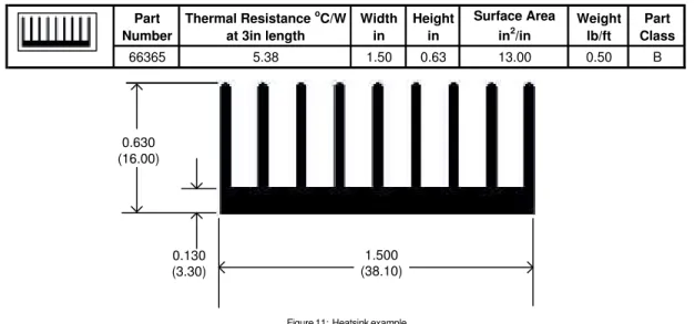
Substituting the above numbers in equation (16) with a de-sired Tj of 125 °C and an ambient of 40 °C, the thermal resistance of the heat sink to ambient comes to 5.42 °C/W. The heat sink shown in figure 11 is a standard part from Aavid/Thermalloy # 66365. With 3-inch length, it gives a ther-mal resistance of 5.38 °C/W from heat sink to ambient in free air convection. Thus the maximum junction tempera-ture requirement is met.
Thermal Diagram
SEMICONDUCTOR
SOLDER REFLOW DIE ATTACH COPPER CONDUCTOR DIELECTRIC LAYER METAL SUBSTRATE OVERMOLDING
HEAT SINK
MOLDING COMPOUND LAYER
POWER SEMICONDUCTORS
HEAT SOURCE HEAT SINK
R DIE ATTACH R COPPER R INSULATION R SUBSTRATER MOLDING COMPOUNDR CASE TO SINK
HEAT FLOW
AN-1044
Packaging and Installation Guide.
The IRAMS modules are intended to be soldered into a printed circuit board, which in most cost sensitive prod-ucts means a single sided PCB. Some inverter layouts, typi-cally those used with natural convection cooling in washing machines, mount the heat-sink vertically at one edge of the circuit board using the straight pin version of the module. Forced air cooled applications such as split system air con-ditioners commonly mount the PCB parallel to the heat-sink using the 90° bent pin module configuration. The module mounting screws are then made accessible through clear-ance holes drilled in the PCB positioned above the module.
Mounting screws can be 6-32 NC or M3 torqued to a nominal 6 inch-pounds. The mounting surface of the mod-ule is electrically isolated by a thin layer of thermally con-ductive molding compound. The thickness of this layer is
carefully controlled during the molding process so that a uniformly low thermal resistance (3°C/Watt) can be main-tained.
A heat-sink compound such as Wakefield Engineer-ing #120 applied in a thin layer is strongly recommended for maximum heat flow into the heat-sink. However, for low power applications it may be omitted. Without heat-sink com-pound, the flatness and surface finish of the heat-sink greatly influences the thermal resistance of this interface. The mounting force also affects thermal resistance, so it is im-portant to torque the mounting screws to 6in-LB or 0.7 Nm to ensure adequate contact. Spring clips can also be used to apply the required mounting force and provide a cost ef-fective alternative to screw mounting when used in large volume production.
Figure 12: Module mounting method
IRAMS Module PWB
Clearance Hole
Finned Heat-sink
90° LEAD-FORM MOUNTING
Forced Air Cooling Finned
Heat-sink
IRAMS Module
PWB
STRAIGHT PIN MOUNTING
Natural
Convection
Figure 11: Heatsink example
Part Number
Thermal Resistance oC/W at 3in length
Width in
Height in
Surface Area in2/in
Weight lb/ft
Part Class
66365 5.38 1.50 0.63 13.00 0.50 B
0.630 (16.00)
0.130 (3.30)
AN-1044
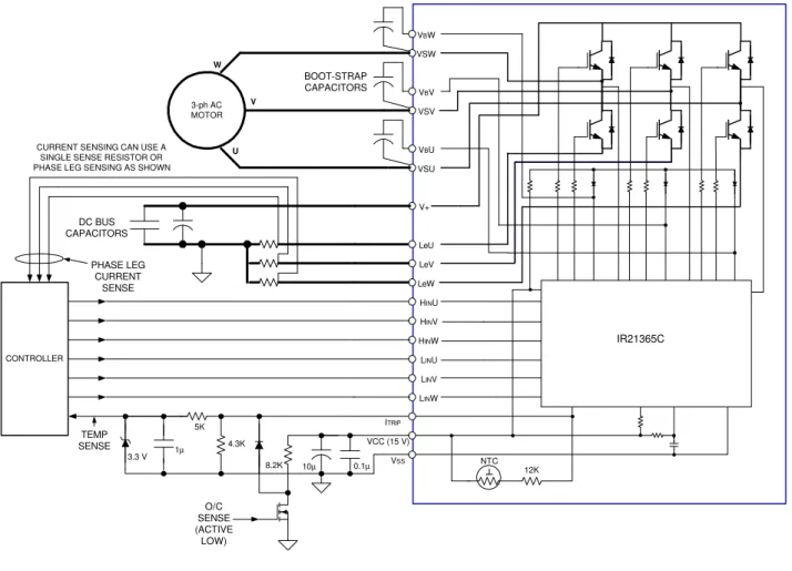
THE SYSTEM SCHEMATIC
A typical appliance or small industrial motor drive is shown in Fig. 13. The micro controller provides all of the logic level PWM signal inputs to the IRAMS module as well as processing current and temperature analog signals fed back from the module. The system schematic also dem-onstrates the simplicity of the drive and the small number of additional external components required. Note that no high-side floating power supplies are required because the bootstrap capacitors provide power for the three inde-pendent high side driver channels.
Motor current is monitored by external current sens-ing resistors in each phase leg of the IGBT inverter, but if ground fault detection is not required, a simplified current sensing can be provided by a single sense resistor. Under normal operating conditions, IGBT temperature is continu-ously monitored by the internal NTC thermistor feeding a temperature dependent voltage to the micro processor. This voltage also feeds the internal shut down function of the
driver which terminates all 6 drive signals when activated. In the event of an over current caused by a stalled motor or other fault condition, the active low signal from the micro controller turns off the external N-channel MOSFET and over rides the temperature signal causing instant shut down. Af-ter shutdown the 1.5Ω/6.8nF network provides a reset func-tion to re-establish IGBT gate drive following a 9mS delay. The micro processor can be programmed to provide per-manent termination of its outputs following a predetermined number of resets.
The sections so far described aspects of the sys-tem that directly affect the power module operation or se-lection, like bootstrap circuit, power losses within the mod-ule and thermal issues within and outside the modmod-ule. The next sections briefly explain elements of the system that, no doubt, are important but do not determine or are not deter-mined greatly by internal features of the module. These in-clude the housekeeping power supply and DC bus capaci-tors.
VCC (15 V) ITRIP
VSS
3.3 V NTC
12K 5K
1µ
CONTROLLER
3-ph AC MOTOR
LINW HINW
LINU
LINV LeW
HINU
HINV LeU
LeV V+ VSU VBU VSV VBV VSW VBW
IR21365C
DC BUS CAPACITORS
PHASE LEG CURRENT
SENSE
TEMP SENSE
BOOT-STRAP CAPACITORS
O/C SENSE (ACTIVE
LOW)
10µ
4.3K
8.2K W
V
U CURRENT SENSING CAN USE A
SINGLE SENSE RESISTOR OR PHASE LEG SENSING AS SHOWN
0.1µ
AN-1044
The rms current can also be calculated using equation (21) below.
. 2
rect DC DCpeak
DCrms I t f
I = (22)
The rms ripple current in the capacitor is given by equa-tion (23) below.
2 2
DCRMS CRMS
RMS I I
I = + (23)
The actual power loss in the capacitor is a function of its ESR at the ripple frequency of 100Hz or 120Hz depending on the mains frequency.
Hz RMS LOSS I ESR
P 100
2
= (24)
Controlling Capacitor Over Voltage
Capacitors can be destroyed if they are exposed to voltages in excess of their ratings due to line transients etc. An over voltage can also occur when capacitors are
connected to an LC- filter. See Figure 15.
Figure 15: Capacitor ring-up in L-C Circuit.
The ringing waveform is shown in Figure (16) below.
VC
VN
Figure 16: Voltage over shoot on the capacitor due to LC ring-up.
To avoid the voltage ringing when connecting the capaci-tors to the input network, it is advisable to use a soft start technique. Figure 17 shows two soft start networks. The soft start network 17(a) uses a self heating NTC thermistor or Surgistor for low power applications such as washing ma-chines. For higher power applications up to 2.5KW, the cir-cuit of (17)b can be used. A current inrush limiting resistor R is used and then shorted by a relay contact when the charg-ing current decays.
Bus Capacitor calculation
An electrolytic capacitor is used to smooth the rec-tified AC voltage from the bridge rectifier. Its capacitance is an inverse function of the allowed ripple voltage DV and can be derived from equation (17) below.
(17)
Where Pin is the load power in watts and DV is Vmax-Vmin.
Vmax
Vmin
t = 1/frect.
tc
tDC
Figure 14: Rectified AC Waveform Showing Conduction period from Vmin to Vmax.
It should be noted that electrolytic capacitors age and lose some capacitance over time and that the tolerance of the initial capacitance value should also be considered at the time of selection.
When using a capacitive input filter, the capacitor value not only determines the ripple voltage but also the conduction angle of the rectifier. The input voltage is sinusoidal and the expression (18) shows the charging time:
in c
f V V
t π
2 cos
max min 1
=
−
(18)
where fin is the line frequency.
The capacitor voltage discharge time tDC :can also be calculated from equation (19) below.
c rect
DC t
f
t = −
.
1
(19)
The average value of the charge current is given by:
c c
Cpeak
t V V C t
V C
I = ∆ = max− min
(20)
Equation (20) defines the average current drawn from the input rectifier and will be used in the selection of the rectifier diodes.
f t I ICrms= Cpeak2 c
(21)
(
)
rectin
f V V
P
C 2
min 2 max min
2
AN-1044
DC 220 VRMS
Input Bridge EMI
T
DC 220 VRMS
Input Bridge EMI
DC
Control
220 VRMS
Input Bridge EMI
(a)
(b)
(c)
Vbus=300VDC
D C
Input Bridge
DC
Control
Vbus=300VDC
Input Bridge
T
DC
Control
Vbus=300VDC
Input Bridge
(a)
(b)
(c)
tional AC solution where the transformer turns ratio de-fines the isolated DC bias voltage supplied by the bridge rectifier and capacitor. Of course, the output is unregulated and tracks the input line variations. Fig. 19b shows a non-isolated AC-DC step down approach suitable for low power bias applications. A dropping resistor provides the current source and the zener diode provides shunt regulation for the output voltage. Fig. 19c provides the most efficient solution, regulating the output voltage for line and load varia-tions. Since this is a high frequency PWM solution, the transformer size can be greatly reduced compared with the mains frequency solution.
The DC-DC solution may be also implemented by three different configurations. Fig. 20a is a linear regulator providing 15V bias, but this circuit suffers from the same high dissipation problem as the circuit of Fig.19b . It would dissipate 120W with a 0.4A load. The PWM solution is the most efficient and reliable way to provide the bias voltage as shown in Figs. 20b and 20c. The buck configuration pro-vides the non isolated approach, while the fly back configu-ration provides isolated outputs. The buck converter is the most efficient DC-DC converter and stresses the switching element to Vin but is non isolated. The flyback circuit stresses the primary switch to input voltage + reflected output volt-age + leakvolt-age inductance voltvolt-age spikes which are attenu-ated in a dissipative snubber or spike clipper circuit. A typi-cal flyback converter with 300VDC input requires a switch rating of about 800V.
The main DC bus filter capacitor attenuates the switching noise injected back to the input line by the PWM converter. This is a big advantage compared with the AC-DC solution of Fig.19c
Auxiliary Power Supply
In the appliance motor drive the auxiliary power supply provides 3.3VDC or 5VDC power to the micro con-troller and supplies +15V bias to the IGBT gate drivers and other users such as relays and indicator LEDs. Indi-vidual systems may have variations but the most com-mon solutions use +5V and +15V auxiliary power. In some cases, these voltages are required to be floating to pre-vent circulating currents in their return connections.
V
AC input
Input
Rectfier
Bus
Capacitors EMI
Input Filter
DC
A B
Figure 18: Power input path
Loads may be inserted at either point A or B depending upon whether an AC/DC or DC-DC converter is used to supply auxiliary power to the system as shown below in Figs. 19 and 20.
The AC-DC solution may be implemented by three different configurations. Fig. 19a shows the
tradi-Figure 19: AC-DC insertion in the input path.
Figure 20: DC-DC insertion in the input path. Figure 17: Soft start networks to avoid capacitor voltage overshoots
R L
C L
NTC
(a) (b)
AN-1044
The IR Solution
Since the IPM module incorporates its own level shifting, 3 phase driver, the auxiliary power supply can be referenced to the negative bus and does not require iso-lated outputs.
Consumer applications are very much cost driven so the non isolated buck solution is very attractive.
Buck Converter Design
A Synchronous buck topology will be shown using the IR 2153 IC. This is a 600V, high speed, self-oscillating level shifting driver with both high and low side referenced output channels. The front-end features a programmable oscillator similar to the ubiquitous CMOS 555. The output drivers feature a high pulse current buffer stage and an in-ternal dead time designed for minimum driver cross con-duction when driving MOSFETS in a ½ bridge or synchro-nous buck configuration.
Using the estimates from equations (1) thru’ (3) above, Table 1 gives a total power output for the auxiliary power supply of 4.8W.
Table 3 Output Requirements of Auxiliary Power Supply
Vin Vs
-L
C Ro
Sw
+
-Vout + +
Figure 21: Buck converter circuit
The output voltage of an ideal buck converter is a function solely of input DC voltage and duty cycle D, so long as the inductor L is in continuous conduction.
Vout = Vin x D
In a practical circuit the components have losses so the re-lationship becomes:
(28)
Power Analysis
To define the power requirements of the auxiliary power supply we need to evaluate the sources of power loss.
· Drive losses for the power switches. · Power requirements for signal generation. · Driver IC quiescent losses and level shift losses. · Bootstrap diode loss.
· Other losses such as indicator LEDs and relays etc.
Since there are 6 IGBT switches, the drive losses Ps are:
Ps =6 x Qg x Vge x f (25)
Where Qg is the charge needed for one turn on turn off cycle of one IGBT, Vge is the amplitude of the gate emitter voltage and f is the PWM frequency. In a worst-case sce-nario the value Qg is 80nC in the module family, the maxi-mum allowed gate voltage is 20V and the frequency in the appliance application is a maximum of 20kHz. Conductor power loss in bootstrap diodes is given by :
Pd =3 x Qd x Vd x f (26)
where Qd is the charge delivered through the bootstrap di-ode to charge the bootstrap capacitor. Vd is the didi-ode drop and f is the PWM frequency. These diodes are contained within the module so all the diode parameters are defined and fixed in the IRAMS data sheet. The Qd value is 100nC, the maximum forward voltage is 1V and the frequency value is still 20kHz. Sustituting in equation (26)
Pd ≈ 6mW.
The total power dissipated at the IC drivers is:
Pt = Ps+Pd+Pic = 200mW+6mW+100mW = 306mW (27)
A reasonable design safety margin, would be to double the result in equation (27) plus some auxiliary power for signal conditioning. This gives a total power estimate of < 1W for the 15V auxiliary power supply.
An estimate of the power requirements for the con-trol function using a micro concon-troller and E2prom or a Pic
microprocessor would be about 1W. To process the feed-back signals some signal conditioning circuitry has to be added around the controller. A good estimation is 0,5W for the peripheral circuitry. The total 5V power is about 1.5W to
the control section.
( )
in in s s Ts
s s s
out DTV DV
T dt t v T v
V = =1
∫
=1( )=0
P o w e r ( W ) I C d r i v e r 0 . 3 C o n t r o l S e c t i o n 1 . 5 L i n e a r R e g u l a t o r
AN-1044
age Vcc is internally regulated to 15.5V and switching takes place at 1/3 and 2/3Vcc just as in the generic 555 timer. The oscillator frequency is shown below :
(
RT)
CTf Ω + = 150 4 . 1 1 (31)
The Regulator Control Loop
Refering to Fig. 23 below, we see that the com-plete regulator schematic includes a TL 431 programmable shunt regulator IC. This regulator produces a high gain con-trol loop and concon-trols the duty cycle as a constant off time regulator. The high side switch duty cycle is large when the input voltage is low and small at high input voltage. Thus it can be seen that the constant off time control results in low frequency operation at 33.45V input and high frequency operation at 400V input. It is also noted that the TL 431 by-passes some charging current from C2 and thus increases its charge time to maintain voltage regulation of the +15V output. If we choose to operate at 50KHz and, the values from equation (31) are:
Under these conditions we see that:
kHz f ns T s T and T T f T T T D T T T D sw on off off on sw off on on off on on mn 99 507 11 1 max max min min min max max min max = = = + = + = + = µ (32) Inductor Calculation
In continuous conduction, the minimum inductance value is given by equation (33) below.
(
)
(
)
HkHz f D R L sw out µ 537 50 * 2 05 . 0 1 * 5 . 56 2 1 min min max min = − Ω = −
≥ (33)
In order to select the correct inductor the inductor peak current has to be calculated by the expression (34)
A H V s V L V T R V
I off out
out out
pk 0.54
600 * 2 15 * 11 5 . 37 15 2 min = + Ω = + = µ µ (34) In operation, the amplitude of the switching voltage Vs is
equal to the input DC voltage minus the switch saturation voltage drop Vsw plus the diode forward conduction voltage Vf in times respectively switch on and off.
A specification for the auxiliary power supply is shown be-low in Table 4.
Table 4. Power Supply specification
For practical purposes, the maximum duty cycle obtainable from the IR2153 is about 45%. Using the values shown in Table 4, the minimum input voltage is:
V V
D V
V out
in 33.45
45 . 0 15
max
min= = = (29)
At the other end of the scale, the DC bus voltage from a boost topology PFC preregulator is up to 400V. The duty cycle corresponding to this condition is determined from equation (30). Thus we can confidently predict that the auxiliary power supply can operate safely from a DC input of 40V to 400V.
% 75 . 3 400 15
min= = =
V V V V D inax out (30)
The IR2153 self oscillating driver IC uses the values of Rt and Ct to determine its oscillation frequency. Its supply
volt-Figure 22: Ct waveform and Output Timing Diagram of IR2153
nF C k R T T 7 . 2 1 . 5 = Ω =
P o w e r S u p p l y S p e c i f i c a t i o n
AN-1044
Ipk Value PKG
Inductance 0.5A 560 mH Power Inductor
Table 5: Specification of Inductor
VDSS PDSS @ 25
o
C Rds(on) @ 150
o
C PKG
500V 3.3A 3.0Ω Dpak
Table 6: Specification of Inductor
The Ipk of 4.5A is the value that will be used to calculate the inductance value of L1 and also the MOSFET switches used in the power supply.
The IRFR420A is a 500V surface mount MOSFET which can be used both as high side and low side switches in the synchronous buck converter.
VB VCC
RT
CT
COM HO
VS
LO R2
5k1
C2 2.7nF
R5 1k R3 22 +34V to +350V
COM
R1 470k 0.5W
D1 1EMU06
IRFR420A
L1 560uH 0.5A C4 47uF 450V
R7 2.7k R6 15k
C5 1000uF
25V
15V
C1 4.7uF
25V
C3 0.1uF
Q1
5V U2 7805
IR2153 U1
C6 10uF
25V C7
0.1uF
D3 1N4148
D4 1EMU06
Com pon e n t s V a lu e D e scr ipt ion Pr e cision , Pa r t n u m be r
R1 470k, 0.5W Resist or 5%
R2 5.1k Resist or 1%
R3, R4 22 Resist or 1%
R5 1 k Resist or 5%
R6 15k Resist or 1% R7 2.7k Resist or 1%
C1 4.7µF, 25V Elect rolyt ic
C2 2.7nF, Ceram ic
C3,C7 100nF Ceram ic
C4 47µF, 450V Elect rolyt ic
C5 1000µF, 25V Elect rolyt ic
C6 10 µF, 25V Elect rolyt ic
D1,D4 600V, 1A Diode 1EMU06, ( I R)
D2 Reference
zener diode TL431C
L1 560µH, 0.5A I nduct or
Q1 500V, 1A Mosfet I RFR420A ( I R)
U1 Cont rol I C I R2153 ( I R)
U2 1A Linear
regulat or LM7805
Figure 23: Power Supply Schematic
Note: Proper grounding layout for this circuit must be considered. All components must be kept as close as possible to each other and all traces must be kept to minimum to avoid stray capacitance and grounding noise
D2 TL431C
AN-1044
General Low Side Current Sensing
Introduction
The low side emitters, in the IRMAS10UP60A, are not tied together, which allows either the micro con-troller or the DSP to monitor the currents by external cur-rent sensing resistors in each phase. The purpose of these notes is to show a peculiar solution for feeding the cur-rent feedback to the A/D converter in the control scheme.
Problem analysis
When the shunt resistors are connected between the IGBT emitter and negative bus (Vbus-), the phase current is sensed in each leg. Figure 25 shows a typical schematic
The voltage signals are easier to be manipulated than current signals, so the shunt resistor works like a current to voltage transducer.
In a typical motor drive application, the voltage sensed by the shunt resistor can be either positive or nega-tive when referred to the Vbus-. The A/D converter must have positive input signals only. This is a big limitation and doesn’t allow the designer to use the shunt voltage information directly.
Solution
The signal supplied by the shunt resistor has to be compatible with the A/D input dynamic. It needs to be offset by a suitable value, thus the obtained signal is posi-tive in all the current range. For instance the transfer func-tion might be like the one shown in Figure 26.
Current feedback Signal condition general circuit (Figure 24)
Such transfer function can be implemented by the schematic shown in Figure 24. It is a peculiar differential amplifier with two inputs signals. The first one is the differen-tial mode value and the second one is the offset value.
Some assumptions were done to have a simple ex-pression of Vo/Vin. Figure 24 reports the relationships among the resistors in order to have:
(35)
Where Vdis the input signal or the shunt resistor drop, Rb=R5
and Ra=R2 select the voltage gain, Vrand the ratio R3/(R3+ R4) set the input offset needed.
The final circuit performance is related to the op-amp characteristics. It has to be Rail-to-Rail input/output in order to use the entire output dynamic. It needs a GBW > 1MHz, good slew rate > 0.5V/µV and low input offset voltage. It might be too expansive, but for instance the TLV2460 fits the request of the application.
Two examples, useful for the IRAMS10UP60A appli-cation, are reported in this paper.
Figure 25 shows the typical three-shunt current feed-backs using the IRAMS10UP60 power module. The shunt volt-age amplitude is related to the shunt value itself and the maxi-mum current through it. The IRAMS10UP60A datasheet re-ports the max peak current allowed is 15A. As advised in the application note AN1044, the designer has to provide an ex-ternal circuit that feeds the T/Itrip pin to shut down the system as soon as the current goes close to the max value. The
pro-(
3 4)
3
R R
R V R R V
V r
a b d out
+ + =
Typical example circuits
Typical low side current sensing circuit (Figure 25)
V+
V
-SHUNT- SHUNT+
+
-R1
R2 R3
R4
R5
VCC
VOUT
DGND Vr
I f R1= R2= Ra R5= R3/ R4= Rb Ra> > Rb
Vd* Rb
VOUT= Ra
+ Vr* R4
AN-1044
tection loop must shutdown the system faster than 10 µs otherwise the IGBTs will not survive the fault.
Using a rail-to-rail op-amp the circuit can read cur-rent up to 12.5A using 10mΩ as shunt resistors. Figure 27 shows the final amplifier configuration when the logic cir-cuitry at 5V. The voltage amplifier gain is 20. From the expres-sion (35) the input voltage is:
(36)
(37)
The values in (36) and (37) define the input dynamic of the differential amplifier. Assuming that during the start up phase the system runs at 12.5A, the RSHUNT is:
(38) Ω = = = m A V I V R LEG d SHUNT 10 5 . 12 125 . 0
Vout vs. Vshunt in Current Feedback signal condition circuit
0 1 2 3 4 5 6
-0.15 -0.1 -0.05 0 0.05 0.1 0.15
Vshunt
Vdsp
G=20 Vcc=5V
G=13.2 Vcc=3.3V
Figure 27: Current Feedback Signal condition circuit: Vcc=5V Gain=20
Figure 28: Current Feedback Signal condition circuit: Vcc=3.3V Gain=13.2
Signal condition transfer function (Figure 26)
( ) ( ) V
k k k k k V V R R R R R V V V b a r outM
d 0.125
9 . 49 49 . 2 100 100 100 5 5 4 3 3 max = Ω Ω Ω + Ω Ω − = + − =
( ) ( ) V
k k k k k V V R R R R R V V V b a r outm
d 0.125
9 . 49 49 . 2 100 100 100 5 0 4 3 3
min =−
Ω Ω Ω + Ω Ω − = + − =
The expression (38) defines the RSHUNT value in
order to have a range of +/-12.5A in the application. The circuit suggested in Figure 27 has good bandwidth up to 50kHz. It is wide enough for current sensing. If the user wants to change it, he has to play with C2 and C3. Keep in mind that the relationship Z3= Z4, in order to change C2
and C3, has to be mantained
The reader can do the same consideration on the circuit shown in figure 28 to evaluate the character-istics. Basically the circuit has the same performance of the circuit showed above using 3.3V voltage.
-0.15 -0.1 -0.05 0 0.05 0.1 0.15
+
-R4= 1.49k, 1%
R5= 100k, 1%
R6= 100k, 1%
R7= 49.9k, 1%
5V
VOUT
DGND C2= 100p
C3= 100p
R2= 1.49k, 1%
R1= 1k, 1%
R3= 1k, 1%
5V
C1= 1.1n
+
-R4= 1.49k, 1%
R5= 66k, 1%
R6= 66k, 1%
R7= 33k, 1%
3.3V
VOUT
DGND C2= 100p
C3= 100p
R2= 1.49k, 1%
R1= 1k, 1%
R3= 1k, 1%
3.3V
AN-1044
The information presented in this application note is believed to be accurate and reliable. However, International Rectifier can assume no responsibility for its use nor any infringement of patents or other rights of third parties which may result from its use. No license is granted by implication or other use under any patent or patent rights of International Recitifier. No patent liability shall be incurred for use of the circuits or devices described herein.