JOURNAL OF NANO- AND ELECTRONIC PHYSICS Р А А - А Р
Vol. 8 No 4(1), 04037(4pp) (2016) Том8№ 4(1), 04037(4cc) (2016)
2077-6772/2016/8(4(1))04037(4) 04037-1 2016 Sumy State University
Effects of High-
k
Dielectrics with Metal Gate
for Electrical Characteristics of SOI TRI-GATE FinFET Transistor
Fatima Zohra Rahou
*, A.Guen Bouazza, B. Bouazza
Department of Electronic and Electrical Engineering, Faculty of Technology, University of Abou-Bekr Belkaid, Tlemcen, Algeria
(Received 22 April 2016; revised manuscript received 22 November 2016; published online 29 November 2016)
In this paper, we present the results of a 3D-numerical simulation of SOI TRI-GATE FinFET transis-tor. 3D-device structure, based on technology SOI (Silicon-On-Insulator) is described and simulated by us-ing SILVACO TCAD tools and we compare the electrical characteristics results for Titanium Nitride (TiN) fabricated on Al2O3 (k ~ 9), HfO2 (k ~ 20) and La2O3 (k ~ 30) gate dielectric.
Excellent dielectric properties such as high-k constant, low leakage current, threshold voltage and elec-trical characteristics were demonstrated.
The implementation of high-k gate dielectrics is one of several strategies developed to allow further miniaturization of microelectronic components. From the simulation result; it was shown that HfO2 is the best dielectric material with metal gate TiN, which giving better subthreshold swing (SS), drain-induced barrier lowing (DIBL), leakage current Ioff and Ion/Ioff ratio.
Keywords: Technology SOI, Short-channel effects (SCEs), Multi-gate SOI MOSFET, SOI TRI-GATE Fin-FET, High-k dielectric, Silvaco Software
DOI: 10.21272/jnep.8(4(1)).04037 PACS number: 85.30.Tv
*f_rahou@yahoo.fr
1. INTRODUCTION
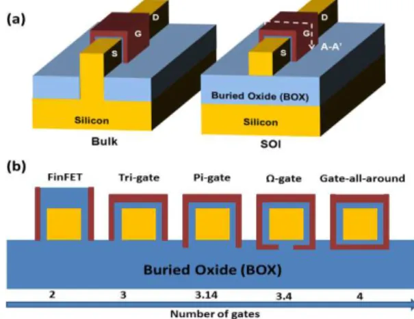
With down-scaling of CMOS, the short-channel ef-fects (SCEs) which are caused by the decreasing gate control over the channel are among the most important challenges in the semiconductor industry. In order to suppress the SCEs, novel device architectures have been proposed. Multiple-gate silicon-on insulator MOSFETS, have been proposed due to their ability to overcome several limitations like low speed and re-duced short-channel effects (SCEs). The most im-portant types of multiple-gate SOI MOSFET devices are summarized in (Figure 1), represented by the num-ber of gates around the channel.
Fig. 1– Schematic of (a) bulk and SOI multi-gate FETS, as well as, (b) cross-section of different multi-gate FETS and their corresponding effective number of gates [1]
The Fin field effect transistor (FinFETs) is a SOI based multiple gate structure, which is recently emerging as a leading structure to continue the scaling of CMOS
technology into the nanometer regime. This promising multiple gate structure has not only the advantage of reducing short channel effects but also of being compat-ible with the conventional planar CMOS technology. The two most important FinFET structures are the double-gate (DG) SOI MOSFETs and triple-gate (TG).
Of all SOI MOSFET structures, triple-gate transis-tors are very promising because it combines good sub threshold characteristics with high on-currents and are considered to be very good alternatives to planar devices.
Fig. 2– Schematic of SOI TRI-GATE FinFET
2. HIGH-K DIELECTRIC
Since the advent of the metal-oxide semiconductor system over 40 years ago, the SiO2 gate oxide has been
F.Z. RAHOU, A.G. BOUAZZA, B. BOUAZZA J.NANO-ELECTRON.PHYS. 8, 04037 (2016)
04037-2 have already proposed some applicable solutions, in-cluding new materials, new technologies and device structure innovation. The major advances in Nanosize materials with high-k gate dielectric and metal gate to solve the problems existing in the gate stack and the low power issue [2].
Replacing the SiO2 with a high-k material allows
increased gate capacitance [3]. The electrical character-istics of the device performance are analyzed with sev-eral of high-k materials and the gate oxide thickness is scaled to get same Equivalent Oxide Thickness (EOT) defined as equation (1):
(1)
Where:
TM1 and TM2 are the physical thickness of
metals-oxides M1 and M2, εM1 and εM2 are their relatives
die-lectrics constants respective, εSiO2 is relative dielectric
of the SiO2.
Recently, many researchers are focused on metal oxide materials with high-k values that have the ability to be integrated in MOSFET process flow. There are many high-k materials that are being studied nowa-days such as Al2O3, HfO2, and La2O3 [4]. The best
char-acteristics of gate dielectric should have high dielectric constant, large band gap with a favorable band align-ment, low interface state density and good thermal stability. Among the high-k materials are compatible with silicon, and also materials have too low or high dielectric constant may not be adequate choice for al-ternative gate dielectric [5].
Among the high-k dielectrics which are currently most promising, as their dielectric permittivity are referred in Table 1.
Table 1– High-k dielectrics with their dielectric permittivity
Material Dielectric permittivity
HfO2 20
Al2O3 9
Y2O3 15
La2O3 30
ZrO2 25
Among all the potential candidates for metal gate, TiN is widely studied because of its superior perfor-mance such as stability when contacted with high-k dielectrics, low resistivity, and process compatibility [6].
In this paper, we compare the electrical characteris-tics results for Titanium Nitride (TiN) fabricated on Al2O3 (k ~ 9), HfO2 (k ~ 20) and La2O3 (k ~ 30) gate
dielectric with Equivalent Oxide Thickness EOT = 1.2 nm .In this simulations, Titanium nitride (TiN) is used as gate contact material and the work function of metal is kept 4.45 eV.
3. DEVICE STRUCTURE
SOI TRI-GATE FinFET structures with using high-k dielectrics Al2O3, HfO2 and La2O3 are analyzed and
compared by using 3D numerical device simulator SILVACO TCAD. Figure 3 show 3D illustrations of both structures with the cross-sectional views.
The different parameters of our structure are
pre-sented in Table 2. The electrical characteristics of the devices were simulated using the Atlas Silvaco soft-ware [7].
Fig. 3– 3D device schematic view and Cross-section view of SOI TRI-GATE FinFET with TiN/1 nm Al2O3/0.8 nm SiO2 stack, TiN/2 nm HfO2/0.8 nm SiO2 stack and with TiN/3 nm La2O3/0.8 nm SiO2 stack
Table 2– The parameters used for the SOI TRI-GATE FinFET
Device Parameters
TiN /1 nmAl2O3 /0.8 nmSiO2
TiN /2 nm HfO2 /0.8 nm SiO2
TiN /3 nmLa2O3 /0.8 nm SiO2 Body Doping
Concentra-tion
5 1017[cm – 3] 5 1017[cm – 3] 5 1017[cm – 3]
Drain /Source doping
con-centration
5 1020[cm – 3] 5 1020[cm – 3] 5 1020[cm – 3]
Gate length 30 [nm] 30 [nm] 30 [nm] Equivalent
Oxide Thick-ness EOT
1.2 [nm] 1.2 [nm] 1.2 [nm]
Fin Width 10 [nm] 10 [nm] 10 [nm]
Fin Height 10 [nm] 10 [nm] 10 [nm] Buried oxide
thickness
20 [nm] 20 [nm] 20 [nm]
Substrate thickness
30 [nm] 30 [nm] 30 [nm]
Work func-tion ΦTiN
4.45 [ev] 4.45 [ev] 4.45 [ev]
4. SIMULATION AND RESULTS
4.1 Drain Source Saturation Current (Idsat)
Simulation results show that there is an increase in Id sat for SOI TRI-GATE FinFET when we use High-k dielectrics Al2O3 (k ~ 9), HfO2 (k ~ 20) and La2O3
(k ~ 30).
The devices have been simulated for a drain bias of 0 to 0.6 V and for a gate bias of 0.8 V (Figure 4).
Idsat for SOI TRI-GATE FinFET out to be 1.82 e– 5 A
with TiN/2 nm HfO2/0.8 nm SiO2 stack and 2.02 e– 5 A
with TiN/3 nm La2O3/0.8 nm SiO2 stack but reduced to
EFFECTS OF HIGH-K DIELECTRICS WITH METAL GATE J.NANO-ELECTRON.PHYS. 8, 04037 (2016)
04037-3
Fig. 4–IDS-VDS characteristics of SOI TRI-GATE FinFET with TiN/1 nm Al2O3/0.8 nm SiO2 stack, TiN/2 nm HfO2/0.8 nm SiO2 stack and with TiN/3 nm La2O3/0.8 nm SiO2 stack
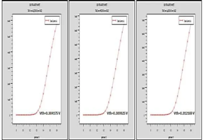
4.2 Input Threshold voltage (Vth)
Simulation results show increasing threshold volt-age for SOI TRI-GATE FinFET when we have use Al2O3, HfO2 and La2O3 as gate dielectric.
Threshold voltage has been calculated for drain source voltage of 0.1 V, while varying gate source volt-age from 0 V to 0.6 V (Figure 5).
Fig. 5 –IDS-VGS characteristics of SOI TRI-GATE FinFET with TiN/1 nm Al2O3/0.8 nm SiO2 stack, TiN/2 nm HfO2/0.8 nm SiO2 stack and with TiN/3 nm La2O3/0.8 nm SiO2 stack
Threshold voltage for SOI TRI-GATE FinFET out to be 0.304175 V with TiN/1 nm Al2O3/0.8 nm SiO2 stack
and to 0.309925 V with TiN/2 nm HfO2/0.8 nm SiO2
stack and to 0.312169 V with TiN/3 nm La2O3/0.8 nm
SiO2 stack.
4.3 Subthreshold Slope
Sub threshold slope or swing is an important pa-rameter reveals how better the device functions as a switch.
The lower the value of SS, the more efficient and rapid the switching speed of the device from the off state to the on state. It is easily seen that SS is the inverse of the slope of the weak-inversion part of the Log IDS vs VGS in Figure 6, the expression for sub
threshold slope is given by Equation (2) [8]:
(2)
Where dVGS is change in gate voltage, dIDS is change
in drain current.
Fig. 6 – IDS-VGS subthreshold voltage of SOI TRI-GATE FinFET with TiN/1 nm Al2O3/0.8 nm SiO2 stack, TiN/2 nm HfO2/0.8 nm SiO2 stack and with TiN/3 nm La2O3/0.8 nm SiO2 stack
Simulation results show that there is an improve-ment in subthreshold slope for SOI TRI-GATE FinFET with HfO2 dielectric compared to SOI TRI-GATE
Fin-FET with Al2O3 and La2O3 dielectrics.
Subthreshold slope for SOI TRI-GATE FinFET comes out to be 63.7591 mv/decade with TiN/1 nm Al2O3/0.8 nm SiO2 stack and to 63.4718 mv/decade with
TiN/2 nm HfO2/0.8 nm SiO2 stack and to 63.7113
mv/decade with TiN/3 nm La2O3/0.8 nm SiO2/stack.
4.4 Drain Source off Current (Ioff)
One of the biggest challenges faced by MOSFET scaling is high value of off state current or high leakage current resulting in high power consumption.
Simulation results infer that there is decrease in off state current for SOI TRI-GATE FinFET with HfO2
dielectric compared to SOI TRI-GATE FinFET with Al2O3 and La2O3 dielectrics.
F.Z. RAHOU, A.G. BOUAZZA, B. BOUAZZA J.NANO-ELECTRON.PHYS. 8, 04037 (2016)
04037-4 Off state current has been calculated for drain source voltage (VDS 1.2 V) and gate source voltage
from (VGS 0 V).
With the integration of high-k dielectrics into SOI TRI-GATE FinFET, the performance of the device is further enhanced and improved.
Off state current of SOI TRI-GATE FinFET out to be 6 e– 12 A with TiN/3 nm La
2O3/0.8 nm SiO2 stack
and to 5.79 e– 5 A with TiN/1nm Al2O3/0.8 nm SiO2 but
reduced to 5.6 e– 12 A with TiN/2 nm HfO
2/0.8 nm SiO2
stack.
4.5 Drain Source on Current (Ion)
On state current is also one of the important pa-rameter of a device, which determines fan out & fan in capabilities of a circuit, etc. Simulation results show that there is significant improvement in on state cur-rent for SOI TRI-GATE FinFET when La2O3 is used as
dielectric as compare to Al2O3 and HfO2 in SOI
TRI-GATE FinFET.
On state current has been calculated for drain source voltage (VDS 1.2 V) and gate source voltage
(VGS 1.2 V) (Figure 7).
On state current of SOI TRI-GATE FinFET out to be 3.53 e– 5 A with TiN/2 nm HfO
2/0.8 nm SiO2 stack
and to 3.72 e– 5 A with TiN/3 nm La
2O3/0.8 nm SiO2
stack but reduced to 2.88 e– 5 A with TiN/1 nm
Al2O3/0.8 nm SiO2.
4.6 Ratio of Drain Source on Current to Drain
Source off Current (Ion/Ioff)
The on/off current ratio is very important for the digital VLSI design. It will determine the speed-power performance parameter of the circuit. The higher the ratio, the better will be the performance of the circuit in terms of speed and power. Simulation results infer improvement in the SOI TRI-GATE FinFET with stacking TiN/2 nm HfO2/0.8 nm SiO2. The ratio has
been calculated for drain source voltage (1.2 V) and gate source voltage from 0 V to 1.2 V (Figure 7).
Ion/Ioff ratio of SOI TRI-GATE FinFET out to be 6.3 e6
with TiN/2 nm HfO2/0.8 nm SiO2 stack and to 6.2 e6 with
TiN/3 nm La2O3/0.8 nm SiO2 stack but reduced to 5 e6
with TiN/1 nm Al2O3/0.8 nm SiO2 stack.
4.7 DIBL (Drain Induced Barrier Lowering)
The fundamental electrical limitation in VLSI will be the spacing of the surface diffusions that form p-n junctions. Reverse bias on one diffused junction creates
a field pattern that can lower the potential barrier separating it from an adjacent diffused junction. When this barrier lowering is large enough, the adjacent diffusion behaves as a source, resulting in an unwanted current path.
It is obtained by carrying out the difference on threshold voltage for two voltages drain, a first is the low drain voltage (VDS1 0.1 V) and the second the high
drain voltage (VDS2 1.2 V).
| |
(3)
Fig. 8 – DIBL effect inSOI TRI-GATE FinFET with TiN/1 nm Al2O3/0.8 nm SiO2 stack, TiN/2 nm HfO2/0.8 nm SiO2 stack and with TiN/3 nm La2O3/0.8 nm SiO2 stack
DIBL of SOI TRI-GATE FinFET out to be 44 with TiN/1 nm Al2O3/0.8 nm SiO2 stack and to 42 with
TiN/3 nm La2O3/0.8 nm SiO2 stack but reduced to 40
with TiN/2 nm HfO2/0.8 nm SiO2 stack.
5. CONCLUSION
SOI TRI-GATE FinFET structures were successful-ly designed and stimulated to study the several dielec-tric materials on metal gate of device performance. The performance of the three dielectric materials, Al2O3,
HfO2 and Al2O3 with TiN as metal gate were compared.
HfO2 is the best dielectric material with metal gate
TiN, which shown better subthreshold swing (SS), drain-induced barrier lowing (DIBL), leakage current Ioff and Ion/Ioff ratio, for this reasons, HfO2 is the best
dielectric material for the future nano-scaleMulti-gate SOI MOSFETs devices technology.
REFERENCES
1. I. Ferain, C.A. Colinge, J.P. Colinge, Nature 479, 310
(2011).
2. T. Rudenko, V. Kilchytska, N. Collaert, M. Jurczak, A. Nazarov, D. Flandre, Sol. Stat. Elect. 51(11) (2007). 3. AH. Afifah Maheran, P.S. Menon, I. Ahmad, S. Shaari,
H.A. Elgomati, F. Salehuddin, J. Phys. Conf. Series 43, 012026 (2013).
4. H. Wong, H. Iwai, Micro. Engin. 83(10), 1867(2006).
5. B.H. Lee, L. Kang, W-J. Qi, R. Nieh, Y. Jeon, K. Onishi and J.C. Lee, IEEE Electr. Dev., 133, (1999).
6. F.Z. Rahou, A.G. Bouazza, B. Bouazza, IETE J. Res. 62(3), (2015)
7. Silvaco, ATLAS User’s Manual Device Simulation Soft-ware, Santa ClaraCA: Silvaco International (2012). 8. L. Ying, H. Jin, C. Mansun, D. Cai-Xia, Y. Yun, Z. Wei,