A Simplified Power Supply
Design Using the TL494
Control Circuit
Prepared by: Jade H. Alberkrack ON Semiconductor
Bipolar IC Division
This bulletin describes the operation and characteristics of
the TL494 SWITCHMODEt Voltage Regulator and shows
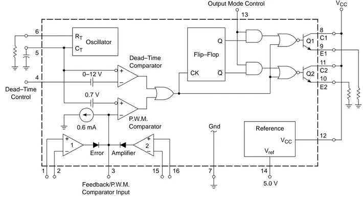
its application in a 400–watt off–line power supply. The TL494 is a fixed–frequency pulse width modulation control circuit, incorporating the primary building blocks required for the control of a switching power supply. (See Figure 1). An internal linear sawtooth oscillator is
frequency–programmable by two external components, RT
and CT. The oscillator frequency is determined by:
fosc^ 1.1
RT@CT
Output pulse width modulation is accomplished by comparison of the positive sawtooth waveform across
capacitor CT to either of two control signals. The NOR gates,
which drive output transistors Q1 and Q2, are enabled only when the flip–flop clock–input line is in low state. This
happens only during that portion of time when the sawtooth voltage is greater than the control signals. Therefore, an increase in control–signal amplitude causes a corresponding linear decrease of output pulse width. (Refer to the timing diagram shown in Figure 2).
The control signals are external inputs that can be fed into the dead–time control (Figure 1, Pin 4), the error amplifier inputs (Pins 1, 2, 15, 16), or the feedback input (Pin 3). The dead–time control comparator has an effective 120 mV input offset which limits the minimum output dead time to approximately the first 4% of the sawtooth–cycle time. This would result in a maximum duty cycle of 96% with the output mode control (Pin 13) grounded, and 48% with it connected to the reference line. Additional dead time may be imposed on the output by setting the dead–time control input to a fixed voltage, ranging between 0 to 3.3 V.
Figure 1. TL494 Block Diagram 6 5 4 Dead–Time Control Oscillator 0–12 V 0.7 V 0.6 mA + 1 – – + – + + 2 – Q CK 13 Reference Q1 Q2 8 9 11 10 12 VCC
1 2 3 15 16 7 14
Feedback/P.W.M. Comparator Input
Flip–Flop
Output Mode Control
Dead–Time Comparator P.W.M. Comparator Q Error Amplifier RT CT VCC Gnd Vref 5.0 V E2 C2 E1 C1
This document may contain references to devices which are no longer offered. Please contact your ON Semiconductor representative for information on possible replacement devices.
APPLICATION NOTE
Figure 2. TL494 Timing Diagram Capacitor CT
Feedback/P.W.M. Comp. (Pin 3) Dead–Time Comp. (Pin 4)
Flip–Flop Clock Input
Flip–Flop Q
Flip–Flop Q
Output Q1 Emitter (Pin 9)
Output Q2 Emitter (Pin 10)
Output Mode Control (Pin 13)
The pulse width modulator comparator provides a means for the error amplifiers to adjust the output pulse width from the maximum percent on–time, established by the dead–time control input, down to zero, as the voltage at the feedback pin varies from 0.5 to 3.5 V. Both error amplifiers
have a common mode input range from –0.3 V to (VCC –
2 V), and may be used to sense power supply output voltage and current. The error amplifier outputs are active high and are ORed together at the inverting input of the pulse width modulator comparator. With this configuration, the
amplifier that demands minimum output on time, dominates
control of the loop.
When capacitor CT is discharged, a positive pulse is
generated on the output of the dead–time comparator, which clocks the pulse steering flip–flop and inhibits the output transistors, Q1 and Q2. With the output mode control connected to the reference line, the pulse–steering flip–flop directs the modulated pulses to each of the two output transistors alternately for push–pull operation. The output frequency is equal to half that of the oscillator. Output drive can also be taken from Q1 or Q2, when single–ended operation with a maximum on–time of less than 50% is required. This is desirable when the output transformer has a ringback winding with a catch diode used for snubbing.
a thermal drift of less than 50 mV over an operating
temperature range of 0 to 70°C.
APPLICATION OF THE TL494 IN A 400 OFF–LINE POWER SUPPLY
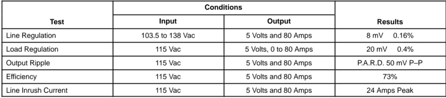
A 5 V, 80 A line operated 25 kHz switching power supply, designed around the TL494, is shown in Figure 3, and the performance data is shown in Table 1. A brief explanation of each section of the power supply is as follows:
AC Input Section
The operating ac line voltage is selectable for nominal of 115 or 230 volts by moving the jumper links to their appropriate positions. The input circuit is a full wave voltage doubler when connected for 115 VAC operation with both halves of the bridge connected in parallel for added line–surge capability. When connected for 230 VAC operation, the input circuit forms a standard full wave bridge.
coupled from the primary to the secondary of T3, forward biasing the base–emitter of Q3, and charging C3 through CR1. Resistor R3 provides a dc path for the ‘on’ drive after C3 is fully charged. Note that the emitter–base of Q2 is reverse biased during this time. Turn–off drive to Q3 commences during the dead–time period, when both Q6 and Q7 are off. During this time, capacitor C3 will forward bias the base–emitter of Q2 through R3 and R2 causing it to turn on. The base–emitter of Q3 will now be reverse biased by the charge stored in C3 coupled through the collector–emitter of Q2.
Output Section
The ac voltage present at the secondaries of T1 is rectified by four MBR 6035 Schottky devices connected in a full wave center tapped configuration. Each device is protected from excessive switching voltage spikes by an R–C snubber, and output current sharing is aided by having separate secondary windings. Output current limit protection is achieved by incorporating a current sense transformer T4. The out–of–phase secondary halves of T1 are cross connected through the core of T4, forming a 1–turn primary. The 50 kHz output is filtered by inductor L1, and capacitor C4. Resistor R4 is used to guarantee that the power supply will have a minimum output load current of 1 ampere. This prevents the output transistors Q3 and/or Q5 from cycle skipping, as the required on–time to maintain regulation into an open circuit load is less than that of the devices storage time. Transformer T5 is used to reduce output switching spikes by providing common mode noise rejection, and its use is optional.
The MC3423, U1, is used to sense an overvoltage condition at the output, and will trigger the crowbar SCR, Q8. The trip voltage is centered at 6.4 V with a programmed
delay of 40 ms. In the event that a fault condition has caused
the crowbar to fire, a signal is sent to the control section via jumper ‘A’ or ‘B.’ This signal is needed to shut down the
output, which will prevent the crowbar SCR from destruction due to over dissipation. Automatic over voltage reset is achieved by connecting jumper ‘A’. The control section will cycle the power supply output every 2 seconds until the fault has cleared. If jumper ‘B’ is connected, SCR Q12 will inhibit the output until the ac line is disconnected.
Low Voltage Supply Section
A low current internal power supply is used to keep the control circuitry active and independent from external loading of the output section. Transformer T2, Q9 and CR2 form a simple 14.3 V series pass regulator.
Control Section
The TL494 provides the pulse width modulation control for the power supply. The minimum output dead–time is set to approximately 4% by grounding Pin 4 through R5. The soft start is controlled by C5 and R5. Transistor Q11 is used to discharge C5 and to inhibit the operation of the power supply if a low ac line voltage condition is sensed indirectly by Q10, or the output inhibit line is grounded.
Error amplifier 1 and 2 are used for output voltage and current–level sensing, respectively. The inverting inputs of both amplifiers are connected together to a 2.5 V reference derived from Pin 14. By connecting the two inputs together, only one R–C feedback network is needed to set the voltage gain and roll off characteristics for both amplifiers. Remote output voltage sensing capability is provided, and the supply will compensate for a combined total of 0.5 V drop in the power busses to the load. The secondary of the output
current sense transformer T4, is terminated into 36 W and
peak detected by BR1 and C6. The current limit adjust is set for a maximum output current of 85 amperes.
The oscillator frequency is set to 50 kHz by the timing
components RT and CT. This results in a 25 kHz two phase
output drive signal, when the output mode (Pin 13) is connected to the reference output (Pin 14).
Table 1. 400 Watt Switcher Performance Data
Conditions
Test Input Output Results
Line Regulation 103.5 to 138 Vac 5 Volts and 80 Amps 8 mV 0.16%
Load Regulation 115 Vac 5 Volts, 0 to 80 Amps 20 mV 0.4%
Output Ripple 115 Vac 5 Volts and 80 Amps P.A.R.D. 50 mV P–P
Efficiency 115 Vac 5 Volts and 80 Amps 73%
Y
SECTION
POWER SECTION
T1
10 k 10 k
5 W 5 W
C1
2400 200 V
C2
2400 200 V
MDA 2504 100 5 W 100 5 W 0.001 1 kV 0.001 1 kV 1N4936 1N4936
4 200 V 4 200 V
TIP31
Q2 TIP31Q4
MJ13015 MJ13015 Q3 Q5 1N4933 1N4933 33 33 R2 330 10 V 330 10 V + + 5 3 W 5 V SEN
5 V 80 A 5 V SEN RTN 5 V RTN
Output 10 1/2 W 10 1/2 W 1N4001
2200 10 V
7.5 k 5.1 k
Inhibit MC3423 U1 7 5 4 3 8 1 + 50 V 0.0033 MBR6035 MBR6035 OUTPUT SECTION 0.05 0.05 10 10 1/2 W 1/2 W
MBR6035
MBR6035
0.05
0.05
10
10 1/2 W 1/2 W 1
L1 4.7 10 W
R4 T5 50 V 1 + 330
1 k 1 k
+ C4 46000 10 V
33 C 35 U
0.01 Q8 MCR 100.3 Q12 ‘A’ ‘B’ T4 11 5
230 T2 +
35 V 2200 1N4744 390 1 W
Q9 TIP31 + 16 V 1000 5.1 k 560 1.5 k 2.2 k
1N4933 1N4933 560 TIP32 Q6 Q7 TIP32 MPS A 70 Q10 1 4.7 k 10 1N4001 + 16 V 330 1N4001
8.2 k 0.001
50 V MPS A 55 Q11 TL494 U2 Output Voltage Adj.
8.2 k 4.7 k
36
1 W BR1
5 k 10 Turn 25 k 10 Turn 0.001 50 V 0.001 50 V 33 k
18 k 1N4001 C6 + 16 V 22 CT RT 0.003 16 5 6
1 3 15 2 14 13 10 9 7 8 12 11 4 18 k R5 0.1 10 k 10 k
8.2 k
0.01
50 V 1 MEG
47 50 V C5
All Capacitors in mF All Resistors in Ohms 1/4 Watt
(unless otherwise noted)
Current Limit
Adj. Set for 85
Transformer Data T1 Core:
Bobbin: Windings:
Ferroxcube EC 70–3C8, 0.002″ gap in each leg Ferroxcube 70PTB
Primary (Q3, Q5): Primary (Q1): Secondary, 4 each: Shield, 2 each:
50 turns total, #17 AWG Split wound about secondary. 4 turns, #17 AWG.
3 turns, #14 AWG Quad Filar wound. Made from soft alloy copper 0.002″ thick.
T2 Core: Bobbin: Windings:
Allegheny Ludlum EI–75–M6, 29 gauge Bobbin Cosmo EI 75
Primary, 2 each: Secondary:
1000 turns, #36 AWG. 200 turns, #24 AWG.
T3 Core: Windings:
Ferroxcube 846 T250–3C8 Primary, 2 each:
Secondary, 2 each:
30 turns, #30 AWG Bifilar wound. 12 turns, #20 AWG Bifilar wound.
T4 Core: Windings:
Magnetics Inc. 55059–A2 Primary, 2 each: Secondary:
1 turn, #14 AWG Quad Filar wound. Taken from secondary to T1. 500 turns, #30 AWG.
T5 Core: Windings:
Magnetics Inc. 55071–A2 Primary:
Secondary:
4 turns, #16 AWG Hex Filar wound. 4 turns, #16 AWG Hex Filar wound.
L1 Core: Windings:
TDK H7C2 DR 56 x 35
ON Semiconductor and are registered trademarks of Semiconductor Components Industries, LLC (SCILLC). SCILLC reserves the right to make
changes without further notice to any products herein. SCILLC makes no warranty, representation or guarantee regarding the suitability of its products for any particular purpose, nor does SCILLC assume any liability arising out of the application or use of any product or circuit, and specifically disclaims any and all liability, including without limitation special, consequential or incidental damages. “Typical” parameters which may be provided in SCILLC data sheets and/or specifications can and do vary in different applications and actual performance may vary over time. All operating parameters, including “Typicals” must be validated for each customer application by customer’s technical experts. SCILLC does not convey any license under its patent rights nor the rights of others. SCILLC products are not designed, intended, or authorized for use as components in systems intended for surgical implant into the body, or other applications intended to support or sustain life, or for any other application in which the failure of the SCILLC product could create a situation where personal injury or death may occur. Should Buyer purchase or use SCILLC products for any such unintended or unauthorized application, Buyer shall indemnify and hold SCILLC and its officers, employees, subsidiaries, affiliates, and distributors harmless against all claims, costs, damages, and expenses, and reasonable attorney fees arising out of, directly or indirectly, any claim of personal injury or death associated with such unintended or unauthorized use, even if such claim alleges that SCILLC was negligent regarding the design or manufacture of the part. SCILLC is an Equal Opportunity/Affirmative Action Employer.