Licenciada em Química
Label-free detection of biomolecules with
Ta2O5-based field effect devices
Dissertação para obtenção do Grau de Doutor em Nanotecnologias e Nanociências
Orientador: Doutora Elvira Maria Correia Fortunato, Professora
Catedrática, Faculdade de Ciências e Tecnologia da
Universidade Nova de Lisboa
Co-orientador: Doutor Pedro Miguel Ribeiro Viana Baptista, Professor
Auxiliar com Agregação, Faculdade de Ciências e
Tecnologia da Universidade Nova de Lisboa
Júri:
Presidente: Professor Doutor Fernando José Pires Santana Arguentes: Prof. Doutora Maria Goreti Ferreira Sales
Prof. Doutor Abel Martim González Oliva Vogais: Professor Doutor José Higino Gomes Correia
Prof. Doutor Guilherme Nuno de Passos Correia Matos Ferreira Professor Doutor Rodrigo Ferrão de Paiva Martins
Prof. Doutor Hugo Manuel Brito Águas
i
Licenciada em Química
Label-free detection of biomolecules with Ta2O5-based
field effect devices
Dissertação para obtenção do Grau de Doutor em Nanotecnologias e Nanociências
Orientador: Doutora Elvira Maria Correia Fortunato, Professora
Catedrática, Faculdade de Ciências e Tecnologia da
Universidade Nova de Lisboa
Co-orientador: Doutor Pedro Miguel Ribeiro Viana Baptista, Professor
Auxiliar com Agregação, Faculdade de Ciências e
Tecnologia da Universidade Nova de Lisboa
Júri:
Presidente: Professor Doutor Fernando José Pires Santana Arguentes: Prof. Doutora Maria Goreti Ferreira Sales
Prof. Doutor Abel Martim González Oliva Vogais: Professor Doutor José Higino Gomes Correia
Prof. Doutor Guilherme Nuno de Passos Correia Matos Ferreira Professor Doutor Rodrigo Ferrão de Paiva Martins
Prof. Doutor Hugo Manuel Brito Águas
iii
Label-free detection of biomolecules with Ta2O5-based field effect devices
Copyright: Rita Maria Mourão Salazar Branquinho FCT/UNL e UNL
v
It is said that scientific research is a lonely line of work but as I think back and look
around the lab there are many people that contributed to this work and to whom I
wish to thank.
First I want to acknowledge my supervisors for their support, advice and guidance
throughout this work. Their complementarity in scientific and teaching expertise and
their shared enthusiasm for science largely contributed to both my professional and
personal growth. Prof. Elvira Fortunato; for the opportunity to develop this new line
of work within the group, for her relentless efforts to provide all the necessary means
for the success of this research investing in lab facilities, international collaborations
and my own academic formation. Thank you for the trust you deposited in me and
my work. Prof. Pedro Baptista; for lively and fruitful discussions, for saying ‘you
know this won’t work!’ it was always uplifting and for providing the ‘sexy’ DNA
targets. Thank you for the confidence in me and my work.
To Prof. Rodrigo Martins, for allowing the development of this work in the research
facilities of DCM/FCT-UNL and for all his support.
To Dr. Joana Vaz Pinto and future Dr. Bruno Veigas, friends and companions in
endless lab work and whose contribution to this work was indispensable.
To former colleagues whose support and friendship surpassed distance; Ing. Nuno
Correia, future Dr. Vitor Figueiredo, Dr. Gonçalo Gonçalves, Dr. Leonardo Silva and
Msc. Lúcia Gomes.
To all my colleagues in the MEO group that, direct or indirectly, contributed to this
work: Msc. Alexandra Gonçalves, Ing. Sónia Pereira, Msc. Diana Gaspar, Msc. Joana
Neto, Ing. Ana Ramos, Msc. Raquel Barros, Msc. Andreia Araújo, future Dr. Iwona
Wojcik, Dr. Pedro Barquinha, Dr. Luís Pereira, future Dr. António Vicente, future Dr.
Jonas Duermeier, Dr. Tito Busani, Msc. Tiago Mateus, future Dr. Pawel Wojcik, Dr. Janadeesh Chandra and everybody else I don’t have room to mention. Thank you all!
To Manuel Quintela, Joel Figueiredo, Ricardo Ferreira and Salomão Lopes for all the
help in solving technical issues.
To Dr. Pedro Estrela, for sharing his knowledge on field effect sensors and lab
vi lab and hospitality during my stay.
To the International Iberian Nanotechnology Laboratory (INL) for the fellowship and
financial support for conferences attendance.
To all my friends for their comprehension and support. To Dr. Filipa Siopa, Dr. Sofia
Miguel and future Dr. Lídia Santos (you’re up next!); companions during Chemistry
college and PhD. Most especially to Cláudia Campos; you are like a sister to me!
Thank you!
To my family: to my brother Duarte for a lifetime of crazy; to my mother Juca for
being my role model and believing in me always! To my grandmother Victoria whose
joy for life was overwhelming and will long live within us all. I wouldn’t be who I am
today without all of you…
Finally, I want to thank my son Rodrigo whose patience and comprehension largely
surpass his age. I dedicate this work to him.
vii
Os dispositivos de efeito de campo estão a tornar-se na base estrutural de uma nova geração de micro-biossensores. Inúmeras vantagens tais como, tamanho reduzido, resposta directa e versatilidade, aliadas à possibilidade de integração e à perspectiva de produção em massa, tornam o seu desenvolvimento extremamente importante.
A presente tese foca o estudo e optimização de filmes finos de pentóxiodo de tântalo (Ta2O5) depositados por pulverização catódica assistida por magnetrão à temperatura ambiente e a sua aplicação como camada sensível em biossensores baseados em dispositivos de efeito de campo (BioFEDs). Assim, estudou-se a influência de diversos parâmetros de deposição e de tratamentos pós-produção de temperatura e plasma nas propriedades dos filmes.
Sensores com estrutura electrólito-isolante-semicondutor (EIS) contendo a camada sensível de Ta2O5 optimizada foram utilizados no desenvolvimento de BioFEDs. Produziram-se sensores funcionalizados com uma camada enzimática (EnFEDs) para detecção de penicilina. Estes sensores foram também utilizados na detecção directa de DNA e na monitorização da sua amplificação por PCR, PCR em tempo real (RT-PCR) e amplificação isotérmica (LAMP). Foram também produzidos transístores sensíveis a iões (ISFETs) baseados em óxidos semicondutores, contendo a camada sensível de Ta2O5 optimizada.
Sensores EIS contendo a camada sensível de Ta2O5 optimizada possuem uma elevada
sensibilidade ao pH, 580.3 mV/pH. Estes foram aplicados com sucesso na detecção directa de penicilina e DNA. Sensores funcionalizados com penicilinase demonstraram sensibilidade à penicilina de 297 mV/mM até uma concentração de 4 mM. Estes sensores revelaram sensibilidade ao DNA de 30 mV/µM e a sua aplicação na monitorização da amplificação de DNA demonstrou resultados comparáveis com os métodos tradicionais baseados em fluorescência. ISFETs de óxidos semicondutores foram também produzidos com sucesso.
Por fim, a excelente qualidade e sensibilidade revelada pelos filmes de Ta2O5 produzidos por pulverização catódica à temperatura ambiente permite a sua aplicação como camada sensível em sensores de efeito de campo.
ix
Field-effect-based devices (FEDs) are becoming a basic structural element in a new generation of micro biosensors. Their numerous advantages such as small size, label-free response and versatility, together with the possibility of on-chip integration of biosensor arrays with a future prospect of low-cost mass production, make their development highly desirable.
The present thesis focuses on the study and optimization of tantalum pentoxide (Ta2O5) deposited by rf magnetron sputtering at room temperature, and their application as sensitive layer in biosensors based on field effect devices (BioFEDs). As such, the influence of several deposition parameters and post-processing annealing temperature and surface plasma treatment on the film’s properties was investigated.
Electrolyte-insulator-semiconductor (EIS) field-effect-based sensors comprising the optimized Ta2O5 sensitive layer were applied to the development of BioFEDs. Enzyme
functionalized sensors (EnFEDs) were produced for penicillin detection. These sensors were also applied to the label free detection of DNA and the monitoring of its amplification via polymerase chain reaction (PCR), real time PCR (RT-PCR) and loop mediated isothermal amplification (LAMP). Ion sensitive field effect transistors (ISFETs) based on semiconductor oxides comprising the optimized Ta2O5 sensitive layer were also fabricated.
EIS sensors comprising Ta2O5 films produced with optimized conditions
demonstrated near Nernstian pH sensitivity, 580.3 mV/pH. These sensors were successfully applied to the label-free detection of penicillin and DNA. Penicillinase
functionalized sensors showed a 297 mV/mM sensitivity towards penicillin detection up to 4 mM penicillin concentration. DNA detection was achieved with 30 mV/µM sensitivity and DNA amplification monitoring with these sensors showed comparable results to those obtained with standard fluorescence based methods.
Semiconductor oxides-based ISFETs with Ta2O5 sensitive layer were also produced.
Finally, the high quality and sensitivity demonstrated by Ta2O5 thin films produced at low temperature by rf magnetron sputtering allows for their application as sensitive layer in field effect sensors.
xi
Chapter 1. Motivation 1
1.1. Introduction 3
1.2. Scientific context 5
1.3. Objectives 6
1.4. Thesis outline 7
1.5. Publications and presentations 8
Chapter 2. Introduction 11
2.1. Biosensors 13
2.2. Field effect based sensors 15
2.2.1. Electrolyte-Insulator-Semiconductor (EIS) capacitors 15
2.2.2. Ion-Sensitive-Field-Effect-Transistors (ISFETs) 20
2.3. Oxide/Electrolyte interface 23
2.3.1. Electrochemical double layer 24
2.3.2. Site binding model 27
2.4. Sensitive layer 31
2.5. Field effect biosensors (BioFEDs) 34
2.5.1. Chemically-modified FEDs (ChemFEDs) 35
2.5.2. Immunologically modified FEDs (ImmunoFEDs) 36
2.5.3. Cell-based FEDs (CellFEDs) 37
2.5.4. Enzyme-modified FEDs (EnFEDs) 38
2.5.5. DNA modified FEDs (DNAFEDs) 41
Chapter 3. Device fabrication and characterization techniques 45
3.1. Fabrication of field effect devices (FEDs) 47
xii
3.2. Device fabrication techniques 49
3.2.1. Thin film deposition 49
3.2.2. Photolithographic patterning 53
3.3. Post-deposition processes 55
3.3.1. Influence of annealing temperature 55
3.3.2. Influence of plasma surface treatments 56
3.4. Thin film characterization techniques 56
3.4.1. Structural, morphological and compositional characterization 57
3.4.2. Optical characterization 60
3.4.3. Contact angle measurements 63
3.5. Characterization of field effect devices (FEDs) 64
3.5.1. Impedance Spectroscopy (IS) 64
3.5.2. Static current-voltage characteristics 68
Chapter 4. Ta2O5 based field effect devices 71
4.1. Electrolyte-insulator-semiconductor (EIS) sensors development 73
4.1.1. Sensor characteristics 73
4.1.2. Sensor behaviour 75
4.1.3. Sensor structure 78
4.2. Influence of deposition conditions 79
4.2.1. Influence of deposition rate 80
4.2.2. Influence of rf power 81
4.2.3. Influence of deposition pressure and Ar:O2 ratio 87
4.3. Influence of post-production treatments 91
4.3.1. Influence of annealing temperature 91
4.3.2. Influence of surface plasma treatments 98
xiii
Chapter 5. Label-free detection of biomolecules 105
5.1. Penicillinase-modified field effect devices (PenFEDs) 107
5.1.1. Penicillin detection with Ta2O5 based PenFEDs 109
5.1.2. Penicillin detection with O2 plasma treated Ta2O5 based PenFEDs 112
5.2. Label-free detection of DNA with field effect devices 114
5.2.1. DNA structure 115
5.2.2. Intrinsic charge based detection of DNA 117
5.2.3. Non-specific DNA concentration detection 122
5.3. DNA amplification monitoring 123
5.3.1. DNA amplification via polymerase chain reaction (PCR) 123
5.3.2. Field effect detection of PCR amplification of DNA 125
5.3.3. Loop-mediated isothermal DNA amplification (LAMP) 133
5.3.4. Field effect real-time monitoring of LAMP DNA amplification 133
Chapter 6. Semiconductor oxides based ISFETs 139
6.1. Introduction 141
6.2. Extended gate oxide semiconductor-based ISFETs 142
6.2.1. Sensor structure 142
6.2.2. Sensor fabrication 143
6.2.3. Structural and compositional characterization 144
6.2.4. Electrical characterization 146
6.3. pH sensitivity of oxide ISFETs 148
Chapter 7. Conclusions and future perspectives 155
7.1. Conclusions 157
7.1.1. Optimization of sputtered Ta2O5 thin films for sensing applications 157
xiv
7.1.4. Oxide semiconductor–based ISFETs 163
7.2. Future perspectives 164
xv
Figure 1.1. The total biosensors market, showing the percent of revenues predicted by
vertical markets (world) for 2016, based on 2009 market values (Web01)...3
Figure 1.2. Ion sensitive chips: a) 8′′ wafer containing 200 ion sensor die; b) unpackaged die and c) die in ceramic package with moulded fluidic lid to allow addition of sequencing reagents (Rothberg 2011). ...4
Figure 2.1. Generalized schematics of a biosensor system...14
Figure 2.2. Professor Piet Bergveld (from http://www.knaw.nl/) ...16
Figure 2.3. Schematic illustration of MIS and EIS structures...17
Figure 2.4. Capacitance-voltage characteristics of an ideal p-type MIS structure. Adapted from (Schroder 2006)...18
Figure 2.5. Energy-band diagram of an ideal p-type MIS capacitor in flat-band condition; accumulation; depletion and inversion regimes. Adapted from (Sze 2007)...18
Figure 2.6. Band-diagram with VFB≠0 at VG=0 V (left) and new flat-band voltage; VG=VFB (right)...20
Figure 2.7. Schematic structure of FET and ISFET...21
Figure 2.8. Energy band diagrams of an ideal gate electrode/dielectric/n-type semiconductor capacitor for different bias conditions: (a) equilibrium (VG=0 V); (b) depletion (VG<0 V); (c) accumulation (VG>0 V)...22
Figure 2.9. Typical output (left) and transfer (right) characteristics of a TFT (Barquinha 2010a)...23
Figure 2.10. The Helmholtz model of the double layer (Brett 1993)...25
Figure 2.11. The Gouy-Chapman model of the double layer (Shinwari 2007)...25
Figure 2.12. The Stern model of the double layer including the ion adsorption effect that defines the IHP introduce by Grahame in 1947 (Shinwari 2007)...28
Figure 2.13. Oxide/Electrolyte interface showing the oxide’s surface sites and possible reactions (Shinwari 2007)...29
Figure 2.14. Schematic representation of potential drops along the ISFED structure (Shinwari 2007)...32
Figure 2.15. Schematic representation of an immunologically modified sensor (ImmunoFED)...38
xvi
Figure 2.18. Schematic representation of a DNA functionalized sensor (DNAFED)...43
Figure 2.19. IonTorrentTM ISFET-based DNA sequencing equipment: schematic representation of the pH-based sensing mechanism...44
Figure 3.1. Schematic representation of the EIS sensors production steps...49
Figure 3.2. Schematic representation of ISFET sensors deposition steps sequence...49
Figure 3.3. Schematic representation of the magnetron sputtering deposition process (Web02)...52
Figure 3.4. AJA ATC-1300F sputtering system used for the deposition of dielectrics (left) and detail of the main chamber (right), showing the magnetrons’ configuration...52
Figure 3.5. Image of the yellow room were photolithographic processes are performed...54
Figure 3.6. Process flows showing the main steps of lift-off photolithographic process...55
Figure 3.7. Image of the combination of the photomasks of all the layers of an ISFET device. ...56
Figure 3.8. Schematic representation of Bragg’s law (left) and Panalytical X’Pert PRO diffractometer (right)...58
Figure 3.9. SEM-FIB Cross-Beam Auriga system existent in CENIMAT...59
Figure 3.10. Asylum MFP3D atomic force microscope system existent in CENIMAT...60
Figure 3.11. Schematic representation of optical ban gap (Eopt) determination from a Tauc’s plot...62
Figure 3.12. Jobin Yvon Uvisel ellipsometer system existent in CENIMAT (left) and schematic representation of an ellipsometry setup (right)...63
Figure 3.13. Schematic representation of contact angle measurement (left) and Dataphysics OCA15plus system existent in CENIMAT (right)...65
Figure 3.14. Graphical representation of the time (t) dependent sinusoidal current response (I) to a small ac voltage (E), in a linear system...66
Figure 3.15. Gamry Reference 600 Potentiostat (left) and experimental setup (right) used for impedance measurements of EIS sensors...68
xvii
Figure 4.2. Geometric capacitance variation with sensitive area diameter for a double layered insulator of SiO2 and Ta2O5 (100 nm each) and considering SiO2=3.9 and
Ta2O5=25...76
Figure 4.3. Schematic representation of the measurement setup (left) and typical C(V) response of a EIS sensor to different pH electrolytes (right)...77
Figure 4.4. Simplified equivalent circuit of an EIS sensor. Adopted from (Bousse 1983)...78
Figure 4.5. Potentiostatic impedance curves of an EIS sensor in pH 7 buffer solution. Open symbols refer to Zmodulus, solid symbols to Zphaze and lines to data fitting results...78
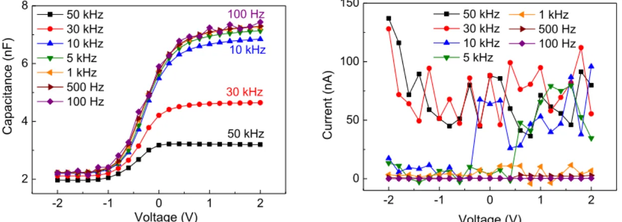
Figure 4.6. Frequency dependence of C(V) characteristics (left) and leakage current - I(V) (right) of an EIS sensor in pH 7 buffer solution...79
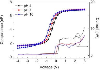
Figure 4.7. Capacitance-voltage and leakage current characteristics of Al/Si/Ta2O5 (left) and Al/Si/SiO2/Ta2O5 (right) sensors exposed to electrolytes of pH 4, 7 and 10...80
Figure 4.8 Capacitance-voltage and leakage current characteristics of Al/Si/SiO2/Ta2O5 sensor exposed to electrolytes of pH 4, 7 and 10...81
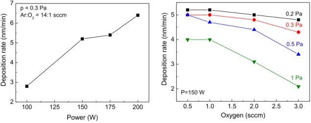
Figure 4.9. Influence of deposition parameters on the deposition rate; power (left); oxygen content and deposition pressure (right)...82
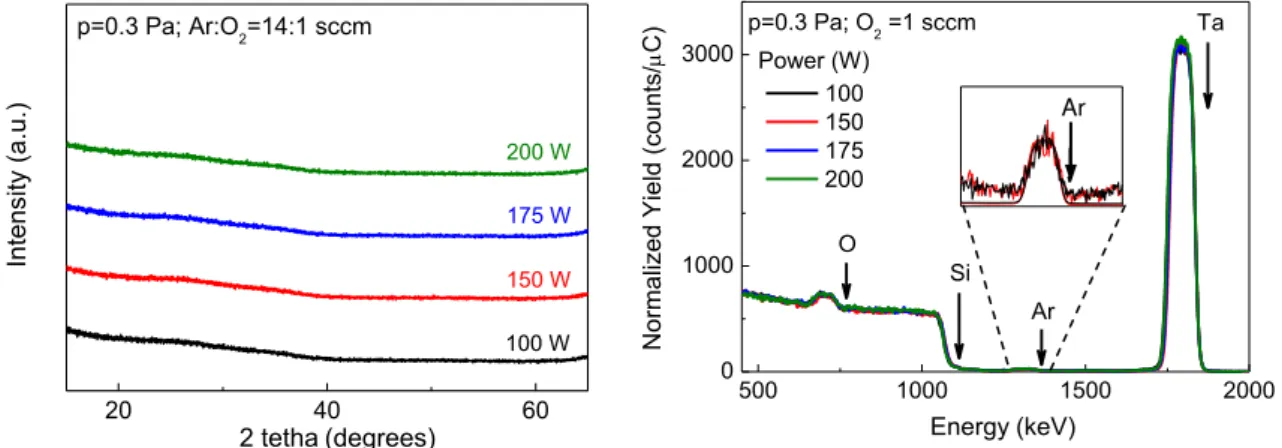
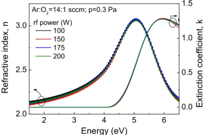
Figure 4.10. XRD diffractogram (left) and RBS spectra (right) of Ta2O5 EIS sensors produced with different rf power...83
Figure 4.11. SEM and AFM images of the Ta2O5 films deposited with 200 W rf power, Ar:O2=14:1 sccm and 0.3 Pa...84
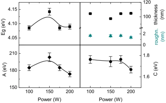
Figure 4.12. Optical transmittance spectra of Ta2O5 films deposited with varied rf power...85
Figure 4.13. Model used in spectroscopic elipsometry analysis of Ta2O5 thin films...86
Figure 4.14. Refraction index (n) and extinction coefficient (k) of Ta2O5 deposited with different rf power, obtained by modulation of SE results...86
Figure 4.15. Parameters obtained by modulation with Tauc-Lorentz dispersion of SE data of Ta2O5 deposited with different rf power...87
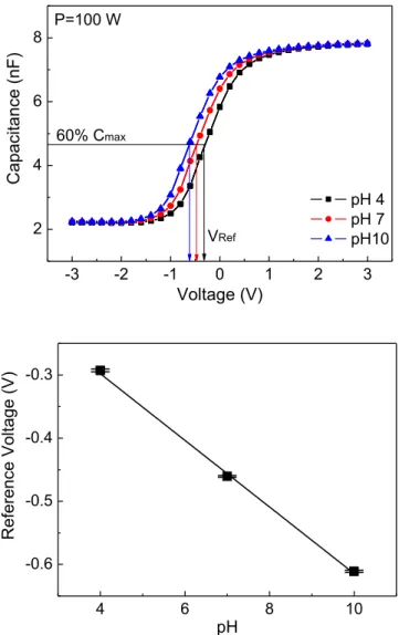
Figure 4.16. C(V) curves (top) and pH sensitivity (bottom) determination for a Ta2O5 EIS sensor produced with P=100 W, p=0.3 Pa and Ar:O2=14/1...88
xviii
Figure 4.19. RBS spectra of Ta2O5 EIS sensors produced at different deposition pressures (left) and oxygen content (right)...90
Figure 4.20. SEM (left) and AFM (right) images of the Ta2O5 films deposited with a 0.2 Pa pressure, Ar:O2=12:3 sccm and 150 W rf power...91
Figure 4.21. Parameters obtained by modulation with Tauc-Lorentz dispersion of SE data of Ta2O5 deposited with different deposition pressure and Ar:O2 ratio...92
Figure 4.22. Variation of pH sensitivity of Ta2O5 EIS sensors produced with different deposition pressure and Ar:O2 ratio...92
Figure 4.23. X-ray diffractogram of Ta2O5 film before and after post deposition annealing (vertical lines represent diffraction planes of orthorhombic Ta2O5)...94
Figure 4.24. RBS spectra of samples annealed at 200 ºC and 800 ºC with respective fit curves...94
Figure 4.25. Morphological characterization of Ta2O5 sensors: SEM micrograph and AFM deflection images (Rrms calculated using height profile) of Ta2O5 surface of sensors a) as deposited; b) annealed at 700 ºC and c) 800 ºC...95
Figure 4.26. Spectroscopic ellipsometry simulation results of the interfacial layer thickness and band-gap energy of the Ta2O5 sensors annealed at various temperatures...96
Figure 4.27. Imaginary component of the dielectric function of Ta2O5 sensors annealed at various temperatures; obtained from spectroscopic ellipsometry data modulation...97
Figure 4.28. Variation of pH sensitivity of Ta2O5 EIS sensors with post-deposition annealing temperature...97
Figure 4.29. Variation of the reference voltage obtained at 60% of maximum capacitance with annealing temperature for solution and aluminium-gated Ta2O5 EIS sensors...98
Figure 4.30. AFM image of Ta2O5 sensor after argon plasma treatment at 30 W for 10 minutes...100
Figure 4.31. Ta2O5 pH sensitivity variation with argon plasma surface treatments...101
Figure 4.32. Variation of reference voltage at pH 7 with argon plasma surface treatments...102
Figure 4.33. Ta2O5 pH sensitivity variation with oxygen plasma surface treatments...104
xix
Figure 5.2. Variation of C(V) characteristics of a penicillinase functionalized sensor when exposed to penicillin solutions of increasing concentration...111
Figure 5.3. Sensitivity of a penicillinase functionalized sensor to penicillin and its correlation with pH variation...112
Figure 5.4. Variation of C(V) characteristics of a oxygen plasma treated sensor functionalized with penicillinase when exposed to penicillin solutions of increasing concentration...114
Figure 5.5. Sensitivity to penicillin of an oxygen plasma treated sensor functionalized with penicillinase and its correlation with pH variation...115
Figure 5.6. Schematic structure of DNA molecule illustrating the chemical structure of the nucleotides, the anti-parallel nature of the two strands and the base pair hydrogen bonds that binds them together. (Becker 2009)...117
Figure 5.7. Schematic illustration of fraction of DNA molecule contained within the Debye length (D) and its variation with the ionic strength of the electrolyte (I)...120
Figure 5.8. Semi-quantitative response of EIS sensor to the presence of ssDNA and dsDNA oligonucleotides (Oligo A, Oligo B, Oligo A+B) used at different concentrations (1 and 2 µM)...124
Figure 5.9. Schematic representation of DNA amplification via PCR (Web03)...127
Figure 5.10. Conventional fluorescence-based detection with SYBR-green intercalating agent of DNA accumulation during PCR amplification. •) c-MYC gene sequence amplification, ■) PCR negative control...129
Figure 5.11. Capacitance-voltage curves obtained for a positive sample of DNA amplification at PCR cycle n (n=0, 3, 6, 9, 12, 15, 18, 21, 24, 27)...130
Figure 5.12. Field effect-based detection with optimized Ta2O5 sensitive layer of DNA
accumulation during PCR amplification. •) c-MYC gene sequence amplification, ■) PCR negative control...131
Figure 5.13. EIS sensor drift analysis: C(V) measurements performed on PCR cycle 0 following the same procedure as for the amplified DNA samples...132
Figure 5.14. Corrected data of field effect-based detection with optimized Ta2O5 sensitive layer of DNA accumulation during PCR amplification. •) c-MYC gene sequence amplification, ■) PCR negative control...132
Figure 5.15. Monitoring DNA amplification in real-time. Comparison between A) corrected Ta2O5 EIS sensor amplification curve and B) standard RT-PCR: •) c-MYC gene sequence amplification, ■) RT-PCR negative control... 134
xx
Figure 5.18. Field effect-based detection with optimized Ta2O5 sensitive layer of DNA
accumulation during LAMP DNA amplification. •) c-MYC gene sequence amplification, ■) LAMP negative control...138
Figure 5.19. EIS sensor drift analysis: C(V) measurements performed on a LAMP buffer solution following the same procedure as for the amplified DNA samples...139
Figure 6.1. Schematic representation of an extended gate amorphous oxide based ISFET...143
Figure 6.2. Amorphous oxides based extended gate ISFET sensors and detail of a TFT device...144
Figure 6.3. XRD diffractograms of semiconductor (GIZO) and multicomponent dielectric (Ta2O5:SiO2) thin films...145
Figure 6.4. RBS spectra of GIZO semiconductor (top) and multicomponent Ta2O5:SiO2 dielectric (bottom) thin films and corresponding fit lines...146
Figure 6.5. Transfer (left) and output (right) characteristics of an amorphous oxides based TFT...147
Figure 6.6. Influence of passivation on device stability and measurement reproducibility (GIZO TFT on glass/ITO/ATO substrate)...148
Figure 6.7. ISFET sensors measurement cell: real image (left) and schematic assembly representation (right)...149
Figure 6.8. Transfer characteristics obtained with VD = 0.1 V for two pH cycles (top) and pH sensitivity expressed as variation of the reference voltages with buffer solution pH (bottom)...150
Figure 6.9. Temporal response variation of the reference voltages obtained at 0.3 μA for both cycles of pH measurements...151
Figure 6.10. ISFET output characteristics at fixed gate voltage (VG = 0, 0.5, 1.0, 1.5 V) with different pH solutions...152
Figure 6.11. Device response to varied buffer solutions in a pH range between pH 2 and pH 12: (top) transfer characteristics obtained at VD = 0.1 V and (bottom) pH sensitivity expressed as variation of the reference voltages with buffer solution pH.153
Figure 6.12. Variation of the transfer characteristics of a GIZO based ITO/ATO ISFET device with buffer solution’s pH (VD = 0.1 V)...154
Figure 7.1. Image of a transparent EIS based sensor depicting peeling of the layers...165
xxi
Table 2.1. Classification of electrochemical biosensors according to type of measurement. Adapted from (Thevenot 1999)...15
Table 2.2. Overview of materials applied as sensitive layer in field effect based pH sensors...33
Table 2.3. Relevant historical milestones in the development of BioFEDs. (adapted from Schoning 2002) ...36
Table 2.4. Overview of developed EnFEDs including the enzyme used and the analyte detected. Adapted from (Dzyadevych 2006; Schoning 2002)...40
Table 3.1. Production details of each of the ISFET sensors layers. ...49
Table 4.1. Equivalent circuit parameters obtained from fitting of IS characteristics of an EIS sensor in different operation regimes...77
Table 4.2. Sputtering deposition parameters for the production of Ta2O5 EIS sensors...80
Table 4.3. Optical band gap energy of Ta2O5 films deposited with varied rf power....84
Table 4.4. Optical band gap of Ta2O5 films deposited with varied deposition pressure and Ar:O2...90
Table 4.5. Sensitivity and contact angle variation with annealing temperature. ....98
Table 4.6. Parameters obtained by modulation with Tauc-Lorentz dispersion of SE data of Ta2O5 films exposed to argon plasma under different conditions...100
Table 4.7. Parameters obtained by modulation with Tauc-Lorentz dispersion of SE data of Ta2O5 films exposed to oxygen plasma under different conditions...102
Table 5.1. Overview of penicillinase modified field effect devices for penicillin detection...108
Table 5.2. Relevant differences in Ta2O5 penicillinase FEDs produced in this worka and by Siqueira et al (2009)b...112
xxiii a.c. – alternate current
AFM – atomic force microscopy
ALD – atomic layer deposition
APTES – 3-amino-propyltriethoxysilane
ATO – aluminium oxide / titanium oxide multi-layer dielectric
AVT – average transmittance in the visible range
BioFED – biologically modified field effect device
CellFED – cell-based field effect device
CEMOP – Centre of Excellence in Microelectronics Optoelectronics and Processes
CENIMAT – Centro de Investigação de Materiais
ChemFED – chemically modified field effect device
c-Si – crystalline Si
C(V) – capacitance-voltage
CVD – chemical vapour deposition
d.c. – direct current
DNA – deoxyribonucleic acid
DNAFED – DNA field effect device
dsDNA – double stranded DNA
EG-ISFET – extended gate ion sensitive field effect transistor
EIS – electrolyte-insulator-semiconductor
EnFED – enzyme modified field effect device
FED – field effect device
FET – field effect transistor
FTO – fluorine doped tin oxide
GIZO – gallium indium zinc oxide
xxiv
ImmunoFED – immunologically modified field effect device
IPA – isopropyl alcohol
IS – impedance spectroscopy
ISFED – ion sensitive field effect device
ISFET – ion sensitive field effect transistor
ITO – indium tin oxide
IUPAC – International Union of Pure and Applied Chemistry
I(V) – current-voltage
IZO – indium zinc oxide
LAMP – loop-mediated isothermal DNA amplification
MIS – metal-insulator-semiconductor
MISFET – metal-insulator-semiconductor field-effect transistor
MOSFET – metal-oxide-semiconductor field-effect transistor
MOCVD – metal-organic chemical vapour deposition
MPCVD – microwave plasma-assisted chemical vapour deposition
nc-Diamond – nanocrystalline diamond
NIR – near infrared
NPs – nanoparticles
OHP – outer Helmholtz plane
PAMAM – polyamidoamine dendrimers
PBS – phosphate buffer solution
PCR – polymerase chain reaction
PDMS - polydimethylsiloxane
PECVD – plasma enhanced chemical vapour deposition
PenFED – penicillinase modified field effect device
PenG – penicillin G; benzylpenicillin
xxv RBS – Rutherford backscattering spectrometry
rf – radio-frequency
RT-PCR – real-time polymerase chain reaction
SAM - self-assembled monolayer
sccm – standard cubic centimeters per minute
SE – spectroscopic elipsometry
SEM – scanning electron microscopy
SNP – single nucleotide polymorphism
SPA – semiconductor parameter analyzer
ssDNA – single stranded DNA
swCNT – single-walled carbon nanotube
TCO – transparent conductive oxide
TEOS – tetraethylorthosilicate
TFT – thin-film transistor
TSO – transparent semiconductive oxide
UV – ultra-violet
Vis. – visible
W/O – without
XRD – x-ray diffraction
xxvii A – optical absorption
c – speed of light
c0– electrolyte concentration
ci– ionic concentration
C – capacitance
Cdif– differential capacitance
Cdl– double layer capacitance
CGC– Gouy-Chapman capacitance
CHelmholtz– Helmholtz capacitance
Ci– insulator capacitance
CSC– semiconductor capacitance
CStern– Stern capacitance
Ct– total capacitance
d – film thickness
dip–inter planar distance
E – energy of electromagnetic wave
EC– conduction band
EF– Fermi level
Eg - bandgap
Ei– intrinsic energy level
Eopt– optical bandgap
ERef– reference electrode potential
f – frequency
F – Faraday constant
h –Planck’s constant (4.135×10⁻¹⁵ eV.s)
xxviii ID sat– drain-to-source current in saturation regime
IG– gate leakage current
Ion– on current
Ioff– off current
Is– ionic strength
j – imaginary number
k – extinction coefficient
kB– Boltzmann constant
Ka– acid equilibrium constant
Kb– basic equilibrium constant
L – channel length
N – free carrier concentration
NA– Avogadro constant
n – refractive index
p – deposition pressure
P – rf power density
q – elementary charge of a particle (1.6×10⁻¹⁹ C)
QDNA– DNA molecule charge
Qf– fixed oxide charge
Qi– insulator charge
Qit– interface trapped oxide charge
Qm– mobile oxide charge
Qot–oxide trapped charge
Qox–oxide charge
R – reflectivity
Rrms– root-mean-square roughness
RSC– semiconductor resistance
xxix rp– parallel reflection coefficient
rs– perpendicularreflection coefficient
S – subthreshold swing
T – transmittance
TA– annealing temperature
V – voltage
VD– drain voltage
VFB– flat band voltage
VG– gate voltage
VRef– reference voltage
VT– threshold voltage
W – channel width
zi– ionic valency
Z – impedance
Z’ Zreal– real component of impedance
Z’’ Zimag– imaginary component of impedance
α – absorption coefficient
int– intrinsic buffer capacity
γLG– surface tensions of liquid−gas interface
γSG–surface tensions of solid− gas interface
γSL–surface tensions of solid−liquid interface
Δ – differential phase angle
0– vacuum permittivity
2– imaginary component of the dielectric function
el– electrolyte permittivity
i– insulator permittivity
xxx λ – wavelength of electromagnetic wave
λD– Debye length
µ –mobility
ν – frequency of electromagnetic wave
ρ – electrical resistivity
ρF– Fresnel coefficient
σ – electrical conductivity
σ0– accumulated oxide surface charge density
σd– surface charge density
χ2– error function
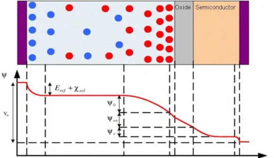
χsol– surface-dipole potential of the solution
ψ – differential amplitude angle
ψ0– oxide/electrolyte surface potential
ψS– semiconductor potential
ψox– oxide potential
– phase shift
M– metal work function
SC– semiconductor work function
1.1. Introduction ... 3
1.2. Scientific context ...5
1.3. Objectives ... 6
1.4. Thesis outline ... 7
3
Chapter 1. Motivation
1.1. Introduction
Biosensors represent a well established market involving high investments in research
and industry. The variety of sensors and sensor applications is overwhelming and still it
is expected to continue to grow. Perhaps the most recognized and successful example is
the glucose biosensor. It represents about 70 % of the biosensors market and has
become a household device for diabetes monitoring. A similar development can be
ambitioned for other sensors, including DNA diagnostics. DNA detection based
diagnostics have applications in various fields such as pathogen identification, drug
screening and diagnosis of genetic diseases. The development of sensors that allow for
fast, simple and cost-effective detection of DNA, especially for point-of-care
applications, is thus highly desirable; as demonstrated in Figure 1.1 (Drummond 2003;
McKinnon 2009; Shinwari 2007).
Figure 1.1. The total biosensors market, showing the percent of revenues predicted by vertical
markets (world) for 2016, based on 2009 market values (Web01).
Field effect devices are a promising alternative in the label free detection of DNA and
consequently considerable research efforts have been invested towards their
development. These devices provide several advantages: small dimensions, fast
response, possibility of integration into biosensor arrays and the possibility of low-cost
mass production. As such, the simultaneous analysis of various DNA targets in
miniaturised analytical systems, as lab-on-chip sensors, could become a reality
(Shinwari 2007; Schoning 2002). In fact, last year, it became a reality with the
publication ‘An integrated semiconductor device enabling non-optical genome sequencing’ in Nature (Rothberg 2011) and subsequent application of this technology to a commercially available DNA sequencing equipment – IonTorrent TM
4
The incorporation of a nucleotide into strand of DNA by a polymerase releases a
hydrogen ion as a by-product; resulting in a local pH variation that can be detected by
the underlying ISFET sensor and converted to a measurable signal. The IonTorrent is
similar to standard fluorescence-based DNA sequencing equipments that uses a
high-density array of wells, each holding a different DNA template, to perform this
biochemical process in a massively parallel way. The difference is that beneath the wells
lies an array of ion-sensitive field effect sensors, fabricated by standard CMOS
technology Figure 1.2. The ISFET directly detects the sequencing event thus eliminating
the need for fluorescent labels and complex optical detection methods and equipments.
Figure 1.2. Ion sensitive chips: a) 8′′ wafer containing 200 ion sensor die; b) unpackaged die and c) die in ceramic package with moulded fluidic lid to allow addition of sequencing reagents
5
1.2. Scientific context
Since the introduction of the ion sensitive field-effect transistor (ISFET) in the 1970’s
by Bergveld the development of these devices and their applications has significantly
grown. However, it took almost 30 years for the first pH sensitive ISFET to be
commercially available and despite the intensive research and the breakthrough of
IonTorrent TM, that testifies to the enormous possibilities of field effect based
biosensors (BioFEDs), no other BioFED device has been made commercially available.
The reality is that, together with all their advantages, FEDs also possess some
drawbacks related to device stability, reproducibility and drift issues. Low-cost
disposable sensors, which for some applications are preferred, would resolve most of
these drawbacks while presenting new challenges. The use of plastic or even paper
substrates for field effect sensor’s production would require low temperature fabrication process. This is not possible for silicon-based technology nor with the
commonly used fabrication techniques for Si based FEDs. Consequently alternative
fabrication methods and materials should be pursuit.
Field effect devices based on oxide semiconductors and materials produced by radio
frequency (rf) magnetron sputtering have demonstrated excellent properties and are
compatible with low-cost substrates due to the low process temperature (Barquinha
2010 and 2010a; Fortunato 2008 and 2008a; Pereira 2008). The remarkable
development of oxide semiconductors based devices and their application in display
technology has established these as a new generation of electronic devices, providing an
attractive alternative for BioFEDs sensors. (Barquinha 2012; Fortunato 2012)
The development of the sensitive layer for field effect based sensors will be the main
focus of this work as most of the currently reported sensitive materials are either
produced via high temperature techniques, such as thermal oxidation, or require
post-deposition annealing at high temperatures. To overcome these drawbacks and produce
a sensitive layer under conditions compatible with low-cost and/or flexible substrates,
rf magnetron sputtering was chosen as the deposition technique for it allows the
deposition of materials at low temperature.
In this context the aim of this work is the production, study and optimization of the
sensitive layer by rf magnetron sputtering and its application in field effect based
6
1.3. Objectives
The development of field effect based biosensors within the microelectronic and
optoelectronic research group was initiated by this work. As such, one of the initial
objectives was to establish the necessary conditions for the development of biosensors
research. For that the remodelling and refurbishing of a new dedicated laboratory as
well as the acquisition of specific equipments and adaptation of existing equipment, to
allow measurements with solutions, was initially performed.
The main goals of this work are:
The production and study of low temperature sputtered Ta2O5 thin films for application as a sensitive layer in field effect based sensors.
The optimization of the Ta2O5 sensitive layer production and post-production parameters, towards maximum pH sensitivity.
Production of enzyme functionalized field effect devices (EnFED) for penicillin detection.
The field effect detection of DNA and real-time label-free monitoring of DNA amplification via polymerase chain reaction (PCR) and loop-mediated isothermal
amplification (LAMP).
The low temperature production of oxide semiconductor based ISFETs comprising the optimized Ta2O5 sensitive layer and their application as field effect based
7
1.4. Thesis outline
Chapter 1 presents the aim and motivation of this study.
Chapter 2 provides some fundamental background regarding the functioning principle of field effect based devices and the electric potential of the
electrolyte/oxide interface. A brief overview of materials applied as sensitive layer
in FEDs and of BioFEDs developments is also described.
Chapter 3 describes the production and characterization techniques used during the research work of this dissertation, mostly highlighting rf magnetron sputtering
and electrochemical characterization of the devices.
Chapter 4 focuses on the presentation and discussion of the main results obtained on tantalum pentoxide thin films produced by rf magnetron sputtering
and their application as pH sensitive layer in FEDs. The influence of several
processing and post-processing parameters on the films properties and pH
sensitivity is analyzed. A section of this chapter is devoted to the establishment of
the measurement protocol as it proved to be crucial to obtain reliable data.
Chapter 5 describes the main results obtained for the detection of biomolecules. The production of enzyme functionalized field effect devices (EnFEDs) and results
for penicillin detection are presented and discussed. Also, results of the field effect
detection of DNA and real-time label-free monitoring of DNA amplification via
polymerase chain reaction (PCR) and loop-mediated isothermal amplification
(LAMP) are presented and the detection mechanism is discussed.
Chapter 6 is devoted to the presentation and discussion of the production of oxide semiconductor-based ISFETs comprising the optimized Ta2O5 sensitive layer
and their application as field effect based sensors.
8
1.5. Publications and presentations
The main results obtained during this dissertation were presented in several
international conferences and published in peer-reviewed publications.
Publications
R. Branquinho, B. Veigas, J. V. Pinto, R. Martins, E. Fortunato and P. V. Baptista, 'Real-time monitoring of PCR amplification of proto-oncogene c-MYC using a Ta2O5
electrolyte–insulator–semiconductor sensor', Biosensors and Bioelectronics, 2011,
28, p. 44-49.
R. Branquinho, J.V. Pinto, T. Busani, P. Barquinha, L. Pereira, P.V. Baptista, R. Martins, E. Fortunato, 'Biosensors based on Sputtered Ta2O5 with Low Thermal
Annealing', IEEE/OSA Journal of Display Technology Special Issue in association
with the 8th International Thin Film Transistor Conference (ITC 2012), in press.
J.V. Pinto, R. Branquinho, P. Barquinha, E. Alves, R. Martins, E. Fortunato, 'Extended-gate ISFETs based on Sputtered Amorphous Oxides', IEEE/OSA Journal
of Display Technology Special Issue in association with the 8th International Thin
Film Transistor Conference (ITC 2012), in press.
Oral presentations in international conferences
R. Branquinho*, B. Veigas, J. V. Pinto, P. Baptista, R. Martins, E. Fortunato, 'Sputtered Ta2O5 Field Effect Based Biosensors', EMRS 2011 Fall Meeting,
Warsaw, Poland, 19-23 September 2011.
J.V. Pinto*, R. Branquinho, P. Barquinha, R. Martins, E. Fortunato, 'ISFETs based on amorphous oxides and produced at room temperature', EMRS 2011 Fall
Meeting, Warsaw, Poland, 19-23 September 2011.
R. Branquinho, J.V. Pinto, L. Pereira, P. Barquinha, P. Estrela, P. Baptista, R. Martins, E. Fortunato* 'New Amorphous Oxide-based ISFETs for Biosensor
Applications' MRS2010 Spring Meeting, San Francisco USA 5-9 April 2010.
R. Branquinho*, J. V. Pinto, P. Barquinha, L. Pereira, P. Estrela, P. Baptista, R. Martins, E. Fortunato 'Room Temperature Sputtered Ta2O5 for Solid State
9
Poster presentations in international conferences
R. Branquinho*, J. V. Pinto, T. Busani, P. Barquinha, L. Pereira, P. V. Baptista, R. Martins, E. Fortunato, 'Biosensors based on Sputtered Ta2O5 with Low Thermal
Annealing', ITC 2012, Lisbon PT, 30-31 January 2012
J. V. Pinto*, R. Branquinho, P. Barquinha, E. Alves, R. Martins, E. Fortunato, 'Extended-gate ISFETs based on Sputtered Amorphous Oxides', ITC 2012, Lisbon
PT, 30-31 January 2012
R. Branquinho*, B. Veigas, J. V. Pinto, R. Martins, P.V. Baptista, E. Fortunato, 'Ta2O5 electrolyte-insulator-semiconductor sensor for Real Time PCR',
Bio-Sensing Technology 2011, Amsterdam, The Netherlands, 10-12 October 2011
J.V. Pinto, R. Branquinho*, P. Barquinha, P. Estrela, R. Martins, E. Fortunato,
‘Room Temperature Processed ISFETs Based on Amorphous Oxides’, Bio-Sensing Technology 2011, Amsterdam, The Netherlands, 10-12 October 2011
R. Branquinho*, J. V. Pinto, P. Barquinha, L. Pereira, P. Estrela, P. Baptista, R. Martins, E. Fortunato 'Room Temperature Sputtered Ta2O5 for Solid State
Biosensors' TNT2010, Braga PT 6-10 September 2010 – Best Poster Award
R. Branquinho*, J. V. Pinto, P. Barquinha, L. Pereira, P. Baptista, R. Martins, E. Fortunato 'Room temperature sputtered high-k dielectrics for biosensing
2.1. Biosensors ... 13
2.2. Field effect based sensors ... 15
2.2.1. Electrolyte-Insulator-Semiconductor (EIS) capacitors ... 15
2.2.2. Ion-Sensitive-Field-Effect-Transistors (ISFETs) ... 20
2.3. Oxide/Electrolyte interface ... 23
2.3.1. Electrochemical double layer ... 24
2.3.2. Site binding model ... 27
2.4. Sensitive layer ... 31
2.5. Field effect biosensors (BioFEDs) ... 34
2.5.1. Chemically-modified FEDs (ChemFEDs) ... 35
2.5.2. Immunologically modified FEDs (ImmunoFEDs) ... 36
2.5.3. Cell-based FEDs (CellFEDs) ... 37
2.5.4. Enzyme-modified FEDs (EnFEDs) ... 38
13
Chapter 2.
Introduction
In this chapter a fundamental background regarding the functioning principle of
biosensors, field effect based devices and the electric potential of the electrolyte/oxide
surfaces interface is provided. A brief overview of the materials applied as sensitive
layer in FEDs and of BioFEDs developments is also described.
2.1. Biosensors
As defined by IUPAC (International Union of Pure and Applied Chemistry) a chemical
sensor is a device that transforms chemical information, ranging from the
concentration of a specific sample component to total composition analysis, into an
analytically useful signal. Chemical sensors usually contain two basic components
connected in series: a chemical (molecular) recognition system (receptor) and a
physicochemical transducer. Biosensors are chemical sensors in which the recognition
system utilizes a biochemical mechanism (Thevenot 1999; Turner 1987).
The recognition system can be based on organic or inorganic materials and biologically
active substances can be proteins, enzymes, antibodies or antigens, nucleotides, whole
cells or even an insect’s sensory organ (Schoning 2002). The specificity and selectivity
is thus provided by the sensitive layer that upon interaction with a substance of interest
(analyte) generates a physical-chemical change. This change is detected and translated
by the transducer into a measurable signal that is directly correlated to the analyte
concentration. A schematic representation of a biosensor system is shown in Figure 2.1.
Figure 2.1. Generalized schematics of a biosensor system.
Biosensors should ideally demonstrate stability during operation and overtime,
reversibility of the recognition event; a linear range of operation; defined detection
14
Biosensors can be classified according to the nature of the variation that occurs from
the physical-chemical interaction between the analyte and the sensitive layer. These
can be optic, thermal, acoustic, magnetic, piezoelectric or electrochemical, to name just
a few. Electrochemical sensors, in their turn, can be divided into potentiometric,
amperometric, conductometric and field effect-based according to the measurement
type. Table 2.1 shows some examples of transducers and respective analytes from each
class of electrochemical sensors.
Table 2.1. Classification of electrochemical biosensors according to type of measurement.
Adapted from (Thevenot 1999).
Measurement Transducer Analyte
Amperometric Metal or carbon electrodes;
Chemically modified
electrodes
O2, sugars, alcohols…;
Sugars, alcohols, phenols,
oligonucleotides…
Conductometric Interdigitated electrodes;
Metal electrode
Charged species,
oligonucleotides…
Potentiometric Glass electrode;
Ion-seletive electrode
(ISE);
Gas electrode;
Metal electrode
H+, Na+;
K+, Ca2+, Cl-, F-…
CO2, NH3;
redox species
Field effect Ion-sensitive field effect
device (ISFED);
Enzyme FED (EnFED);
DNA-based FED
H+, Na+, K+, Ca2+, Cl-, F-,
charged species…
Penicillin, glucose, urea… DNA, oligonucleotides…
Historically the first biosensor was reported in 1962 (Clark and Lyons, 1962). It was an
electrochemical biosensor where an enzyme (glucose-oxidase) membrane was
combined with an oxygen electrode to yield the well known glucose sensor. The interest
and development of biosensors has been growing ever since due to the uncountable
possibilities of applications of such devices. The demands in process control and
monitoring of complex biochemical reactions both in-vitro and in-vivo and the
constant progress in biotechnology (genomics, proteomics and pharmaceuticals) have
been some of the driving forces behind the increased development of this new
15
2.2. Field effect based sensors
In field effect based biosensors the transducer is usually a
metal-insulator-semiconductor (MIS) capacitor or metal-oxide-metal-insulator-semiconductor field effect transistor
(MOSFET) that are slightly modified. Initially classified as potentiometric sensors,
since the detection mechanism is based on an electrical potential variation at the
transducer when placed in contact with an electrolyte, these were separated into a new
class of electrochemical biosensors after 30 years of their discovery; which
demonstrates their importance (Dzyadevych 2006; Thevenot 1999).
The first ion sensitive field effect transistor (ISFET) was invented by Bergveld (Figure
2.2) in the 1970’s (Bergveld 1970 and 1972) where it was applied for
electrophysiological measurements of the composition of the area surrounding nerve
tissues. It was shown that with this device not only electrical potentials but also ion
concentrations could be measured hence the name ion sensitive field effect transistor
(Bergveld 2003). The electrolyte-insulator-semiconductor (EIS) capacitor has also been
widely studied for biosensing applications.
Figure 2.2. Professor Piet Bergveld (from http://www.knaw.nl/)
The structure and operation principles of electrolyte-insulator-semiconductor (EIS)
capacitors and ion sensitive field effect transistors (ISFET) are presented in the next
sections.
2.2.1. Electrolyte-Insulator-Semiconductor (EIS) capacitors
The EIS structure, as depicted in Figure 2.3, is identical to that of a
metal-insulator-semiconductor (MIS) capacitor where the gate electrode is replaced by an electrolyte
and a reference electrode (ERef); usually Ag/AgCl. The insulator, commonly an oxide, is
thus directly exposed to the electrolyte so changes in the solution can affect the oxide
16
Figure 2.3. Schematic illustration of MIS and EIS structures. ERef: reference electrode; VG: gate voltage.
The operation principles of EIS sensors are thus similar to those of the MIS capacitor
with additional parameters arising from the additional components (electrolyte and
reference electrode).
The MIS capacitor is one of the most simple and useful devices in the study of
electronic circuits. The Si-SiO2 MIS structure was first reported in 1960 by Ligenza et al
and it is still looked upon as the most ideal semiconductor-insulator interface to serve
as a model for understanding surface physics in electronic devices. (Sze 2007)
The MIS capacitor is a two electrode device where a semiconductor is separated from
the gate electrode by an insulator layer. It is similar to a parallel plate capacitor with an
additional semiconductor layer that has a variable capacitance. By applying a voltage to
the gate electrode the space-charge distribution in the semiconductor can be
modulated. The total capacitance of the device (C) is a series combination of the
insulator capacitance (Ci) and the voltage dependent semiconductor capacitance (Csc).
( 2.1 )
For an insulator of a given thickness (d) Ci is constant, corresponding to the maximum
capacitance of the system, and depends only on the material’s properties and device
geometry (Ci=0iA/d; where 0 and i are the air and insulator permittivity respectively
and A is the surface area). The semiconductor’s capacitance is variable and is
determined by the space-charge region thickness which is dependent on the voltage
applied to the gate electrode. The capacitance-voltage characteristics of the MIS device
show three different regions depending on the applied gate voltage (VG): accumulation,
17
The capacitance-voltage characteristics of a MIS device can be obtained by applying a
dc gate voltage with a superimposed small ac signal of known frequency. A typical C-V
curve of an ideal p-type Si/SiO2 MIS capacitor is depicted in Figure 2.4.
Figure 2.4. Capacitance-voltage characteristics of an ideal p-type MIS structure. Adapted from
(Schroder 2006)
The different regimes can be explained with the energy-band diagram of an ideal MIS
structure (Figure 2.5), where it is assumed that under the biasing conditions no current
flows through the insulator and the only charges that exist are those in the gate
electrode which are mirrored in the semiconductor (equal but of opposite sign).
Figure 2.5. Energy-band diagram of an ideal p-type MIS capacitor in flat-band condition;
accumulation; depletion and inversion regimes. Adapted from (Sze 2007)
The system is in equilibrium when no voltage is applied (VG=0 V) to the device and
assuming that there is no difference between the metal gate and semiconductor work
functions, the Fermi level of the semiconductor is flat (flat-band condition) and aligned
with the metal’s Fermi level.
The device is in accumulation when a negative voltage is applied to the gate electrode
(VG<0 V). Under negative bias the silicon energy bands bend upwards and positive +VG
-VG
high frequency
low frequency
VFB
Inversion Accumulation Depletion
Capac
itanc
e
Voltage Ci
18
charges (holes); which are the majority charge carriers in p-type Si; accumulate at the
semiconductor-insulator interface creating a thin charged layer. In this accumulation
regime the device is similar to a parallel plate capacitor and the total capacitance is
defined by the insulator capacitance (C=Ci) corresponding to the maximum capacitance
of the system.
When the gate electrode is positively biased (VG>0 V) the energy band bend downwards
and the electric field pushes the positive charge carriers away from the interface, thus
forming a depletion region, that acts as an insulator, at the semiconductor-insulator
interface. The thickness of the depletion region (wd) increases with applied potential
hence the depletion layer capacitance decreases, consequently the total capacitance will
also decrease (equation ( 2.1)).
Further increase in applied voltage (VG>>0 V) causes the intrinsic level to cross over
the semiconductor Fermi level which leads to the accumulation of electrons; the
minority charge carriers in p-type Si; at the Si/SiO2 interface. When the electron
concentration exceeds the hole concentration at the interface a thin n-type layer forms
within the p-type Si, hence the designation inversion. This region of the curve can
assume two forms depending on the measuring frequency. For low frequency the
electron concentration can follow the ac signal applied so total capacitance increases
reaching maximum value close to Ci in a similar way as in accumulation. At high
frequency the electron concentration cannot follow the signal variation because it is
faster than the recombination-generation rates of these minority charge carriers. In this
case the capacitance curve reaches a plateau of minimum capacitance (Sze 2007;
Schroder 2006).
The ideal MIS structure is useful for describing and understanding the
capacitance-voltage characteristics of this type of devices however in a non-ideal capacitor other
parameters must be taken into account. In a non-ideal capacitor the flat-band voltage
(VFB) is not usually zero and its value is affected by the existence of oxide charges (such
as interface trapped charges –Qit; fixed oxide charge – Qf; mobile ionic charge –Qm;
and oxide trapped charge –Qot) and also by the work function difference between the
semiconductor (sc) and the gate metal (M).
(2.2)
In this case the system is not in equilibrium when VG =0 V and it is necessary to apply a
certain voltage to attain the flat-band condition (Figure 2.6). The experimental C-V
19
Figure 2.6. Band-diagram with VFB≠0 at VG=0 V (left) and new flat-band voltage; VG=VFB (right).
The flat-band voltage (VFB) is the most relevant parameter when considering these
devices for sensing applications because its value will be affected by the changes in
solution.
The EIS sensor is basically a MIS capacitor where the metal gate electrode is
substituted by an electrolyte and a reference electrode (Figure 2.3). The
capacitance-voltage characteristics of an EIS device can be obtained in a similar way by applying a
dc voltage though the reference electrode with a superimposed small ac signal of known
frequency.
The expressions obtained for the MIS device can be modified to account for the
additional potential contributions from the reference electrode and electrolyte.
The flat-band voltage of an EIS sensor can thus be expressed as:
(2.3)
where ERef is the reference electrode potential, sol is the surface-dipole potential of the
solution, which are constant for a given solution; and 0 is the electrolyte/insulator
interface potential, which is determined by the interaction of ions in solution with
insulator active surface sites (Barabash 1987; Bergveld 2003). Depending on the ion
concentration the insulator surface potential will change so the space-charge
capacitance, and consequently the total capacitance, is thus modulated by the
electrolyte composition.
Similarly to the MIS device and for controlled electrolyte concentration and
measurement frequency, the capacitance-voltage characteristics of the EIS sensor can
be described by a series combination of the insulator capacitance and the space-charge
capacitance. However the space-charge capacitance can be modulated by electrolyte
composition through variations in the electrolyte/insulator surface potential (Bousse
20
The electrochemical potential of ionic species in solution and the electrolyte/insulator
surface potential (0) will be discussed in more detail in section 2.3.
2.2.2. Ion-Sensitive-Field-Effect-Transistors (ISFETs)
As described in the previous section for the EIS sensor, the ISFET sensor structure and
operation can be related to its electronic counterpart; the field effect transistor (FET).
Again by replacing the gate electrode with an electrolyte and a reference electrode the
gate dielectric, typically an oxide, is directly exposed to the electrolyte so changes in the
solution can affect the oxide surface potential and modulate the device’s response. A
schematic representation of a FET and an ISFET structure is depicted in Figure 2.7.
Figure 2.7. Schematic structure of FET and ISFET.
The field effect transistor is one of the most important electronic devices in integrated
circuits such as microprocessors and memories. Its invention was patented in the 1930s
by Lilienfeld but due to the lack of adequate materials and technological facilities its
successful fabrication was only reported 23 years later by Shockley. In the 1960s the
production of the Si-SiO2 based MOSFET and the thin film transistor (TFT) led to the
increased interest and development of these devices. Although MOSFETs and TFTs
differ in some aspects (mainly in the materials properties, modes of conduction,
fabrication process and device substrate) the operation principle is the same (Sze 2006;
Tickle 1969).
The field effect transistor can be generically described as a three electrode device where
the current flow between the source and drain electrodes (ID) can be modulated by
21
layer is separated from the gate electrode by an insulator layer that prevents current
flow between them. In this way the FET gate structure is similar to a MIS capacitor so
the field effect modulation of charge carrier’s concentration at the
semiconductor-insulator interface can be explained by the energy band diagram variation of this
capacitor with applied VG. Figure 2.8 depicts the energy bands diagram of an ideal
capacitor comprising an n-type semiconductor.
Figure 2.8. Energy band diagrams of an ideal gate electrode/dielectric/n-type semiconductor
capacitor for different bias conditions: (a) equilibrium (VG=0 V); (b) depletion (VG<0 V); (c)
accumulation (VG>0 V).
As explained in the previous section for p-type Si, band bending occurs when a voltage
is applied to the gate electrode however for n-type semiconductors the polarity is
reversed because in this case the majority charge carriers are electrons. When the gate
electrode is negatively biased (VG<0 V) electrons are repelled from the
semiconductor-insulator interface creating a depletion layer that acts as an semiconductor-insulator, consequently
negligible current flows between source and drain (ID) even at high drain-source
voltage (VD). Accumulation occurs when a positive bias, which attracts electrons to the
semiconductor surface, is applied to the gate (VG>0 V). A conductive channel forms at
the semiconductor-insulator interface when a sufficiently high concentration of
electrons is accumulated in this region and current can flow between source and drain
(ID>0 A). The conduction mechanism differs from silicon because in this case no
inversion layer is formed. (Sze 2006, Tickle 1969)
The voltage required to generate the conductive channel is the threshold voltage (VT).
At voltages higher than the threshold, the accumulation charges increases which leads
to an increase in the channel conductance and in drain-source current flow (ID). The
gate voltage thus modulates the channel conductance and, as it is increased, the TFT