Licenciado em Ciências da Engenharia Electrotécnica e de Computadores
Wideband CMOS Receiver
Dissertação para obtenção do Grau de Mestre em Engenharia Electrotécnica e de Computadores
Orientador :
Prof. Dr. Luís Augusto Bica Gomes de Oliveira,
Prof. Auxiliar, Universidade Nova de Lisboa
Júri:
Presidente: Prof. Dr. Rui Manuel Leitão Santos Tavares
Arguente: Prof. Dr. Rui Miguel Henriques Dias Morgado Dinis
Wideband CMOS Receiver
Copyright c Miguel Duarte Madeira Fernandes, Faculdade de Ciências e Tecnologia,
Universidade Nova de Lisboa
Acknowledgements
Antes de mais, gostaria de agradecer ao Departamento de Eng. Electrotécnica e à Facul-dade de Ciências e Tecnologias da UniversiFacul-dade Nova de Lisboa pela oportuniFacul-dade que me deram de crescer como pessoa e como engenheiro ao longo dos últimos seis anos. Certamente o que aprendi, nas aulas e fora delas, será bastante útil para o meu futuro. Nunca esquecerei os momentos de convívio que me foram proporcionados e as pessoas que tive a felicidade de conhecer.
Não poderia deixar de agradecer ao meu professor e orientador, Prof. Luís Oliveira, por todo o apoio e ajuda que me deu ao longo deste ano, e por sempre ter acreditado em mim e nas minhas capacidades. Gostava também de agradecer aos restantes profes-sores da secção de Electrónica que me foram dando o seu apoio ao longo da dissertação, especialmente ao professor João Oliveira e ao professor João Goes.
Um especial obrigado ao Daniel Marques, João Almeida, Miguel Taborda, Pedro Car-rasco e Diogo Barata pela companhia que me fizeram ao longo do curso, pelos dias de estudo no Skype e por os momentos de diversão que me proporcionaram ao longo destes últimos anos. Não esquecendo os meus colegas do gabinete 3.5 que me apoiaram e me foram ajudando ao longo deste último ano. Deixo ainda um especial agradecimento ao Gonçalo Lourenço pela companhia que me fez durante o desenvolvimento e escrita da tese, pelos almoços (que não pagou) e pelas tardes bem passadas na esplanada.
Quero ainda agradecer à minha família, principalmente aos meus pais e aos meus avós, por todo o suporte que me deram ao longo destes anos de ensino, pela liberdade que sempre me deram para poder seguir os meus sonhos e obviamente por me terem pago os estudos e terem apoiado sempre as minhas decisões. Certamente sem eles não seria possível chegar onde estou hoje. Agradeço ainda ao meu irmão, João Fernandes, por todas as distracções que me foi dando ao longo do curso, que me obrigaram a ficar a estudar até mais tarde do que queria para compensar, e também pela ajuda que me deu nalgumas disciplinas.
que me proporcionou ao longo deste último ano. Certamente sem a sua contribuição tudo teria sido muito mais complicado.
Abstract
In this thesis a wideband radio frequency (RF) receiver, with integrated filtering that can be precisely controlled by the local oscillator (LO) frequency to attenuate out-of-band interferers, is presented. Two key blocks of the receiver are studied: low-noise amplifier (LNA) and mixer. The LNA consists in a widely tunable narrowband balun-LNA with integrated high-Q bandpass filters (BPF), which allows the attenuation of undesired in-terferers that can corrupt the desired signal. The mixer is a passive current-driven circuit that also performs filtering, due to its impedance transformation properties. For the LNA, developed in 130 nm, simulation results show a voltage gain higher than23.8dB, a noise figure (NF) lower than3.3dB, anIIP2 >22dBm and anIIP3 >−4dBm, for a working band between0.3GHz and1GHz with a power consumption of3.6mW. Regarding the
receiver analog front-end (AFE) it was obtained a NF lower than10dB, for intermediate frequencies (IF) of interest, and anIIP3of0.23dBm.
To convert the IF signal at the mixer’s output to the digital domain a current-mode sigma-delta (Σ∆) modulator is employed. Since theΣ∆was implemented using CMOS 65 nm technology, the studied receiver was redesigned in this technology to allow the full integration of the receiver. Operating at full scale, theΣ∆modulator shows aSN DR = 36.9dB and anEN OB= 6.2bits.
Keywords: High-Q BPF, N-path filter, widely tunable LNA, SAW-less receiver,
Resumo
Neste trabalho foi desenvolvido um recetor de rádio frequência (RF) de banda larga, com filtros integrados que podem ser sintonizados através da frequência do oscilador, para atenuar interferentes indesejados. Foram estudados dois blocos cruciais do recetor: low-noise amplifier(LNA) e misturador. O LNA consiste num balun-LNA de banda es-treita com filtros integrados, que permite a atenuação de sinais interferentes que podem corromper o sinal desejado. O misturador consiste num circuito passivo que funciona em modo de corrente e que, devido às suas propriedades de transformação de impedâncias, também atua como filtro. Relativamente ao LNA, desenvolvido em CMOS 130 nm, foi obtido um ganho de tensão maior do que23.8 dB, umanoise figure(NF) menor do que 3.3 dB, umIIP2 > 22dBm e um IIP3 > −4dBm, para uma banda de funcionamento entre0.3 GHz e1GHz e um consumo de potência de3.6mW. Relativamente aoanalog front-end(AFE) do recetor foi obtida uma NF menor do que10 dB, para as frequências
intermédias (IF) de interesse, e umIIP3igual a0.23dBm.
Para converter o sinal à saída do misturador para o domínio digital foi utilizado um moduladorΣ∆ que funciona em modo de corrente. Como o Σ∆ foi desenvolvido em
CMOS 65 nm foi necessário redesenhar o recetor nesta tecnologia para ser possível obter um recetor completamente integrado no mesmo chip. À saída do Σ∆ foi obtido um
SN DR= 36.9dB e umEN OB= 6.2bits, a operar emfull-scale.
Palavras-chave: Filtros passa-banda com elevado Q, filtros N-path, LNA sintonizável,
Contents
Acknowledgements vii
Abstract ix
Resumo xi
Acronyms xxiii
1 Introduction 1
1.1 Background and Motivation . . . 1
1.2 Thesis Organization . . . 2
1.3 Main Contributions . . . 3
2 Receiver Architectures and RF Blocks 5 2.1 Basic Concepts . . . 5
2.1.1 Impedance Matching . . . 5
2.1.2 Scattering Parameters . . . 8
2.1.3 Gain . . . 9
2.1.4 Noise . . . 10
2.1.4.1 Thermal Noise . . . 10
2.1.4.2 Flicker Noise . . . 11
2.1.4.3 Noise Figure . . . 12
2.1.5 Nonlinearities Effects . . . 13
2.1.5.1 Gain Compression . . . 14
2.1.5.2 Intermodulation Distortion . . . 15
2.2 Receiver Architectures . . . 17
2.2.1 Heterodyne Receiver . . . 17
2.2.2 Homodyne Receiver . . . 18
2.2.3 Low-IF Receiver . . . 20
2.3.1 Narrowband LNAs . . . 22
2.3.1.1 Common-Source LNA with Inductive Degeneration . . . 22
2.3.2 Wideband LNAs . . . 23
2.3.2.1 Common-Source with Resistive Input Matching . . . 23
2.3.2.2 Common-Gate . . . 24
2.3.3 Discussion . . . 25
2.4 Mixers . . . 25
2.4.1 Performance Parameters . . . 26
2.4.2 Passive Mixers . . . 27
2.4.3 Active Mixers . . . 29
2.4.4 Discussion . . . 30
2.5 RF Filters . . . 31
2.6 Analog-to-Digital Converters . . . 32
3 Wideband Cascode Balun-LNA 35 3.1 Theoretical Analysis . . . 35
3.1.1 Input Impedance . . . 37
3.1.2 Voltage Gain . . . 37
3.1.3 Noise Factor . . . 38
3.1.3.1 Common-Gate Stage . . . 38
3.1.3.2 Common-Source Stage . . . 40
3.1.3.3 Complete LNA . . . 42
3.1.4 Load Transistors Resistance . . . 43
3.2 Circuit Implementation using CMOS 130 nm . . . 44
3.3 Circuit Implementation using CMOS 65 nm . . . 48
3.4 Discussion . . . 50
4 High-Q Bandpass Filter 53 4.1 Theoretical Analysis . . . 54
4.1.1 Single-ended Version . . . 56
4.1.2 Differential Version . . . 57
4.2 Circuit Implementation . . . 59
4.3 Discussion . . . 61
5 Complete Receiver 63 5.1 Balun-LNA with Integrated Filtering . . . 64
5.1.1 LNA With Integrated Filtering using CMOS 130 nm . . . 64
5.1.1.1 LNA Response Analysis . . . 65
5.1.1.2 LNA Frequency Sweep . . . 66
5.1.2 LNA With Integrated Filtering using CMOS 65 nm . . . 69
5.1.3 LNAs Comparison . . . 72
5.3 Complete receiver with Transimpedance Amplifier . . . 76
5.4 Current-buffer . . . 79
5.4.1 Theoretical Analysis . . . 80
5.4.2 Simulation Results . . . 81
5.5 Complete receiver with Sigma-Delta Modulator . . . 82
6 Conclusions and Future Work 85 6.1 Conclusions . . . 85
6.2 Future Work . . . 87
List of Figures
2.1 Transmission line equivalent circuit representation (adopted from [13]) . . 6
2.2 Transmission line terminated in an arbitrary load impedanceZL . . . 7
2.3 Incident and reflected waves in a two-port network . . . 8
2.4 Thevenin and Norton models of resistor thermal noise . . . 10
2.5 Thermal channel noise of a MOS transistor model . . . 11
2.6 Power spectrum of flicker and thermal noise . . . 12
2.7 Noisy two-port network . . . 13
2.8 Definition ofP1dB . . . 15
2.9 Output spectrum of IM2 and IM3 . . . 16
2.10 Definition ofIP3 . . . 16
2.11 Super-Heterdoyne receiver architecture (adopted from [3]) . . . 17
2.12 Image rejection in super-heterdoyne receiver (adopted from [3]) . . . 18
2.13 Homodyne receiver architecture (adopted from [3]) . . . 19
2.14 Homodyne receiver LO leakage (adopted from [1]) . . . 19
2.15 Effect of even-order distortion (adopted from [1]) . . . 20
2.16 Image rejection architectures: (a) Hartley (b) Weaver (adopted from [3]) . 21 2.17 CS LNA with inductive degeneration . . . 23
2.18 CS LNA with resistive input matching . . . 23
2.19 CG LNA . . . 24
2.20 Down-conversion mixer . . . 25
2.21 Mixer using a MOS switch . . . 27
2.22 Single-balanced passive mixer using a MOS switch . . . 28
2.23 (a) Current-driven passive mixer, (b) input spectrum . . . 28
2.24 Single-balanced active mixer (adopted from [3]) . . . 29
2.25 Double-balanced active mixer (adopted from [3]) . . . 30
2.26 Receiver AFE input . . . 31
2.27 BPF frequency response and Q factor . . . 32
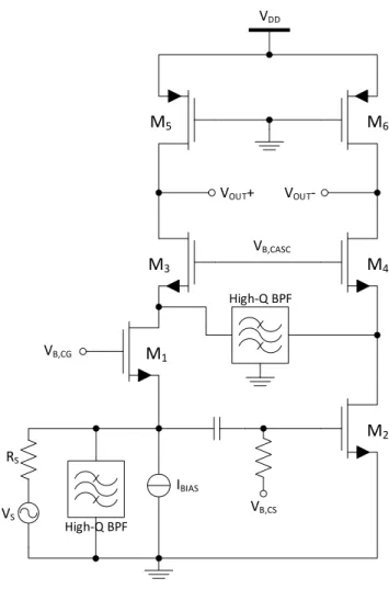
3.1 Wideband cascoded balun LNA with CG noise cancellation . . . 36
3.2 Small signal noise model of the CG stage . . . 39
3.3 CG Thevenin’s equivalent circuit . . . 40
3.4 Small signal noise model of the CS stage . . . 41
3.5 LNA input impedance . . . 46
3.6 LNAS11parameter . . . 47
3.7 LNA voltage gain . . . 47
3.8 LNA noise figure . . . 48
3.9 LNAIIP2 . . . 49
3.10 LNAIIP3 . . . 49
4.1 LPF to BPF transformation . . . 53
4.2 (a) Single-ended N-phase High-Q BPF. (b) LO waveforms for a N-phase filter 54 4.3 Single-ended M-phase high-Q BPF input impedance spectrum . . . 55
4.4 Equivalent circuit of LNA input connected to the proposed high-Q BPF . . 56
4.5 Differential N-phase High-Q BPF . . . 58
4.6 Differential M-phase high-Q BPF input impedance spectrum . . . 58
4.7 Differential N-phase High-Q BPF with floating impedances . . . 59
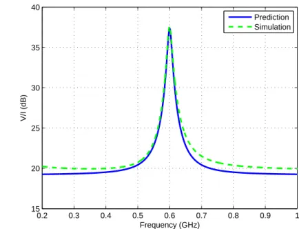
4.8 Prediction of (4.6)vs.simulation results for single-ended BPF . . . 59
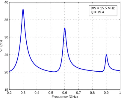
4.9 Single-ended BPF response withfLO = 300MHz . . . 60
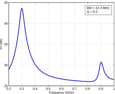
4.10 Differential BPF response withfLO= 300MHz . . . 61
5.1 Complete receiver . . . 63
5.2 Cascode balun-LNA with integrated filters . . . 65
5.3 LNA voltage gain, for multiple values of fLO, with both filters (CMOS 130nm) . . . 66
5.4 LNA noise figure, for multiple values offLO, with both filters . . . 67
5.5 LNA voltage gain atfLO . . . 67
5.6 LNA NF atfLO . . . 68
5.7 LNAS11atfLO . . . 69
5.8 LNAIIP2 andIIP3 . . . 70
5.9 LNA voltage gain, for multiple values offLO, with both filters (CMOS 65 nm) . . . 71
5.10 Mixer and TIA schematic . . . 73
5.11 Mixer input impedance withfLO = 600MHz . . . 74
5.12 TIA output signal . . . 74
5.13 Mixer NF withfLO = 1GHz . . . 75
5.14 MixerIIP3withfLO= 1GHz . . . 76
5.15 RF receiver with TIA . . . 76
5.16 Receiver output signal with one sine wave at the input . . . 77
5.18 Receiver output signal with two sine waves (a) time domain (b) DFT . . . 78
5.19 ReceiverIIP3 . . . 79
5.20 RF receiver schematic with CB andΣ∆ . . . 79
5.21 Current-buffer schematic . . . 80
5.22 Current-buffer time response . . . 82
5.23 Output spectrum of theΣ∆modulator fed by an ideal current source . . . 83
List of Tables
2.1 Comparison between Narrowband and Wideband LNAs . . . 25
3.1 LNA parameters (CMOS 130 nm) . . . 45
3.2 LNA parameters (CMOS 65 nm) . . . 50
3.3 LNA simulation results (CMOS 65 nm) . . . 50
3.4 LNA simulation results . . . 51
4.1 Single-ended high-Q BPF results . . . 60
5.1 Filters’ component values (CMOS 130 nm) . . . 64
5.2 Filtered LNA bandwidths and Q factors (CMOS 130 nm) . . . 66
5.3 LNA out-of-band voltage gain . . . 68
5.4 Filters component values (CMOS 65 nm) . . . 70
5.5 Filtered LNA bandwidth and Q factor (CMOS 65 nm) . . . 71
5.6 Narrowband balun-LNA simulation results (CMOS 65 nm) . . . 71
5.7 Filtered LNAs comparison . . . 72
5.8 Mixer parameters . . . 76
5.9 Current-buffer parameters . . . 81
Acronyms
ADC Analog-to-Digital Converter AFE Analog Front-end
BOM Bill of Materials BPF Bandpass Filter CB Current-Buffer CG Common-Gate CS Common-Source
DFT Discrete Fourier Transform FFT Fast Fourier Transform
GSM Global System for Mobile Communications HPF Highpass Filter
IC Integrated Circuit IF Intermediate Frequency IM Intermodulation
IP2 Second-order Intercept Point
IP3 Third-order Intercept Point
LO Local Oscillator LPF Low-pass Filter NF Noise Figure
P1dB 1 dB Compression Point
PSD Power Spectral Density
QAM Quadrature Amplitude Modulation RF Radio Frequency
Σ∆ Sigma-delta
SNDR Signal-to-noise and Distortion Ratio SNR Signal-to-noise Ratio
SoC System on Chip
1
Introduction
1.1
Background and Motivation
With the evolution of wireless communications, the use of wireless devices had an huge increase in the last years. These kind of communications avoids the need of a physical connection between the multiple devices, reducing the overall system costs and area oc-cupation, which is an huge advantage comparing with traditional (wired) systems. Due to these systems’ popularity there is a large interest in create compact, functional and low power devices with low cost. Contrary to other technologies, the CMOS (Comple-mentary Metal–Oxide–Semiconductor) technology allows the development of low cost and low power circuits that can operate at high frequencies. It also enables the circuit full integration in the same die (System on Chip (SoC)), avoiding the need to match the various Radio Frequency (RF) circuits’ inputs and outputs, to allow the maximum power transfer between them, and the parasitic effects due to off-chip electrical connections at high frequencies [1, 2].
wideband LNAs support multiple frequencies but have, typically, a large NF and need to guarantee the proper impedance matching over the entire working band. These kind of LNAs can also be achieved by using multiple narrowband LNAs, with very low NF, but that occupy a large area and have high power consumption. More recently, wideband LNAs that employ noise and distortion canceling techniques [4, 5] have been proposed, which can have NFs below3dB and occupy a small area.
The mixers are divided in two main groups: actives and passives. Active mixers can provide gain, reducing the overall receiver NF, but have an high power consumption and occupy a large die area. Passive mixers do not provide gain but are very small and low power. Recently, current-driven passive mixers have become very popular due to their high linearity, low noise and interesting impedance transformation properties [1]. These kind of mixers require a Transimpedance Amplifier (TIA) at the output, to convert the Intermediate Frequency (IF) signal to a voltage signal that can be processed by a typical Analog-to-Digital Converter (ADC). However, a new sort of ADCs has been emerging [6], that allows to convert a current signal directly to the digital domain, avoiding the use of a TIA that occupies die area and add more noise to the receiver.
In order to minimize interferers that can corrupt the desired receiver’s input signal, mainly by saturating the LNA, new filtering techniques [7–10], based in current-driven mixers, have been recently employed. Since these filters are passive, they can be easily integrated in the receiver, avoiding the use of external filters that occupy a large area and have an high cost.
The main goal of this work is to design a complete wideband RF receiver Analog Front-end (AFE) (except the LO) that employs the previously mentioned filtering tech-niques to attenuate interferers that can affect negatively the overall circuit performance. Also, to avoid the use of a TIA at the output of the current-driven mixer, a current-mode Sigma-delta (Σ∆) modulator [6] is used to directly convert the IF signal to the digital
domain. The receiver blocks were employed in CMOS 130 nm and CMOS 65 nm.
1.2
Thesis Organization
This thesis is organized in six chapters, including this introduction, as follows:
Chapter 2 – Receiver Architectures and RF Blocks
This chapter introduces some basic concepts and definitions that are usually employed in a RF receiver. It also reviews the key receiver architectures, including the low-IF, which is used in this work, and presents an overview of the studied receiver blocks (LNA, mixer, filters and ADC).
Chapter 3 – Wideband Cascode Balun-LNA
distortion canceling techniques that allows to reduce its noise contributions. Also, to in-crease the voltage gain and reduce the NF, the traditional load resistors are replaced by active devices. The main purpose of the cascode stages is to allow the integration of a filter, studied in chapter 4, in the LNA nodes. First, all the theoretical expressions (input impedance, load impedance, voltage gain and noise factor) of the LNA are derived and then the circuit is simulated using both CMOS 130 nm and CMOS 65 nm technologies. Finally, both technologies are compared.
Chapter 4 – High-Q Bandpass Filter
In this chapter a high-Q Bandpass Filter (BPF), based in a current-driven passive mixer, is reviewed. This filter performs impedance transformation that allows to shift a baseband impedance to the input node, transforming a low-Q Low-pass Filter (LPF) in a high-Q BPF. The circuit is intended to be used at the LNA nodes, to attenuate interferers that are located outside of the input signals band. This filter is developed in two versions, single-ended and differential, that will be employed according to the LNA nodes char-acteristics. First, the filter theoretical expressions are analyzed in order to understand its behavior and then the circuits are simulated in order to validate the obtained equations. Finally, some considerations about its functioning are made.
Chapter 5 – Complete Receiver
In this chapter the full RF receiver is presented. The LNA with integrated filtering is simulated and compared with the LNA of chapter 3, to understand the advantages and disadvantages of this technique. This analysis is made for CMOS 130 nm and CMOS 65 nm. The current-driven passive mixer, that also has filtering properties, is studied and then integrated in the full receiver, developed in 130 nm, with an ideal TIA block con-nected to the mixer’s output. To avoid the use of a TIA, a new receiver architecture is presented, employed in 65 nm. This receiver has a current-mode Σ∆ modulator
con-nected to the mixer’s output, to perform the conversion of the IF signal directly to the digital domain. The interface between the mixer and theΣ∆is made through a Current-Buffer (CB) that allows to amplify/attenuate the IF signal so that theΣ∆can operate at
maximum performance. All the circuits are validated through simulation.
Chapter 6 – Conclusions and Future Work
Finally, this chapter discusses the obtain results and presents further research sugges-tions.
1.3
Main Contributions
frequency. To achieve the desired interferers attenuation, it was designed a widely tun-able narrowband balun-LNA with integrated filtering that consists in the LNA and the high-Q BPF of chapters 3 and 4, respectively, avoiding the use of external filters that in-crease the overall circuit cost and area. To convert the desired signal to the digital domain a current-modeΣ∆modulator is used. The main advantages of this receiver are the
in-terferers attenuation, the reduced number of AFE blocks and its easy integration in the same chip.
2
Receiver Architectures and RF Blocks
The main purpose of this chapter is to introduce basic concepts related with RF electronics and to do an overview of receiver architectures and the RF front-end key blocks.
First, the basic concepts are introduced and the advantages and disadvantages of the different receiver architectures are described. Then, the basic aspects of LNAs, filters, mixers and ADCs are reviewed in order to understand their importance and how they can be integrated in a receiver AFE.
2.1
Basic Concepts
2.1.1 Impedance Matching
i(z,t)
v(z,t)
RΔz LΔz
GΔz CΔz v(z+Δz,t) i(z+Δz,t)
Δz
Figure 2.1: Transmission line equivalent circuit representation (adopted from [13])
Applying the Kirchhoff’s Voltage Law (KVL) to the circuit of Figure 2.1, and using cosine-based phasor notation for simplicity (considering steady-state sinusoidal regime), is possible to conclude that
V (z) = (R+jωL)I(z) ∆z+V (z+ ∆z) (2.1) and Kirchhoff’s Current Law (KCL) leads to
I(z) = (G+jωC)V (z+ ∆z) ∆z+I(z+ ∆z). (2.2)
Dividing the equations (2.1) and (2.2) by∆zand taking the limit as∆z→0results in the
following differential equations:
dV(z)
dz =−(R+jωL)I(z) (2.3) dI(z)
dz =−(G+jωC)V(z) (2.4)
Deriving the both terms of (2.3) and (2.4), the wave equations forV(z)andI(z)are given as follows:
d2V(z)
dz2 −γ
2V(z) = 0 (2.5)
d2I(z)
dz2 −γ
2I(z) = 0, (2.6)
where
γ=p(R+jωL)(G+jωC) (2.7)
is the complex propagation constant, which is frequency dependent. The solutions to these equations are two exponential functions for the voltage and for the current that are general solutions for transmission lines aligned along the z-axis, as shown in Figure 2.1, at a specific pointz[13]:
I(z) =Io+e−γz+Io−eγz, (2.9)
whereV+
o andIo+ are, respectively, the voltage and current amplitudes of the incident
waves andVo− and Io− are the voltage and current amplitudes of the reflected waves.
The terme−γz represents the wave propagation in the+zdirection and theeγzin the−z
direction. Deriving (2.3) and applying to (2.8), the current on the line is given by
I(z) = γ
R+jωL V
+
o e−γz−Vo−eγz
. (2.10)
Comparing the previous equation with (2.9) shows that the transmission line character-istic impedanceZ0can be defined as
Z0 = V
+
o
Io+
=−V − o
Io−
= R+jωL
γ =
s
R+jωL
G+jωC. (2.11)
Assuming an arbitrary load impedanceZL located atz = 0, as shown in Figure 2.2,
and that an incident waveform is generated from a source atz <0, from (2.8) and (2.10)
is possible to defineZLas
ZL=
V(0)
I(0) =
V+
o +Vo−
Vo+−Vo−
Z0. (2.12)
Solving the previous equation in order toV−
o /Vo+shows that the voltage reflection
coeffi-cientΓ, which is the amplitude of the reflected voltage wave normalized to the amplitude
of the incident voltage wave, is given by
Γ = V
− o
Vo+
= ZL−Z0
ZL+Z0
. (2.13)
Z
LV
+o e-γz
V
-o eγzZ
00
Γ
0z
Figure 2.2: Transmission line terminated in an arbitrary load impedanceZL
Since the time-average power that flows along a transmission line is given by [13]
Pavg =
1 2
|Vo+|2 Z0
to achieve the maximum power transfer to the load there should not exist reflected wave in order toΓ = 0, so the load impedance must be matched to the characteristic impedance
of the transmission line (ZL = Z0), as stated in 2.13. RF antennas usually have a char-acteristic impedance of 50Ωso the first block of a receiver AFE (commonly a LNA) im-plemented in an Integrated Circuit (IC) must have its input impedance matched to 50Ω.
This match can be achieved using the transistors transcondutance, as it will be shown further later, or using reactive elements that are problematic due to area consumption and bandwidth limitation. The internal blocks do not need to be matched because the distance between the blocks is so tiny that the electromagnetic wavelength is bigger than the circuit dimensions.
2.1.2 Scattering Parameters
Due to the difficulties measuring voltage and current in a RF circuit, since these mea-surements usually involve the magnitude and phase of traveling or standing waves, the circuit measurements are made using the average power instead of the traditional open-circuit or short-open-circuit measurements [12]. The scattering parameters (S-parameters) are parameters that can be obtained through those power measurements in order to describe the network. Considering a two-port network, as shown in Figure 2.3, with the the input and output incident wavesV1+andV2+, and the corresponding reflected wavesV1−and V2−, the input and output reflected waves voltage is given by [1]
V1−=S11V1++S12V2+ (2.15)
V2−=S21V1++S22V2+, (2.16) whereSmnare the different S-parameters.
Two-Port
Network
V1
V1
V2
V2
Figure 2.3: Incident and reflected waves in a two-port network
• S11is the input reflection coefficient and represents the accuracy of the input match-ing. This parameter is the ratio of the reflected and incident waves at the input port when there is no incident wave at the output port:
S11=
V1− V1+|V+
If the input of the network is completely adapted there is no reflect wave at the input (V1−) and consequentlyS11= 0. Usually aS11<−10dB means that the input of the circuit is correctly matched.
• S12 is known as reverse voltage gain and characterizes the “reverse isolation” of the circuit. This parameter is the ratio of the reflected wave at the input port to the incident wave into the output port when the input port is matched:
S12=
V1− V2+|V+
1 =0
• S21is the forward voltage gain of the network and represents the voltage gain of the circuit, as expected. This parameter is the ratio between the reflected wave at the output port and the incident wave at the input port, when the incident wave at the output is zero:
S21=
V2− V1+|V+
2 =0
• S22 is the output reflection coefficient and represents the accuracy of the output matching. This parameter is the ratio of the reflected and incident waves at the output port when there is no incident wave at the input port:
S22=
V2− V2+|V+
1 =0
Those values depend of the working frequency of the circuit and are usually repre-sented in units of dB.
2.1.3 Gain
Nowadays the signals at the input of receivers are very weak, commonly in the microvolt (µV) range, so they need to be amplified in order to allow their processing by the receiver
circuit. This factor makes the gain a very important measure of the performance of an amplifier or a mixer because it expresses the capability of the circuit to increase the am-plitude of an input signal, ideally introducing no distortion [14]. Usually there are three different types of gain considered in electronics: voltage gain, current gain and power gain. For example, the voltage gain is defined as
Av =
vout
vin
. (2.17)
If Av > 1 the input signal is amplified and if Av < 1 the input signal is attenuated.
For simplicity, the gain is often expressed in dB. It is important to note that voltage and current gains are expressed asAv,i|dB = 20 log|Av,i|and power gain is expressed
2.1.4 Noise
Noise is a random process, i.e. its instant value cannot be predicted at any time, that is present in all electronic circuits due to external interference or physical phenomena related with the nature of materials. Since the noise presence is inevitable and it degrades the circuit behavior,it is important to analyze its impact, through statistical models, and create methods that allow the minimization of its effect in the circuit [2]. In this section the two main noise sources present in CMOS transistors, thermal and flicker noise, are described. Finally NF will be presented, which is the most common measure of the noise generated by a circuit.
2.1.4.1 Thermal Noise
The thermal noise in circuits is due to thermal excitation of charge carriers in a conductor. It occurs in all resistors (including semiconductors) working above absolute zero temper-ature and introduces fluctuations in the voltage measured across the device. This kind of noise has a white (flat) spectrum that is proportional to absolute temperature [15]. In a resistor the thermal noise can be modeled as a voltage source with a Power Spectral Density (PSD) ofV2
n in series with a noiseless resistor (Thevenin equivalent), or as a
cur-rent source with a PSD ofI2
nin parallel with the same resistor (Norton equivalent) [1], as
shown in Figure 2.4. The average thermal noise power generated in a resistor is given by
V2
n = 4kT R∆f, (2.18)
wherekis the Boltzmann constant,Tis the material temperature in Kelvin and∆f is the
system bandwidth. Usually it is assumed∆f = 1, for notation simplicity, which means
that the noise power is expressed per unit bandwidth.
*
R
R
Figure 2.4: Thevenin and Norton models of resistor thermal noise
MOS transistor is given by
I2
n= 4kT γgm, (2.19)
whereγis theexcess noise factorand has the value of 2/3 for long-channel transistors and higher values for short-channel devices [16], andgmis the transconductance.
Figure 2.5: Thermal channel noise of a MOS transistor model
For the particular case of a MOS transistor operating in deep triode region, where
VDS ≈ 0, it acts like a voltage-controlled resistor with VGS used as control terminal,
and with an on resistance given byRon ≈ rds = 1/gds. Then, as with the resistors, the
generated thermal noise current is given by
I2
n= 4kT gd0, (2.20)
wheregd0 is the transistor output conductance (gds) forVDS = 0. It is important to note
that in this operating regionγ = 1, so it is omitted in (2.20).
Another source of thermal noise in MOS transistors is related with the gate resistance. Despite being more negligible than the noise due to channel carrier motion, this effect is becoming more important for the new technologies, as the gate length is scaled down [1].
2.1.4.2 Flicker Noise
Flicker noise is present in all active devices, although only occurs when a DC current is flowing, and has origin in a phenomenon at the interface between the gate oxide (SiO2) and the silicon substrate (Si). As charge carriers move at theSiO2 –Siinterface, some are randomly trapped and released introducing “flicker” noise in the drain current [2]. Beyond this phenomenon, other mechanisms are believed to generate flicker noise [17]. Unlike thermal noise in MOS transistors, this noise is more easily modeled as a voltage source in series with the gate and exhibits the following PSD:
V2
nf ≈
Kf
CoxW Lf
, (2.21)
capacitance,W is the transistor channel width andLis the transistor channel length. It is important to note thatKf is lower for p-channel devices, so PMOS exhibit less flicker
noise than NMOS. Also, the flicker noise is inverse to transistor dimensions and to de-crease the noise the device area must be inde-creased. Since this noise is well modeled as having a1/f spectral density, as shown in Figure 2.6, it is also known as 1/f noise.
f
fc
Thermal Noise Flicker Noise
1/f corner
V
2 nfFigure 2.6: Power spectrum of flicker and thermal noise
The 1/f noise corner frequency, fc in Figure 2.6, can be obtained by converting the
flicker noise voltage (2.21) to current and equating the result to the thermal noise current expressed in (2.19) [1], resulting in
fc =
Kf
W Lcox
gm
4KT γ. (2.22)
For today’s MOS technologies the corner frequency is relatively constant and falls in the range of tens or hundreds of megahertz [1].
2.1.4.3 Noise Figure
The Noise Factor (F) or Noise Figure (NF) (when expressed in dB) is the most common measure of the noise generated by a circuit and is defined as the ratio of the total available noise power at the output of the circuit to the available noise power at output, due to noise from the input termination, as shown in (2.23).
F = No
NiGA
, (2.23)
whereNi andNoare, respectively, the available power noise at the input and output of
the circuit, andGAis the available power gain of the circuit. By definition,Niis the noise
power resulting from a matched resistor atTo= 290 K [13].
signal is totally transferred to the network output (according to maximum power transfer theorem), and therefore the power gain of the circuit is expressed by
GA=
So
Si
. (2.24)
Noisy
Two-Port
Network
VS RS
RL Si+Ni So+No
Figure 2.7: Noisy two-port network Replacing (2.24) in (2.23) is possible to conclude that
F = Si/Ni
So/No
= SN Ri
SN Ro
(2.25) or, in decibels,
N F = 10 log SN Ri
SN Ro
. (2.26)
The previous equation shows that NF is a measure of the degradation in the Signal-to-noise Ratio (SNR) between the input and output of the circuit, so if no Signal-to-noise is introduced by the network,F = 1orN F = 0dB.
For a circuit withmcascaded stages the total NF is given by
N Ftot =N F1+
N F2−1
GA1
+. . .+ N Fm−1
GA1. . . GA(m−1)
, (2.27)
whereN FxandGAxare the NF and the available power gain of the stagex, respectively.
This equation1shows that the first stages in a cascade circuit are the most critical, since
the noise contribution of the stages decreases as the total power gain preceding that stage increases [1].
2.1.5 Nonlinearities Effects
Although analog circuits can be approximated by a linear model for small-signal oper-ation, modeled as a Taylor series in terms of the input signal voltage, as expressed in (2.28), there are no ideal linear components due to some non-linear characteristics related with noise, gain compression, etc., presented in real devices like transistors. These non-linearities may lead to signal distortion, losses, interference with other radio channels, among others [13]. Linearity is one important measurement of performance of a system
and describes the impact of the non-linearities over an output signal.
vo=a0+a1vi+a2v2i +a3v3i +. . . (2.28)
If a sine-wave,vi(t) = Vocos(ωt), is applied to the input of a device, the system
re-sponse can be well described as the following third-order polynomial:
vo=a0+a1Vocos(ωt) +a2Vo2cos2(ωt) +a3Vo3cos3(ωt) (2.29)
or
vo=
DC
z }| {
a0+1
2a2V
2
o
+
Fundamental Harmonic
z }| {
a1Vo+
3 4a3V
3
o
cos(ωt) +
2ndHarmonic
z }| {
1 2a2V
2
o cos(2ωt)
+1 4a3V
3
o cos(3ωt)
| {z }
3rdHarmonic .
(2.30)
From previous equation is possible to conclude that a nonlinear system produces as much harmonics as the order of its nonlinearities. The even order coefficients compromise the DC component and the odd order coefficients affect the fundamental harmonic (ω) am-plitude.
In this section, the 1 dB Compression Point (P1dB) and the second and third-order intermodulation products will be presented since these parameters are very important to analyze the system performance related with linearity, and they usually appear in the system specifications.
2.1.5.1 Gain Compression
The 1 dB Compression Point (P1dB) quantifies the operating range of a circuit and is defined as the input signal level that causes the gain to decrease 1 dB compared with the ideal linear characteristic, as shown in Figure 2.8. Since the voltage gain of the signal at the fundamental harmonic frequencyω0is, as stated in (2.30), given by
Av =
vo
vi
ω0
=a1+
3 4a3V
2
o (2.31)
and typicallya3 as the opposite sign ofa1 [13], the gain of the circuit tends to be lower than the expected for large values ofVo, which causes this gain compression and
conse-quently degrades de output signal. For an ideal linear circuit the gain would be equal to
a1.
Is important to note that theP1dBcan be referred to the input (IP1dB) or to the output
(OP1dB). Typically it is given as the larger option, so for an amplifier is usually specified
1 dB
Pin(dB)
IP1dB
OP1dB
Pou t(dB)
Ideal
Real
Figure 2.8: Definition ofP1dB
2.1.5.2 Intermodulation Distortion
The previous nonlinearity considers only one signal at the input of the system. which creates undesired frequency components at multiples of ω0 that usually lie outside the passband of the circuit and do not interfere with the desired signal. If two signals are applied to the circuit, there are other nonlinear effects that do not manifest themselves in the previous situation, and can corrupt the desired signal since they produce harmonics that are not multiples of the fundamental harmonic frequency. This phenomenon is called Intermodulation (IM). For instance, assume that a signalvi(t) =Vo1cos(ω1t)+Vo2cos(ω2t) is applied to a system modeled by (2.28). Considering only the second and third terms of the Taylor series, the IM products at the output are given by
IM2 =a2
1 2V
2
o(1 + cos(2ω1t)) +
1 2V
2
o(1 + cos(2ω2t))
+a2Vo2cos(ω1t−ω2t) +Vo2cos(ω1t+ω2t)
(2.32)
IM3 =a3Vo3
1
4cos(3ω1t) + 1
4cos(3ω2t) + 3
4cos(ω1t) + 3
4cos(ω2t)
+a3Vo3
3
2cos(ω2t) + 3
4cos(2ω1t−ω2t) + 3
4cos(2ω1t+ω2t)
+a3Vo3
3
2cos(ω1t) + 3
4cos(2ω2t−ω1t) + 3
4cos(2ω2t+ω1t)
.
(2.33)
...
ω1 ω22ω2 - ω1
2ω1 - ω2
ω2 + ω1
2ω1 2ω2 ω2 - ω1
ω
Figure 2.9: Output spectrum of IM2 and IM3
If the both input signals frequencies, ω1 andω2, are close, the second order intermodu-lation products can be easily filtered from the output since they are far from the input frequencies. However, the third order intermodulation products are very near of the in-put signals, as shown in Figure 2.9, and corrupt the desired signals because it is very difficult to filter them with a bandpass filter. From this analysis is possible to conclude that the IM3 is more problematic than IM2 and requires special attention.
To understand in which point the curves of power output of fundamental frequency and of the third-order intermodulation product would intercept if they were linear, i.e. they do not suffer compression at high input power, the Third-order Intercept Point (IP3) was defined. As shown in Figure 2.10, the IP3 can be input-referred (IIP3) or output-referred (OIP3) and the chosen result is typically the largest value as in theP1dB.
Pin (dB)
IIP3
OIP3
Pou t (dB)
IP
3Compression
Figure 2.10: Definition ofIP3
From Figure 2.10 is possible to note that the output power of the first-order product is proportional to the input power and, since the voltage associated with the third-order products increases asV3
has a slope of 3, so they always intercept each other assuming that both are ideal (do not suffer compression). A practical rule that is usually employed is that theIP3is 10–15 dB greater thanP1dB[13].
For the second-order intermodulation product exists a similar analysis that is known as Second-order Intercept Point (IP2).
2.2
Receiver Architectures
In a wireless system the receiver AFE is one of the most critical components since, due to the communication medium (air), the received signals are usually very weak and noisy. A wireless receiver needs to have the capability to filter the incoming signal in order to eliminate undesired interferes that can corrupt it, and detect the information present in the signal of interest. Since the signals are propagated at high frequencies, because it is possible to store more information using higher bandwidth and the antennas size is smaller, the receiver needs to convert those signals to lower frequencies. In summary, a receiver needs to filter and amplify the received signal, introducing almost no noise, and then down-convert that signal so that it can be demodulated and processed by a digital system. The main blocks of a wireless receiver are the LNA, the LO and the mixer. Receivers can be divided into three main groups: heterodyne, homodyne and low-IF, that will be presented in this section.
2.2.1 Heterodyne Receiver
The super-heterodyne receiver, also known as IF receiver, is one of the most used receiver topologies in wireless communication systems, and was proposed by Armstrong in 1917 [3]. As shown in Figure 2.11, the down-conversion is done in two steps. First, the in-put signal is converted to a fixed IF, after being amplified by a LNA and filtered (by an image rejection BPF), and then that signal is filtered by a channel select BPF and down-converted to baseband.Finally, it is filtered again by a LPF. The down-conversions are made by a multiplication (mixing) of the RF with the signal produced by the LO. At the end the signal is converted to the digital domain by an ADC [1].
-90o
ADC
ADC
RF BPF IR BPF CS BPF
LNA
LO1
LO2 LPF
LPF
DSP
The main purpose of the image rejection filter (IR BPF) is to eliminate the image that can be produced in the down-conversion, since two input frequencies can produce the same IF, as shown in Figure 2.12. The channel select filter (CS BPF) filters the interferers that are converted together with the signal and can corrupt it at the next down-conversion. The choice of the IF needs to take into account that with high IF the image rejection filter is easier to design and with low IF the suppression of interferers is easier [3]. Due to the required high Q of the filters, they need to be implemented with discrete components which is not a good solution for modern applications where a low-area and low-cost design is required. The main advantage of this kind of receiver is that is possible to handle modern modulation schemes that require IQ (in-phase and quadrature) signals to fully recover the information.
ω
ωRF ω ωLO ωIM
IF 0 ωIF ω
Image IR BPF
Figure 2.12: Image rejection in super-heterdoyne receiver (adopted from [3]) Assuming that the receiver input signal is a sinusoid given byvRF(t) =VRFcos(ωRFt)
and the LO is another sinusoid given byvLO(t) =VLOcos(ωLOt), the signal at the output
of the first mixer is given by
vIF(t) =vRF(t)·vIF(t) = 1
2VRFVLO[cos(ωRFt−ωLOt) + cos(ωRFt+ωLOt)] (2.34)
withωIF =ωRF −ωLO.
Although the RF BPF eliminates the unwanted signals that may be present in the spec-trum and are far from ωIF, a major problem can occur if exists a signal with frequency
ωIM = 2ωLO −ωRF at the RF input of the mixer, called image signal. After the mixing,
this signal originates two signals at frequenciesω1=ωLO−ωRFandω2= 3ωLO−ωRF, as
stated in (2.34). If no IR BPF is used, the frequencyω1overlaps and degrades the signal of interest, since|ω1|= |ωIF|. As shown in Figure 2.12, this filter needs to have an high
Q, mostly ifωIF is low.
2.2.2 Homodyne Receiver
filter, and only a LPF is required after the mixer to do the proper channel selection, as shown in Figure 2.13.
-90o
ADC
ADC RF BPF
LNA LO
LPF
LPF
DSP
Figure 2.13: Homodyne receiver architecture (adopted from [3])
The BPF before the LNA is often used to suppress the interferers outside the receiver band, so the Q requirements are not very demanding. The main advantages of this kind of receiver are the low-power, low-area and low-cost realization [3]. Despite these ad-vantages, homodyne receivers have several disadad-vantages, comparing with heterodyne receivers, that prevent this architecture from being applied in more demanding applica-tions [1, 3]:
LO leakage As shown in Figure 2.14, due to device capacitances between the LO and RF
ports of the mixer and capacitances or resistances between the LNA ports, the receiver will couple signal to the antenna that will be emitted and can interfere with other re-ceivers using the same wireless standard. This effect can be minimized with the use of differential LO and mixer outputs to cancel common mode components.
LO LNA
Pad
Substrate
Figure 2.14: Homodyne receiver LO leakage (adopted from [1])
DC offsets Due to the LO leakage, studied above, that appears at the LNA and mixer
inputs, a DC component is generated at the output of the mixer (this process is known as LO ”self-mixing“) that can saturate the baseband circuits, preventing signal detection. This topology of receiver needs DC offset removal in order to avoid this kind of problems.
Channel selection The LPF must suppress the out-of-channel interferers in order to be
Flicker noise This type of noise can corrupt the baseband signals, as explained in section
2.1.4.2, since its frequency is close to DC in these type of receivers.
Even-order distortion If two interferers exist near the channel of interest, after the
mix-ing one of the interferers components is shifted near to the baseband and appears at the output together with the down-converted signal, as shown in Figure 2.15, which leads to signal distortion. Thus, these kind of receivers must have a very highIP2. One solution to avoid this problem is use differential LNAs and mixers, in order to eliminate even-order harmonics.
LNA
LO
Feedthrough
ω ω1ω2
Interferers Desired Channel
ω
0
Figure 2.15: Effect of even-order distortion (adopted from [1])
I/Q mismatch Errors in the 90o phase shift circuit and mismatches between the I and
Q mixers result in imbalances in the gain and phase of the baseband I and Q outputs, that can corrupt the down-converted signal constellation (e.g. in Quadrature Amplitude Modulation (QAM)). Since modern wireless applications have different information in I and Q signals, this aspect is very critical in direct-conversion receivers because it is very difficult to implement high frequency blocks with very accurate quadrature relationship. This kind of receiver requires very linear blocks and very precise quadrature oscilla-tors, in order to avoid the problems described above, that are very difficult to achieve for high frequencies.
2.2.3 Low-IF Receiver
-90o LO LPF LPF 90o RF Input IF Output sin(ωLOt)
cos(ωLOt)
1 3 2 (a) -90o LO1 LPF LPF RF Input IF Output
sin(ωLOt)
cos(ωLOt)
-90o
sin(ωLOt)
cos(ωLOt)
LO2
(b)
Figure 2.16: Image rejection architectures: (a) Hartley (b) Weaver (adopted from [3])
The Hartley architecture [19] mixes the RF signal with the quadrature outputs of the LO and, after the LPF, one of the resulting signals is shifted 90o and subtracted
to the other signal, as shown in Figure 2.16a. For instance, consider that the signal
x(t) = VRFcos(ωRFt) +VImcos(ωImt) is placed at the input of the receiver, whereVRF
andVImare, respectively, the amplitude of RF and image signals. After down-conversion
and filtering,
x1(t) =−
VRF
2 sin[(ωRF −ωLO)t] +
VIm
2 sin[(ωLO−ωIm)t] (2.35)
x2(t) =
VRF
2 cos[(ωLO−ωRF)t] +
VIm
2 cos[(ωLO−ωIm)t]. (2.36)
Since a shift of 90ois equivalent to a change fromsinto(−cos),
x3(t) =
VRF
2 cos[(ωRF −ωLO)t]−
VIm
2 cos[(ωLO−ωIm)t]. (2.37)
Due to 90othe phase shift, this receiver produces the same polarities for the desired signal
and opposite polarities for image, in the two paths. Summing both signals, x2(t) and
x3(t), results in
xIF(t) =VRFcos[(ωRF−ωLO)t] (2.38)
Thus, the image component is canceled and the desired signal is doubled in amplitude. The main problem of this architecture is the receiver sensitivity to the local oscillator quadrature errors and the incomplete image cancellation due to the mismatches in the two signal paths.
The Weaver architecture, as shown in Figure 2.16b, is similar to the Hartley architec-ture, but the 90o phase shift is performed by a second mixing operation in both signal
2.3
Low-noise Amplifiers
This section discusses some LNA topologies and typical requirements for this kind of am-plifiers. The LNA is typically the first stage of a RF receiver so its input impedance should match the antenna characteristic impedance in order to maximize the power transfer, as discussed in section 2.1.1. The LNA should introduce a minimum noise in the system while providing enough gain for the required SNR. As expressed in (2.27), in a cascade circuit the NF of the first stage (LNA) is dominant and should be very low, and the gain should be very large to reduce the noise contribution of the next stages. Regarding the circuit linearity, in a cascaded circuit it is limited by the stage with the worst IP3, and the gain of the preceding stages affects negatively the IP3 of the subsequent stages, as expressed in (2.39), so there is a trade-off between noise and linearity, since a low NF demands a high gain as explained before [1].
1
IP3,tot
= 1
IP3,LN A
+ GA,LN A
IP3,mixer
+. . . (2.39)
Regarding the LNA linearity, in most applications it does not limit the linearity of the receiver since it is not affected by the gain of any stage, so usually the LNAs are designed and optimized with little concern about this aspect.
Concerning the bandwidth, LNAs can be narrowband or wideband. In this section some LNA topologies will be presented and their behavior with respect to input match-ing, gain, and noise figure will be analyzed.
2.3.1 Narrowband LNAs
This kind of LNA works for a fixed input frequency so the input matching is easier to achieve than in wideband LNAs, because the LNA only needs to be matched to the an-tenna for that frequency, and the matching can be performed with reactive components.
2.3.1.1 Common-Source LNA with Inductive Degeneration
The Common-Source (CS) LNA with inductive degeneration [20], represented in Figure 2.17, is one of the most used topologies of narrowband LNAs because it allows easy input matching, high gain and low noise figure.
The input impedance of this LNA is given by
Zin=s(Ls+Lg) + 1
sCgs + gm
Cgs
Ls. (2.40)
By choosingLs+Lg to resonate with Cgs is possible to eliminate the imaginary terms
of the input impedance, so the impedance will look real near the desired operating fre-quency. Adjusting the inductanceLsis possible to match the antenna impedance for that
Z
inL
gL
sR
LFigure 2.17: CS LNA with inductive degeneration
die area and the special RF options needed to design inductors with an high Q factor, which increase the production cost.
2.3.2 Wideband LNAs
This kind of LNA operates in a large spectrum so it needs to have an high bandwidth and the input impedance should match the antenna impedance for the all LNA working band, so it can not be achieved using reactive components.
2.3.2.1 Common-Source with Resistive Input Matching
The resistive input matching is the easiest way to obtain a stable input impedance over the LNA working band because, as shown in Figure 2.18, the input resistor is in parallel with the transistor gate, which has infinite input impedance.
Z
inZ
LR
inFigure 2.18: CS LNA with resistive input matching
a noise power at outputPn, and the source has an impedanceRS (from antenna) that is
matched toRin, from (2.18) and (2.23) is possible to obtain the resulting noise factor:
F = 4kT RsGA+ 4kT RinGA+Pn
4kT RsGA
= 2 + Pn
4kT RinGA
(2.41) that is at least 2, resulting in a noise figure greater than 3 dB.
2.3.2.2 Common-Gate
The Common-Gate (CG) [1, 21] is one of the most used topologies to implement wide-band LNAs because it has an intrinsic widewide-band response. As shown in Figure 2.19, its input impedance is approximately 1/gm, neglecting channel-length modulation and
body effect. Thus, the dimensions of the transistor and the bias current are chosen in order to obtaingm= 1/RS = 20mS for a 50Ωantenna.
Z
inZ
LV
biasFigure 2.19: CG LNA
Considering only the transistor thermal noise, and assuming that it is a long channel device, the minimum noise factor of this topology can be easily calculated through (2.23), whereNi=Is2andNo= (Is2+Id2)GA.
F = (I
2
s +Id2)GA
I2
sGA
= 1 +I
2
d
I2
s
(2.42) The average thermal noise at the input of the LNA due to the input impedance (transistor source) isI2
s = 4kT /RS = 4kT gm, and the average thermal noise generated at the gate of
a MOS device working at the active region,I2
d, is given by (2.19), so
F = 1 + 4kT γgm 4kT gm
= 1 +γ. (2.43)
As shown before, for a long channel device operating in the active region γ = 2/3, so
the minimum noise factor of a CG amplifier is about5/3, which corresponds to a noise figure of 2.2 dB that is lower than the previous topology. The main disadvantage of
impedance matching, to increase the gain is necessary to increaseZL, and consequently
the noise figure increases, limiting the achievable gain. Usually this kind of LNA has a noise figure above 3 dB. However, there are some noise cancellation techniques, such as will be analyzed in the next chapter, that can be used to reduce the LNA noise figure.
2.3.3 Discussion
In this section it was shown that there are two major LNA architectures, narrowband and wideband. Table 2.1 presents the main characteristics of both.
Table 2.1: Comparison between Narrowband and Wideband LNAs
Narrowband Wideband
Low NF High NF
High gain Low power
Large area due to the inductors Low area
High chip cost (special RF options) Low cost (Standard CMOS)
The LNA architectures presented in this section are single-ended, so they only have one output. In order to transform the input signal into a differential signal at the output, a balun structure can be used instead, as will be studied in the next chapter. The main drawback of this structures is the extra loss and additional noise that are introduced, since more components are required.
2.4
Mixers
The mixer is key block of a RF front-end since it is responsible for the frequency transla-tion of a RF signal to an IF or to baseband, in a process called down-conversion. Ideally, the output signal is a multiplication of the RF input signal by another RF signal provided by a LO, as shown in Figure 2.20. The resulting signal consists in two frequency compo-nents, equal to both the difference and sum of the input frequencies [3].
Mixer
fRF
fLO
LO
fIF = fRF ± fLO
f fRF - fLO fRF + fLO
fLO fRF
Figure 2.20: Down-conversion mixer
has the formvLO(t) = cos(2πfLOt), the output of the mixer is [13]
vIF(t) =
K
2 [cos(2π(fRF −fLO)t) + cos(2π(fRF +fLO)t)], (2.44)
where Kis related to the voltage conversion loss of the mixer. For a down-conversion mixer the desired frequency component isfIF =fRF −fLO, calledlower sideband(LSB),
that can be easily selected by a LPF.
In this section the most important characteristics of mixers are reviewed: noise figure, intermodulation points, gain, etc., and different types of mixers (active and passive) are revisited [1, 3, 13].
2.4.1 Performance Parameters
Noise Since the mixer performs frequency translations, the noise at both sideband
fre-quencies are also converted with the same efficiency, which means that the effects of both LNA and LO noise will appear at the mixer output. That’s why it is important to design those components to have a low NF, as explained before. Also, the input noise of the mixer is divided by the LNA gain so the NF of the mixer is very dependent of the LNA characteristics. Another important aspect is the flicker noise. If the output frequency (IF) is below the 1/f noise corner frequency (Figure 2.6), its effect will be very pronounced at the mixer output, so the IF selection must be done carefully.
Conversion gain The voltage conversion gain of a mixer is given by the ratio between
thermsvoltage of the IF signal and thermsvoltage of the RF signal.
Voltage Gain (dB)= 20 log
VIF
VRF
. (2.45)
The conversion gain allows to distinguish between two different mixer types: passive mixers, that have conversion loss (gain lower than one), and active mixers, that have conversion gain.
Linearity Mixers perform a nonlinear operation, so the transistors behavior are
2.4.2 Passive Mixers
This type of mixer do not operate as amplifying device and consequently its conversion gain is lower than one. The easiest way to implement a mixer is by using a switch based in a MOS transistor, as shown in Figure 2.21. Although this mixer consists in an active device, it acts like a switch (operating at triode region) and consequently has no DC consumption, high bandwidth, high linearity and very low flicker noise, which make it very attractive for use in microwave circuits.
v
RFv
LOv
IFR
LFigure 2.21: Mixer using a MOS switch
The RF signal is placed at the source of the transistor and the LO signal, usually a rail-to-rail square wave2, is fed trough the transistor gate. When the LO signal is at high
level the signal at the input is transferred to the output, since the switch is on, resulting in a frequency translation of the input signal to a frequency given by the difference of the RF and LO signals. This circuit is commonly called areturn-to-zero mixer since the output is zero when the switch turns off. If the resistorRLis replaced with a capacitor,
the mixer operates as a sample-and-hold circuit, because the output does not fall to zero when the switch is off, resulting in an higher conversion gain. That configuration is called non-return-to-zeromixer.
In modern RF design, the mixers are realized as a balanced (have a single-ended input), as shown in Figure 2.22, or as double-balanced (have a differential input), instead of the single-ended topology of Figure 2.21. With this techniques is possible to obtain a conversion gain twice than thereturn-to-zeromixer, because the output signal is differential. The double-balanced mixer also eliminates the LO-IF feed-through, which translates the LO frequency to the output and can affect the mixer performance.
Current-Driven Passive Mixers
If the LNA as an high output impedance, it can be seen as a current source. Thus, the input of the passive mixer is driven by a current source instead of a voltage source, and exhibit different properties (gain, noise, input impedance, etc.). Since a mixer is a time-variant circuit, the input impedance of a current-driven mixer is very different from a
vRF
vLO
RL
vLO
vIF +
RL
vIF
-Figure 2.22: Single-balanced passive mixer using a MOS switch
voltage-driven mixer.
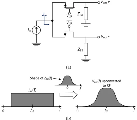
Considering the circuit of Figure 2.23a, from [22] is possible to conclude that the switches mix the baseband waveforms with the LO, translating its spectrum to RF, as shown in Figure 2.23b. Due to this effect, the input impedance aroundfLOis a
frequency-translated version ofZBB(f), i.e., ifZBB is a low-pass impedance (e.g. a capacitor), then
Zin(f)has a band-pass behavior. As will be analyzed in this work, this property can be
very helpful to filter undesired components of the RF signal. Another advantage of this kind of mixer is that a device in series with a current source does not change the current that passes through it, so its noise and non-linearity contributions are very reduced.
vLO
vLO
vout +
ZBB
vout
-ZBB
Iin
Zin
(a)
0 fLO 0 fLO
Iin (f)
0
Shape of ZBB(f)
Vout(f) upconverted
to RF
f f
f
(b)
As will be demonstrated later the passive mixers do not need to use a 50% LO duty-cycle, and the use of another duty-cycles (p. ex. 25%) can be very beneficial in terms of gain, noise figure, harmonic rejection, among others [23].
2.4.3 Active Mixers
Unlike passive mixers, this topologies provide conversion gain greater than one that helps to reduce the effect of noise generated by subsequent stages, as demonstrated in section 2.1.4.3. Due to this property, these mixers are very used in RF systems. The mixing operation is very similar to the passive mixers but instead of being used a MOS switch, a differential pair is used, as shown in Figure 2.24, that operates in the satura-tion region, and consequently provides current gain and high output impedance. In this structure, known assingle-balanced active mixer, the current source is controlled by the RF signal and the differential pair is controlled by the LO signal. It converts the vRF to a
current that flows to one branch of the differential pair (where it is amplified) according to the value ofvLO, and it is converted again to voltage by the resistorsRD, generating
the output differential voltagevIF. Since it is single-balanced, this mixer only operates
with a single-ended RF input.
v
IFv
LOv
RFR
DR
DV
DDFigure 2.24: Single-balanced active mixer (adopted from [3])
v
RFv
LOR
DR
DV
DDv
IFFigure 2.25: Double-balanced active mixer (adopted from [3])
2.4.4 Discussion
In this section two main mixer architectures were presented: passiveandactive. The pas-sive mixers do not offer conversion gain but are very low power, have low noise and high linearity. Also, a passive mixer can be current-driven instead of voltage-driven, which have some advantages like baseband impedance transformation and low noise and non-linearity contributions. The active mixers have as main advantage the conversion gain greater than one that helps to reduce the noise contribution of the subsequent stages of the receiver, but have more power consumption, noise (since they have DC current they produce flicker noise), occupy more area due its complexity and have lower linearity.
2.5
RF Filters
With the growth of wireless communications the demanding of high-performance RF (or microwave) filters is becoming huge due to the limitations of the frequency spectrum and the consequently increase of communication standards. The frequencies that are used to transmit the information are closer to each other, which means that there are more interferers near the band of interest that need to be filtered in order to prevent the leakage of out-of-band inter-modulation products and harmonics to the receiver [25]. Due to this proximity, the filters must have an high Q factor, to suppress the nearest interferers, and low losses in the interesting band, in order to not attenuate the desired signals.
A key filter in a RF receiver AFE is the SAW filter, shown in Figure 2.26, that attenu-ates the out-of-band blockers at the input of the receiver and consequently prevents the LNA saturation. The major problem of this filter is that it is very expensive and bulky, and have insertion loss since is usually based in resonators [7]. In a passive filter based in resonators the insertion loss is inversely proportional to its bandwidth and resonator Q factor, and is proportional to the number of resonators [25]. Also, high-Q resonators are physically large. Active filters can be used to avoid this problem, since they have gain that compensates for the losses related with the resonators, but they suffer from harmonic distortion, increased NF and non-linearities [26]. In order to save in area and cost, filters based on resonators can be implemented in CMOS technologies and integrated in the re-ceiver chip. However, unlike the off-chip filters, on-chip filters have low-Q factor, limited tuning range and the integrated coils take large chip area. There are some techniques to increase the Q factor but they degrade the filter noise and linearity [9].
SAW
LNA
Antenna
RX
Figure 2.26: Receiver AFE input
use of off-chip SAW filters.
Bandpass Filter Quality Factor
The quality factor (usually referred as Q factor) is a key parameter to measure the perfor-mance of a BPF. The expression of the Q factor is given by
Q= ω0
BW, (2.46)
where ω0 is the filter center frequency and BW is the filter bandwidth, which is given by BW = ω2−ω1. Frequenciesω1 andω2 are the frequencies at which the magnitude response of the filter drops 3 dB relatively to its maximum value (at ω0), as shown in Figure 2.27.
ω ω0
0 ω1 ω2
Vmax
Vmax -3 dB
Figure 2.27: BPF frequency response and Q factor
Thus, the Q factor is a parameter that measures the filter sharpness (or selectivity) and as higher the Q factor is, the better is the filter. This means that an high-Q BPF can block undesired signals that are closer to the band of interest, comparing with a low-Q BPF.
2.6
Analog-to-Digital Converters
Although the incoming signals of a RF receiver are in the analog domain, since the phys-ical world is analog, with the evolution of the technology those signals began to be pro-cessed in the digital domain because digital systems are more simple, cheap and flexi-ble. To make this possible is necessary to employ an ADC, as shown in Figure 2.28, that converts an analog signal to the digital domain. Due to the performance requirements needed to digitize a RF signal, the ADC can not be moved towards the antenna because a converter that fulfill these requirements is impractical in actual CMOS technology. This is why the AFE has a very important role in wireless communications, because it converts the RF signal to an analog signal that can be handled by the ADC.
Bout is the digital output word generated by the ADC with respect to the analog input
![Figure 2.25: Double-balanced active mixer (adopted from [3])](https://thumb-eu.123doks.com/thumbv2/123dok_br/16584484.738698/54.892.206.649.138.542/figure-double-balanced-active-mixer-adopted-from.webp)