The design of the gate bias circuit that controls the switching action of the power stage transistors is the major challenge in this technique, especially for the power stage with more than two stacked transistors. This thesis presents design and simulation results of the buck-type DC-DC converter based on 45nm CMOS technology. The switching operation of the output stage is controlled by control signals for PMOS and NMOS stacked transistors.
Introduction
Motivation
Advanced CMOS technology is one of the best candidates for implementing integrated PMUs due to its mature processing and lower cost through mass production. Another advantage of 45nm CMOS is the lower on-resistance due to the smaller channel length. Another method is to use cascode transistor structure as the solution to keep the power stage transistor supply voltage within the breakdown voltage limit.
Outline
Higher power efficiency is achieved by integrating PMU (Buck DC-DC Converters) on the same chip with digital logic circuits in an advanced System-on-Chip design and by eliminating additional IC package and PCB connections. Low breakdown voltage and high leakage current are the main drawbacks of CMOS technologies. The bias circuit ensures reliable operation of all transistors with respect to a maximum breakdown voltage of 1.8 V in 45 nm CMOS.
Background Theory
- Linear Voltage Regulator
- Switched Mode Converter
- Buck DC-DC converter
- Cascode power stage for input voltage up to 2VDD
- Cascode power stage for input voltage up to 3VDD
- Cascode power stage for input voltage up to 4VDD
- Design In Nano-Scale CMOS
- Reliability Issues
- Breakdown Mechanisim
- Cascode Circuit Architecture
- Literature Survey
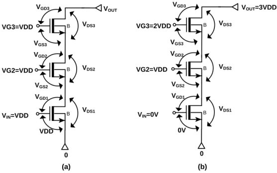
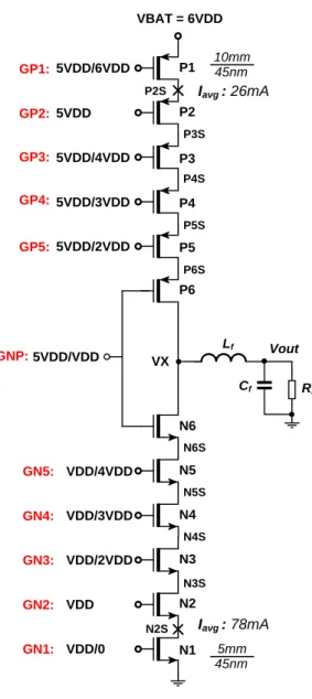
The inductor current ripple can be obtained according to the voltage of the inductor and the output voltage as shown in equation (2.3). In the circuit shown in Figure 2-5, the gate oxide voltage across each transistor of the stack is considered VDD. The power stage MOS transistors are built in single gate oxide form and biased with a voltage of Vcore = 1V.
![Figure 2-2: Ideal series-parallel step-down switched capacitor DC-DC converter [4].](https://thumb-eu.123doks.com/thumbv2/9pdfco/1890459.266625/11.892.330.641.614.754/figure-ideal-series-parallel-step-switched-capacitor-converter.webp)
Cascode Power Stage
Design Procedure
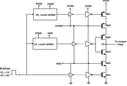
- Bias circuit for PMOS Power Transistors
- Bias circuit for NMOS Power Transistors
- Decoupling Capacitors
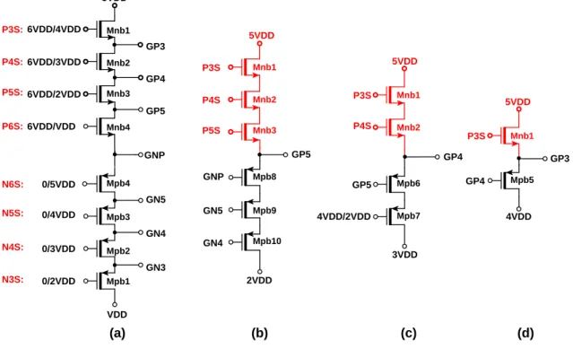
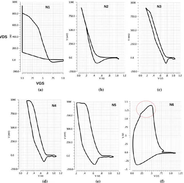
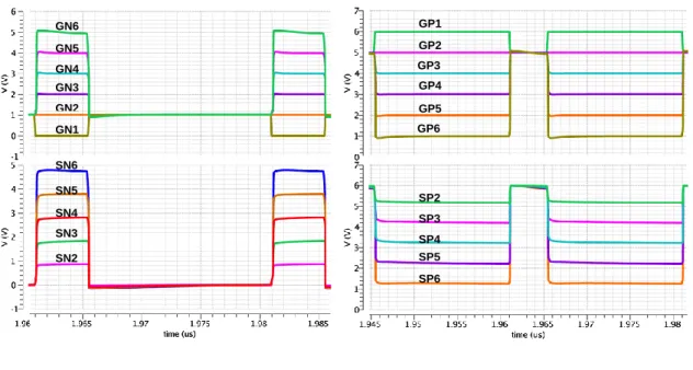
In the off state, for stacked PMOS transistors, P1 will first turn off, and then the bias state of the other transistors will depend on the dead time from high to low, according to the switching operation shown in Figure 3-12 and Figure 3-13. Therefore, the gate nodes will discharge to lower voltage levels even if N-Drive=0V as illustrated in Figure 3-13 for ZVS operation, however the discharge of PMOS gate voltages will be accelerated when the NMOS stage is on . The switching sequence for NMOS transistors starts with N1 and then the other transistors will turn on and hence the source nodes including N3S, N4S, N5S and N6S will discharge to 0V respectively and then VGN3, VGN4, VGN5 and VGNP as per Figure 3 - biased with reference voltage of VDD.
In this case from Figure 3-2 (b), GP5 will be discharged to 2VDD because VGN3, VGN4, VGN5 are biased with VDD and the circuit is supplied with reference voltage of 2VDD. Afterwards from Figure 3-2 (c), GP4 will be discharged to 3VDD as GP5 is already discharged to 2VDD. In the on state, discharge of the gate nodes starts when N1 turns on, after which the source of N2 will discharge, which will turn on the transistor N2, and then the source node N3S will begin to discharge.
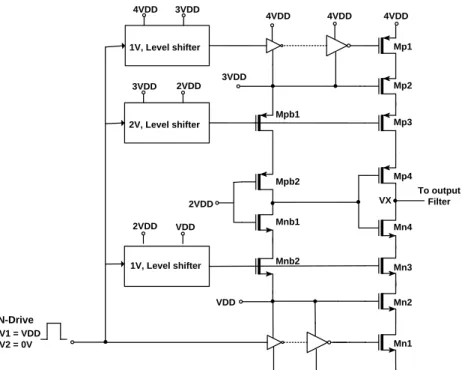
As shown in Figure 3-3(c), GN3 starts to discharge when N3S is discharged to 2VDD-Vth, then both GN3 and N3S are discharged simultaneously until N3S=0. The same operation is applied for GN4 and GN5, first N3S, N4S and N5S are discharged to 0V and then gate voltages are set to VDD. In the off state N1 will be turned off first, then N2S will be charged to VDD-Vth and N2 will be turned off, similarly N3S, N4S, N5S and N6S will start charging but continue charging depends on low to high dead time because, as shown in Figure 3-3 (a), the GN5 starts charging when the GNP voltage is higher than VDD+Vth.
Similarly, GN3 will be biased with 2VDD when Mnb5 is on as shown in Figure 3-3(c), and circuit (d) generates the required biases in Figure 3-3(b) when GP5 and GP4 are biased with 5VDD and the output voltage is 4VDD.
Power Stage Simulations
- Gate and source bias conditions
- Gate-Drain and Gate-Source voltages
- Hot Carrier Effect
- Non-ZVS Operation
All power stage transistors are biased with the required voltages for reliable power stage operation as shown in Figure 3-1. The state of gate oxide breakdown is studied by simulating VGD and VGS for power stage transistors as shown in Figure 3-7. As shown in Figure 3-12, charging of different PMOS source nodes does not occur at the same rate.
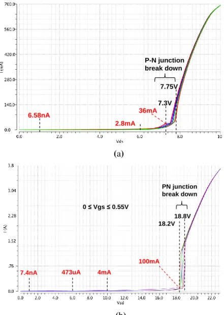
End points of the diagrams show VGS and VDS when a transistor is turned on and off, VGS value must be less than 1V to ensure reliable operation. These conditions do not satisfy the ZVS operation as depicted in Figure 3-12 (a) and (b) for VX node. In the low state, VX must be discharged to 0V before N1 is turned on, which is illustrated in Figure 3-13 (a). Increasing the high-to-low dead time, as shown in Figure 3-13 (a), can discharge VX node before N1 turns on, but diode conduction can occur when DTHL is increased to more than 200ps.
Simulation results for non-ZVS operation with L=68nH show that a small negative current from the inductor (-41mA) cannot charge the Vx node during the short dead time (100ps), so to avoid body diode conductance the dead time increases and decreases the inductor value at the same time is suggested. Negative current of -203mA can discharge Vx node with less dead time required for ZVS operation. Since a small inductor provides a higher resonant frequency, the output voltage ripple is reduced to 41 mV, as shown in Figure 3-14.
Therefore, there should be a compromise regarding ZVS operation and power loss due to high inductor current ripple.
Buck Converter Design and Simulations
- Design Specifications
- Circuit Block Diagram
- Optimization of Power Stage
- Level Shifter
- Global Bias Circuit
- Non-Overlapping Switching Circuit
- Schmitt Trigger
- Filter Components
- Parasitic Effects
- Simulation Test Bench
- Simulation Results
- Output Waveforms
- Switching Noise Effect
- Power Conversion Efficiency
The driveability of the circuit depends on the level shifter's requirements for rise and fall times. Power stages contribute to the power consumption of the main biasing circuit and the total power loss of the converter. Amplitude and offset of the input signal specify the duty cycle of the output signal.
Therefore, equations (2.3) and (2.4) are used to calculate the filter components and the values obtained are L=100nH and C=100nH. The buck converter test bench includes the DC-DC converter blocks and parasitic components in the PCB and IC package. Package parasitics, as depicted in Figure 4-14, consist of the wire frame and the bonding wire effects.
Due to parasitic inductance of the PCB traces, voltage ripple against the power supply increases. Noise from the input supply (VIN package) and VSS nodes generate the switching noise on the global bias circuit shown in Figure 4-17. The efficiency of the complete test bench is obtained by calculating the power loss of all parts of the simulation test bench.
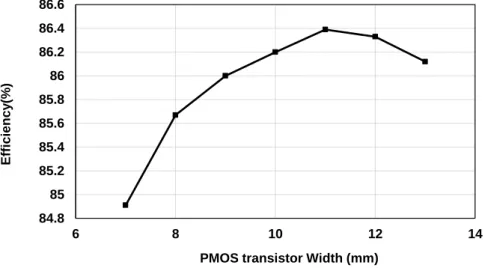
Optimizing the power stage has a significant effect on improving efficiency by selecting appropriate transistor sizes. High output current is required to charge and discharge the gate capacitance of the power stage transistor. Charging and discharging the decoupling capacitors during high and low states causes power loss.
Buck Converter with Variable Battery Supply
Proposed Circuit
The gate bias circuit in Figure 5-1 is designed to operate in different modes depending on the battery voltage values as shown in Table 5-1. In this case, when the output voltage VX=VBAT, transistors Nb1, Nb2 and Nb3 are on and Pb1, Pb2 and Pb3 are off. This ensures that for this battery voltage range, the gate-source and gate-drain voltages of all transistors remain within 1.5 V below the breakdown voltage.
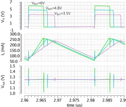
The slight deviation from 3 V is due to the fact that transistor Nb3 in Figure 5-1 operates in the subthreshold region. However, the other two nodes, GP3 and GN4/GP4, have a bias equal to VBAT-1.5V over the entire range of 3.5V Using the proposed gate bias circuit, for the entire battery voltage range of 3.5V Capacitance values are chosen to give the same RC delay time and therefore the same discharge rate at the gate nodes of all transistors in the power stage. The output voltage of the power stage VX, the inductor current IL and the output voltage of the converter Vout are plotted for three different values of VBAT=3.5V, 4.8V and 6V. The buck converter operates in continuous conduction mode with a maximum inductor current ripple of 200mA for VBAT=6V. The switching noise in IL and Vout can be improved by using a high-Q inductor with lower parasitic capacitance and higher resonant frequency in the output filter. For the discrete inductor Lf=100nH, we have used spice model of a TDK SMD inductor in our simulation [18]. A maximum power conversion efficiency of 81.3% is achieved for VBAT at 3.9V, and it remains above 72% for the entire battery voltage range from 3.5V to 6V. 34;High-voltage-tolerant linear regulator with fast digital control for biasing integrated DC-DC converters," Solid-State Circuits, IEEE Journal of , vol.42, no.1, pp.66,73, January 4] Wish, Mike, Steyaert, Michiel," Design and Implementation of Fully Integrated Inductive DC-DC Converters in Standard CMOS", Springer 2011, Chapter 2, Page 36. 8] Serneels, Bert, Steyaert, Michiel," Design of High Voltage xDSL Line Drivers in Standard CMOS”, Springer 2008. 12] Hyunseok Nam; Youngkook Ahn; Jeongjin Roh, "5-V Buck Converter Using 3.3-V Standard CMOS Process With Adaptive Power Transistor Driver Increasing Efficiency and Maximum Load Capacity," Power Electronics, IEEE Transactions on , vol.27, no.1, pp.463,471, Jan.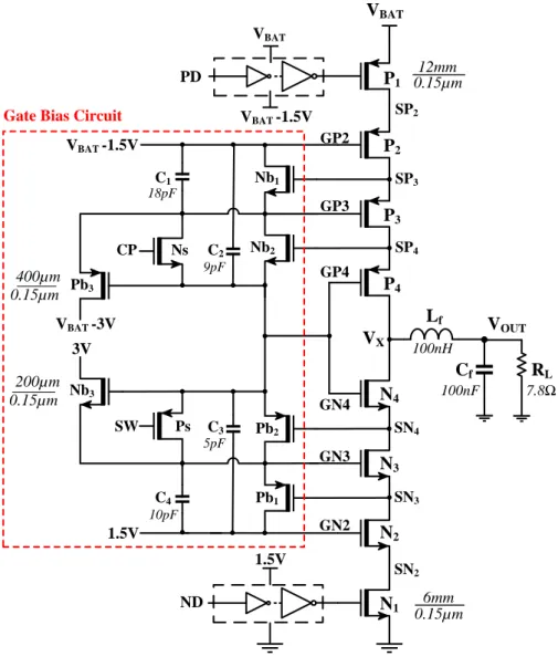
Simulation Results
Conclusions
![Figure 2-4: Steady state waveforms of the converter in continuous conduction mode (CCM) (a) Vx , (b) Vout and (c) Iout [7]](https://thumb-eu.123doks.com/thumbv2/9pdfco/1890459.266625/14.892.311.666.105.422/figure-steady-state-waveforms-converter-continuous-conduction-vout.webp)