Moreover, the power consumption of a device is one of the most important parameters, especially for wireless and mobile applications. The master's thesis, "Inkjet Printed Circuits on Fibrous Substrates for Environmentally-Friendly Radio-Frequency Electronics Applications", was carried out as partial fulfillment of the requirement for the master's degree in Radio Frequency Electronics major, in the Department of Electronics and Communication Engineering. at Tampere University of Technology.
Introduction
Electromagnetics Theory
- Electric Field
- Magnetic Field
- Maxwell’s Equations
- Wave Equations
- Plane Wave
- Energy and Power
- Transmission Line
- Scattering Parameters
- Microstrip Line
The complex power flow from the boundary of the volume V can be calculated as. The ratio of the incident voltage to incident current is Z0, while in the load this ratio should be.
![Figure 2.1. Different polarization types. (a) Linear, (b) elliptical, and (c) circular polari- polari-zation [11]](https://thumb-eu.123doks.com/thumbv2/9pdfco/1890707.266873/14.892.203.794.706.1083/figure-different-polarization-linear-elliptical-circular-polari-polari.webp)
Basic Theory of Antenna
How an Antenna Radiates
Antennas Parameters
- Radiation Pattern
- Half Power Beam Width (HPBW)
- Directivity and Gain
- Input Impedance and Return Loss
- Bandwidth
- Polarization and Axial Ratio
The angle between the points in the main lobe where the magnitude of the radiated power is half the pick value is called HPBW [13]. The ratio between the maximum power density (W/m2) and the average value (W/m2) is the directivity of an antenna. 3.3) where is the radiated power from the antenna and is the power loss due to the ohmic loss of the antenna [11].
Thus, the definition can be the ratio between the gain of an antenna and the gain of an isotropic antenna (which radiates equally in all directions) or the gain of a dipole antenna. In the first case, the gain unit is dBi, and in the second case, dBd. The real part represents the losses and radiation of the antenna, while the imaginary part shows the energy stored in the near field of the antenna [13].
3.6) Return loss or reflection loss represents the reflection of the signal when the transmission line is connected to a load or device. In this definition, the return loss of the antenna is higher than 10 dB in the entire frequency band [12].
![Figure 3.1. The representation of E-plane and H-plane of an aperture antenna [12].](https://thumb-eu.123doks.com/thumbv2/9pdfco/1890707.266873/19.892.276.739.173.520/figure-representation-e-plane-h-plane-aperture-antenna.webp)
Inkjet-Printing Technology
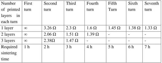
For both dielectric and conductive inks, curing or sintering after printing is essential. The temperature and time in the sintering process have a significant effect on the conductivity of the printed tracks. The metal components used in conductive inks are usually silver, gold or copper nanoparticles with 2 to 4 times higher resistivity than their pure counterparts.
Effect of sintering on conductive ink: (a) before sintering and (b) after sintering at 180 for 10 minutes. The printer used in this project is a Fujifilm Dimatix DMP-2831 material inkjet printer, shown in Figure 4.3, with a 210mm by 310mm plate area. Plate and cartridge temperature can be controlled with 1 precision in the range of 40 to 60 for plate and 28 to 35 for cartridge.
Each cartridge has 16 nuzzles spaced 254 µm in a single row, the volume of the droplets is 10 pL and the pulse voltage can be assigned between 18 V and 35 V. The resolution of the printed patterns can be specified from 100 dot - per-inch (dpi) up to 5080 dpi depends on the droplet size on the substrate. a) Dimatix DMP 2831 material inkjet printer.
Characterization of the substrate and conductor ink
Characterization of Cardboard
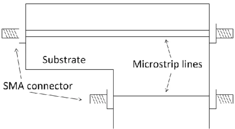
The effective dielectric constant of the substrate can be obtained by measuring the phase difference of the output signals in the lines. In a general loss transmission line, the magnitude of the output power Pout can be determined by knowing the magnitude of the input power Pin and the propagation loss α. In this case equation (5.6) can be rewritten as. 5.7 ) where llong is the length of the longer line, lshort is the length of the shorter line and the length difference between the two lines.
Since the conductor properties must be known for the characterization of the substrate, copper tape is used to implement the microstrip lines and ground planes. The conductivity, thickness and width of the copper microstrip lines implemented on cardboard are 5.8×10⁷ S/m, 50 µm and 2 mm, respectively. The thickness of the cardboard is 560 µm and it was kept in a regular oven with air circulation at 150 for 1 hour, since for inkjet printed circuit the same condition is used for sintering the silver ink.
For loss tangent using equation (5.7) the total propagation loss of the line is calculated, using equation (5.10) conductor loss is obtained. The measurement results for the loss tangent of cardboard using two transmission line method and dielectric probe.
Characterization of the Printed Silver Ink
They produced microstrip lines on cardboard using silver ink to find the conductivity of the printed silver traces. The value obtained for the conductivity of the printed silver traces is in this case 1×10⁷ S/m. The thickness of the conductor is an important parameter that affects the high frequency losses in the entire circuit.
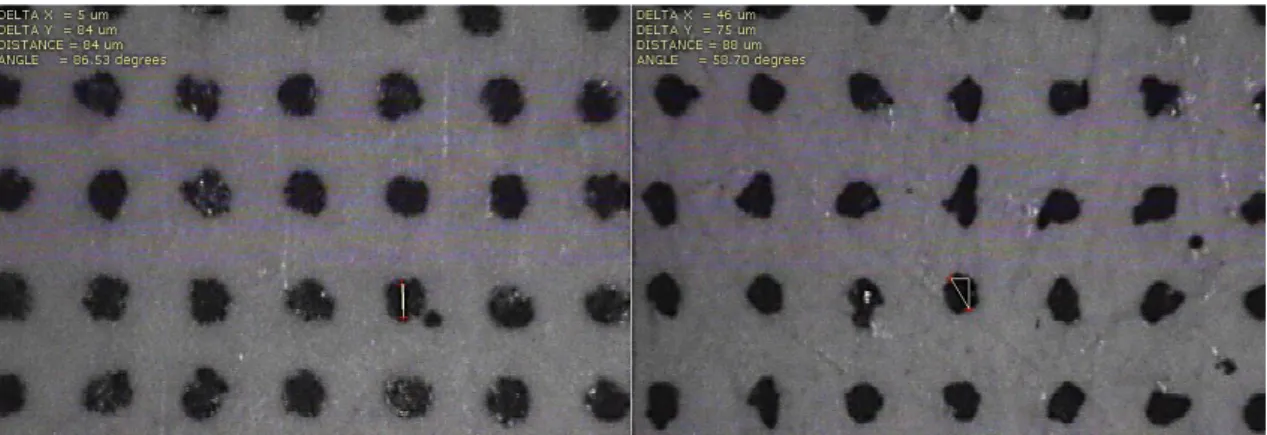
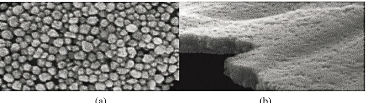
The examination of the thickness of the printed silver traces shows that the ink penetrates the substrate due to its fibrous nature. In addition, it is advantageous if this material increases the roughness of the surface, because high roughness values increase the high frequency losses. The cross-section of the printed silver traces on cardboard before and after treatment is illustrated in Figure 5.7.
The results for the roughness of the rough side of the cardboard before and after treatment and the smooth side of the cardboard are presented in Figure 5.8. a). To determine the conductivity of printed traces of silver after surface treatment, three microstrip lines with the above physical dimensions are implemented and the value obtained in this case is 2×10⁷ S/m.
Implementation of RF Circuits
- Band Stop Filter
- Patch Antenna
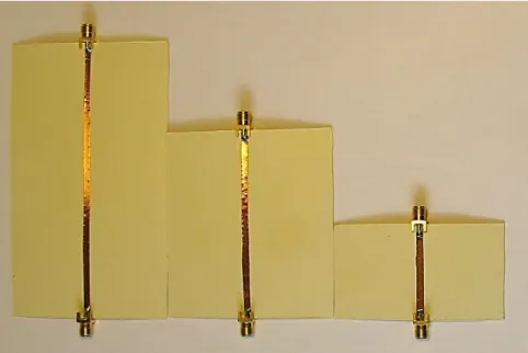
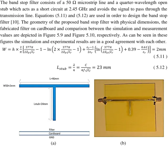
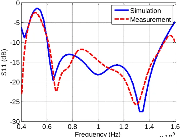
The geometry of the proposed bandstop filter with physical dimensions, the manufactured filter on cardboard and comparison between the simulation and measurement values are depicted in Figure 5.9 and Figure 5.10 respectively. As can be seen in these figures, the simulation and experimental results agree well with each other. a) The geometry of the proposed bandstop filter with physical dimensions. The simulation and measurement results for return loss, realized gain and radiation efficiency of the patch antenna are illustrated in Figure 5.12.
The simulation and measurement results of the inkjet printed patch antenna on cardboard for (a) the radiation efficiency, (b) maximum realized gain and (c) return loss. The comparison between the simulation and measurement results of the new simulation model is presented in Figure 5.15. The simulation and measurement of the patch antenna considering the low-misalignment for (a) the radiation efficiency and (b) maximum realized gain.
Simulation and experimental results for the normalized radiation patterns of the inkjet printed patch antenna using the obtained model are shown in Figure 5.16. Simulation and measurement results for the radiation patterns of the inkjet printed antenna.
Wide Band Antenna
Theory of Planar Wide Band Antenna
- Planar Multiresonator Broadband Microstrip Antennas
- Multilayer Braodband Microstrip Antennas
- Stacked Multiresonator Microstrip Antennas
- Broadband Planar Monopole Antennas
In addition, the overall size of the antenna is large and the radiation pattern changes with frequency, which is not suitable for the desired application [19]. The overall size of the antenna is not increased using this method, but the thickness is increased [19]. With this method, it is possible to achieve up to 70% bandwidth with a small variation of the radiation pattern with respect to frequency [21], [22].
But the implementation of the antenna on cardboard using this method is complicated, since it is difficult to stack different layers of cardboard and the appropriate facilities are needed [3]. A monopole antenna consists of the radiating branch and the ground plane, is one of the basic antennas' geometry. The first resonance of monopole antenna occurs when the length of the radiating branch is quarter wavelength [12].
The radiating branch is perpendicular to the ground plane which in the ideal case is the size of the ground plane to infinity. A planar monopole antenna is a monopole antenna in which both the radiating branch and ground planes are in parallel planes.
Design Procedure
Simulation results of input matching of the proposed rectangular monopole antenna for different values of W50. Input matching simulation results of the proposed rectangular planar monopole antenna for different values of p. For the next step, the feeding microstrip line is connected to the antenna using a tapered shape in order to improve the bandwidth and antenna matching [23], [24].
Having a tapered shape between the feed line and the radiating part of the antenna transfers some of the line impedance to the antenna impedance and reduces reflections and mismatch. As can be seen, the bandwidth of the antenna increases while the match at some frequencies is degraded. For the last step, in order to improve the bandwidth and match two slits are cut from the monopole pattern and one slit from the ground plane.
The geometry and simulation results for the final design of the antenna and its simulation result are illustrated in Figure 6.7 and Figure 6.8 respectively.
Simulation and Measurement Results
By comparing the simulation and measurement results of the maximum gain and total efficiency of the antenna, it can be concluded that the antenna works well. The other parameters that are beneficial to be investigated are the radiation patterns of the antenna. The simulation and measurement results of the E-level and H-level at different frequencies are presented in Figure 6.13.
The measurement at 600 MHz is done in EMC room and the rest in Satimo Starlab. It can be seen that in most of these frequencies the results are in an acceptable range. The E plane is like normal monopole radiation patterns at lower frequencies, while in higher frequencies the main beam is tilted towards the peak of the antenna and sidelobes appear in the lower parts as expected.
It can be seen that the maximum magnitude of the current appears around the two gaps in the monopole structure and the gap in the ground plane throughout the frequency interval of operation. In addition, the current distribution is relatively high in the outer part of the radiation flanks, which increases the radiation and bandwidth of the antenna.
Conclusion
34;Optimization of Inkjet Printing of Patch Antennas on Low Cost Fibrous Substrates" Hossein Saghlatoon, Lauri Sydänheimo, Leena Ukkonen, Manos M. 34;Optimized RF/Microwave Antennas and Circuits on Low Cost Fibrous Substrates Using Inkjet Printing Technology" Hossein Saghlatoon, Lauri Sydänheimo, Leena Ukkonen, Manos M. Tentzeris, 2014 IEEE International Symposium on Antennas and Propagation AP-S 2014, Memphis, USA, (Accepted for Oral Presentation).
![Figure 3.2. The illustration of a typical radiation pattern with its different sections [13]](https://thumb-eu.123doks.com/thumbv2/9pdfco/1890707.266873/19.892.254.719.756.1010/figure-illustration-typical-radiation-pattern-different-sections.webp)