ACADEMIC DISSERTATION Presented, with the permission of the Faculty of Engineering and Natural Sciences. All the publications included in this thesis are the result of the work done by many people.

Requirements for LIDAR applications
Other factors affecting spatial resolution include the frame rate of the LIDAR system and the repetition rate of the laser pulse. The main influence of the spectral width of the laser used in a LIDAR system results from the filters that can be used in combination with the detectors.
![Fig. 1.1 Artist’s depiction of a LIDAR working in challening weather conditions. [33]](https://thumb-eu.123doks.com/thumbv2/9pdfco/1890035.266201/29.748.163.607.169.332/fig-artist-depiction-lidar-working-challening-weather-conditions.webp)
Requirements for second harmonic generation
The wavelength acceptance bandwidth depends on the nonlinear material, fundamental wavelength, and crystal length. The requirement for wavelength stability comes from the acceptable wavelength band of the used SHG technique.
Overview of the publications and the state of the art
This enables confinement in one direction along the length of the crystal, while enabling higher input powers compared to 2D confining crystals. This makes coupling of light the easiest compared to 1D and 0D crystals, as there is no small waveguide to target with the input beam, but the beam diverges inside the crystal so tight focus along a long distance cannot be achieved.
![Fig. 1.5 State-of-the-art published and commercial results from tapered [69–72] and broad-area laser diodes [73–77] and the results discussed in this thesis as a comparison [PubI, PubII, PubIII].](https://thumb-eu.123doks.com/thumbv2/9pdfco/1890035.266201/38.748.155.566.119.456/published-commercial-results-tapered-results-discussed-comparison-pubiii.webp)
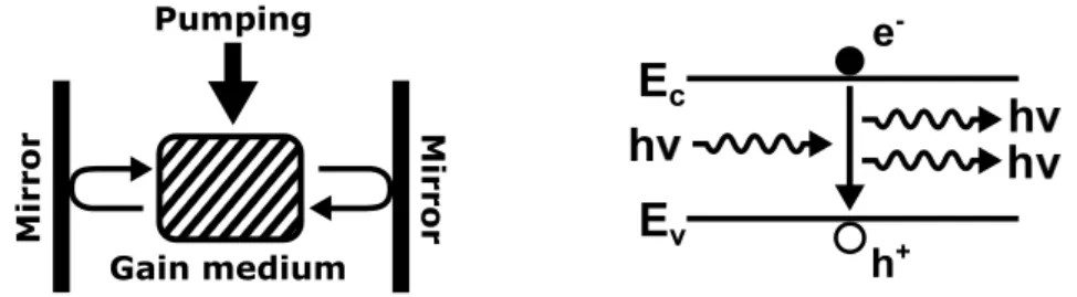
General laser operating principle
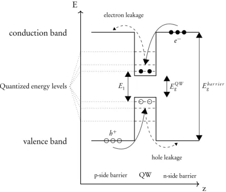
The QW is a thin layer with a thickness in the range of the de Broglie wavelength of the injected electrons and holes, so that the electron and hole energy states in the conduction and valence bands, respectively, become discrete. Around the QW there are cladding layers that provide carrier confinement, waveguide layers (also called optical confinement layers, OCL) provide optical guidance perpendicular to the growth direction of the semiconductor, which means that the refractive index of the layers is chosen such that the photons generated in the quantum well are guided parallel to the quantum well plane, and contact layer to improve current conduction and reduce the resistance between the contact metal and the semiconductor.
Cavity modes
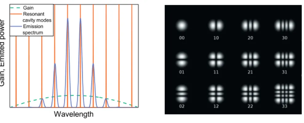
Conversely, if the optical round-trip length of the cavity is (m+1/2)λ, the interference is destructive and these wavelengths are attenuated. The combined effect of the gain bandwidth and supported cavity modes is the comb-like emission spectrum shown on the left side of the figure. The start, end, and envelope of the comb in wavelength space are determined by the gain bandwidth and peak-to-cavity spacing.
Often the cavity is so long that the neighboring peaks begin to overlap in spectral measurements and only the envelope of the peaks is seen unless extremely high resolution is used. In an FP laser cavity, all resonant cavity modes are almost equally supported by the cavity, since the reflectance of each mode is approximately equal at both mirrors, varied only by the dispersion of the effective refractive index of the mode at the facet of the cavity, the effect of which is usually negligible.
Wavelength locking with Distributed Bragg reflector
Cavity elements can also be inserted outside the gain chip forming a so-called external cavity laser. The DBR laser affects the intensity distribution of the resonant modes by making it dependent on the reflection wavelength of the mirror. In this way, if the wavelength range in the middle of the gain band can become highly reflective and provide strong feedback while the faces are almost transparent at the edges of the gain band, only the cavity modes in the center of the band can support lasing.
The strength of the grating and mode interaction can be characterized by a coupling constant (also called coupling coefficient)c: [86]. With a low total lattice reflection, the width of the reflection band can be calculated as [87].
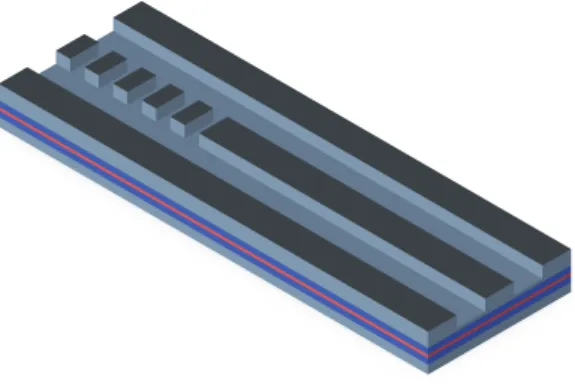
Surface grating DBR lasers
The grille profile, in particular the angle between the grille walls and the surface and the rounding of the edges at the bottom of the grille line, also influence the c. [92] An example of a V-shaped grid used in [PubII] is shown in Fig. The gain difference is a result of the shape of the gain bandwidth provided by the active region and the mirror loss difference is a result of the reflectivity of the grating and the longitudinal mode spacing of the cavity. The mirror loss is related to the threshold gain and the internal losses of the laser by [94].
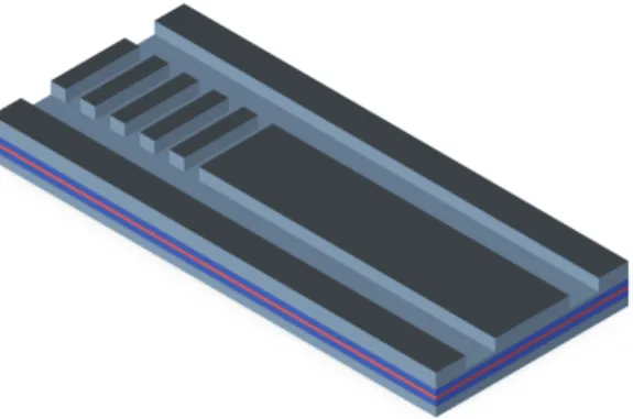
The front face reflection, if flat, has no effect on changing the mirror loss of adjacent cavity modes. The DBR grating period is 511 nm, grating length 2 mm, total cavity length 5 mm, and grating etch depth 50 nm above the waveguide.
Power and brightness scaling with tapered lasers
Separate injection currents can be applied to the RWG section and the taper section to have more control over the operation of the device. Only the optical field that strikes near the optical axis at the tapered facet contributes to feedback in the cavity, and the rest of the reflected light disappears axially in the component. At high optical field intensities spatial hole burning takes place which locally changes the refractive index of the material.
This variation in the refractive index causes self-focusing of the optical wave and leads to filamentation[101]. Filamentation reduces the beam quality and is thus detrimental to the properties of the laser from an application point of view.

Beam quality and its influence to applications
The amount of astigmatism can vary at different operating conditions of the laser, which complicates the design of optical systems that use a conical laser as a source. A tapered laser produces a perfectly Gaussian beam only if the mode exiting the RWG section resonates only in the fundamental transverse mode and it expands in the tapered section without perturbations to its wavefront caused by refractive index variations. Problems with lasers containing tapered sections include self-focusing and filamentation that degrade beam quality.
In LIDAR applications, beam quality is most critical for point scanning implementations[37] and if a semiconductor laser is used as the base laser for a fiber amplifier, although in this case a high beam quality alone is not sufficient[103]. This way the vertical beam quality is good (if the separate emitters are vertical single-mode) and the horizontal beam quality is not a big problem because it only needs limited collimation due to the shape of the scan line.
Power scaling with wavelength locked BA-DBR lasers
For all lasers discussed in this thesis, the vertical size of the optical mode inside the laser follows the waveguide from the structure of the semiconductor layer. As a result, the mode inside the laser is very narrow in the vertical direction, and thus the vertical (also known as fast axis) far field is wide. In the horizontal direction, the optical field width is a result of the geometry of the horizontal waveguide or the area where the current is injected if no waveguide is present.
The components reported in peer-reviewed publications represent the tip of the iceberg in terms of the number of devices manufactured, with a large number of better or worse intermediate components not reported. In addition, other aspects of the work are discussed to which the author has made an important contribution.
Standard characterization methods
Laser diode development is in many ways an iterative process, where initial components are usually designed based on simulations and past experience and then refined in successive development iterations until the desired level of performance is achieved. The ILV curve describes how the output power and operating voltage of the laser diode behave when the injection current is varied. The voltage behavior can be used to assess the quality of the semiconductor structure or the metal-semiconductor connection, while the output power is often the most interesting parameter of the laser, and e.g.
The available power sources are Keithley 2400 SMU, Arroyo 4320 LaserSource, Newport model 6000 laser diode controller, DEI PCX-7420 CW/Pulsed Laser Diode Driver, and Keithley 2520 Pulsed Laser Diode Test System. In LDC5000 this is measured using a photodiode attached to a sweep arm that rotates around the front hemisphere of the laser diode.
Special characterization methods for this thesis
- Higher pulse currents, shorter pulses, pulse measurements
- Characterization of multi-section diodes
- Robust tabletop laser mounting blocks
- Beam quality measurement
Another limitation of the LDC5000 system is the optical power measurement in pulsed mode. Then, using the same laser parameters, the shape of the optical pulse is measured using a fast photodiode (a Thorlabs DET08CL 5 GHz detector was used in this thesis) and an oscilloscope. On the front right side of the interposing PCB, the DC connector for the secondary laser contact is visible.
The beam quality measurement setup consisted of the following parts and is shown in Fig. Adjust the limits of the optical path so that the waist of the beam is approximately in the center of the sweep.

Other developed methods
Photolithography and nanoimprint lithography mask design 62
All lithography used in the fabrication of the devices described in this thesis involves optically active polymer spread on top of the wafer. Photolithography masks are glass plates coated with a thin metal layer that conforms to the shape of the target etch pattern: the metal blocks the interaction of UV light with the photosensitive polymer in the chosen positions. A workflow has been developed for this in which all mask layers of the individual component variants are first designed and then these variants are stacked to fill the target mask area.
Masks often have (partial) translational symmetry on some layers, and sometimes when machining a device, alignment marks from the wrong row or column can be mistakenly used, causing failure of the outermost components on the mask or even the entire wafer. It was also much faster compared to the ALD system, and because of the anisotrophy of the growth and the size of the process chamber, it was possible to coat arrays of rods with ease.

Wavelength locked 1180 nm laser diodes
For the measurements, they were operated in CW mode by injecting a constant current of 350 mA into the RWG section, and the injection current in the taper section was increased to 10 A. The beam quality factor of the 1180 nm taper DBR lasers was not determined. reported in the publications included in this thesis, but were included in the M.Sc. The primary cause of the high values lies in the layer structure of the material, which was not originally optimized for tapered laser diodes.
The material used had a relatively high QW confinement factorΓ=1.00%, resulting in self-focusing and filamentation of the beam in the tapered portion[101]. The QW confinement factor of the newer material is 0.5% and it has an asymmetric waveguide structure, which explains the improved beam quality.
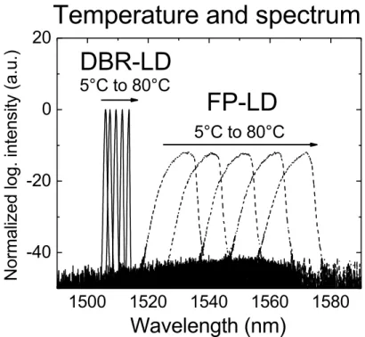
Wavelength locked 1500 nm laser diodes
At room temperature, the output power of the non-tapered and tapered DBR-LDs reached 655 mW and 4.04 W, respectively. Weiss, "The use of a novel yellow light laser (578 nm) for the treatment of class I red telangiectasia of the lower limbs", Dermatolic Surg., vol. The peak power of the DBR-LD and the FP-LD measured with 160 ns, 10 kHz pulses.
The spectra of the DBR-LDs were measured up to 40 A injection current with 160 ns pulses (Yokogawa AQ6375 optical spectrum analyzer) and up to 15 A with 1 µs pulses (Antritsu MS9710C optical spectrum analyzer). A typical full width at half maximum (FWHM) spectral width of the DBR-LDs was 0.30 nm. Left: Peak output power of the tapered DBR laser diode as a function of the current amplitude injected into the tapered section at 20 °C mounting temperature.
The effect of mounting temperature on output power was studied in both CW and pulsed modes of operation.
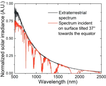
Extraterrestrial solar spectrum and spectrum incident on a ground-
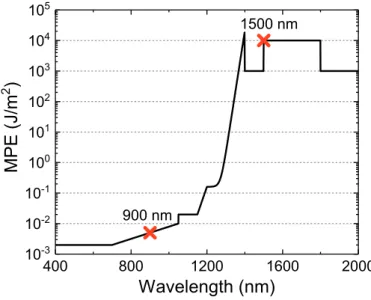
Maximum permissible exposure at the human cornea for various