G Transfer function controller on output Gco Transfer function control to output Gij Input of general transfer function matrix Gio Transfer function input to output Gio-f Ideal transfer function input to output Gs-in Input detection gain. Toi Output-to-input transfer function Toi-f Ideal output-input transfer function Ts Length of the switching period.
Photovoltaic Energy Systems
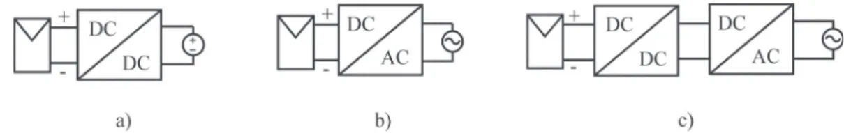
The basic elements of the PV power conditioning system are the dc-dc converter, single-stage dc-ac converter (inverter) and double-stage converter shown in Fig. power electronics in the system.
Issues Regarding Photovoltaic DC-DC Interfacing
The naming of the main classes is based on the type of input energy source, i.e. The validation methods of the MPP tracking converters also vary in the public literature.
Structure of the Thesis
The existence of RHP zero in a buck-derived PV converter has been recognized as early as the 1970s in [62] and later, e.g. The stability of a cascaded CF system can be evaluated using the inverse minor loop gain as discussed in [P2] and [P3] and also concluded in [87]-[89].
Objectives and the Main Scientific Contributions
It is shown how the intuitive method and explicit method based on duality principles have advantages over the third implicit method which is based on modification of existing VF converters. Limitations related to VF converters as well as the performance of explicitly and implicitly implemented CF converters are illustrated.
Introduction
Characterization of Arbitrary Switched-Mode Converter
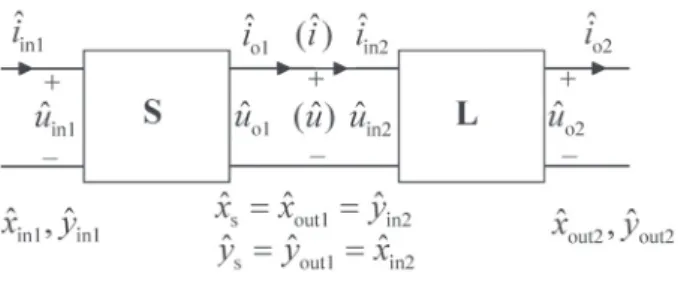
Converter under Feedback Control
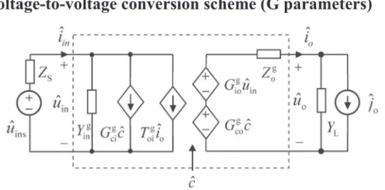
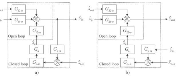
Feedback can only be taken from the output variables yˆin and yˆout, giving two different sets of closed-loop transfer functions. The input variable xˆr-out is the reference for the controlled variable, and the special transfer functions G11-f and G12-f are known as certain ideal transfer functions on the input side.
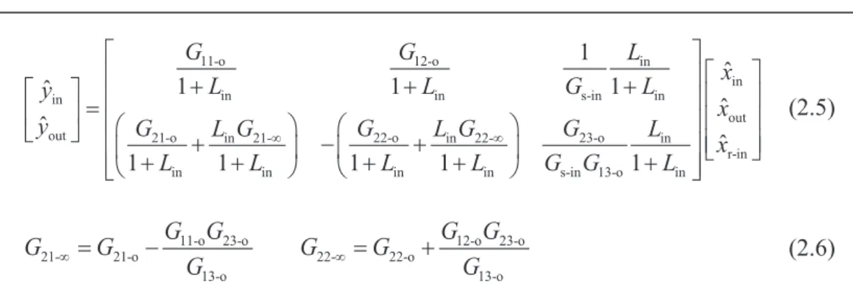
Effect of Non-Ideal Source and Load
Using the intermediate variables, it is possible to derive transfer functions affecting the load between the input and output variables as given in (2.13), where G22-xi denotes the ohmic characteristics of the output port when the input port is short-circuited (v in the case of the source input current) or in an open circuit (in the case of an input voltage source). The source and load transfer functions presented in (2.10) and (2.13) are naturally also valid in a closed loop.
Generalized Stability Assessment of the Interconnected Electrical Systems
According to the selected variables, the dynamics of the subsystems can be presented as given in (2.15) and (2.16). The stability of the interconnected system can be studied by constructing the mapping from the system input variables to the intermediate variables and to the output variables yielding (2.17) and (2.18). If the original subsystems S and L are assumed to be stable as independent systems, the stability of the interconnected system depends on term 1 / (1S L22 11).
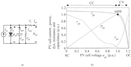
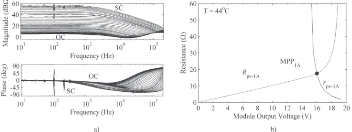
The DC resistance of the PV generator (source impedanceZs) is known to be positive resistance rpv corresponding to the static terminal resistance Rpv Upv/Ipv at MPP [P1],[P2],[23].
Conclusion
In the case of coupled VF systems, S L22 11 corresponds to the product Z Yo-S in-L, which is known as the minor-loop gain [85], where Zo-S is the output impedance of the source system and Yin-L the input impedance of the load system. In case of coupled CF system, S L22 11 corresponds to product Y Zo-S in-L, where Yo-S is the output admittance of the source circuit and Zin-L input impedance of the load circuit. The product Y Zo-S in-L is clearly the inverse of the VF system's minor-loop gain.
Therefore, instability in the Nyquist sense occurs at the MPP if the input impedance of the MPP tracking converter has the property of negative incremental resistance, i.e.
Introduction
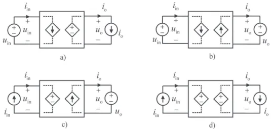
Intuitive Implementation
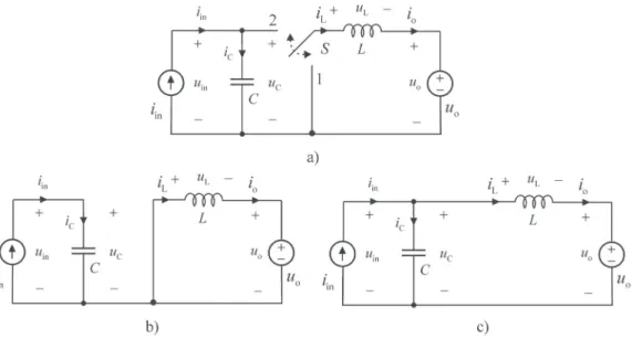
Step-Down Current Regulator
To decrease the load current, the current regulation must be adjusted to cut the input current. When the switch is switched to position 2 (Fig. 3.3c), the input current source is short-circuited and the charging current is maintained by the CL structure. Consequently, the output current can be chosen from (3.1) as a function of the input current and the duty ratio they provide.
If losses are neglected, the input power is equal to the output power (ie at in o o o.
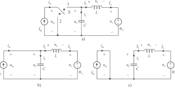
Step-Up Current Regulator
Since the duty ratio D is always equal to or less than unity, the step-down function of the current is obviously according to (3.2) and analogous to the conventional VF buck converter which steps down the voltage instead. Consequently, the output current can be solved from (3.4) as a function of the input current gain and the duty ratio. Since term (1/Dc) is always equal to or greater than one, the current-increasing nature of the converter is evident according to (3.5) and is analogous to the conventional VF boost converter, which instead increases the voltage.
Therefore, the converter is known in the literature as a dual boost or CF boost converter [78], [P7].
Explicit Duality Transformation
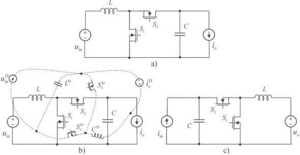
If the circuit is more complex and includes e.g. switching elements, the above-mentioned graphical method does not always lead directly to the desired result. The transformation can then be done in a convenient way by placing a dot inside each loop in the power stage and one dot outside the circuit and connecting the dots with a double branch lying between the corresponding dots. Following these procedures, the conventional synchronous HF boost converter shown in Fig. 3.6a, for example, can be transformed into its dual, CF boost converter.
It is known that the phase-shifting principle of the conventional VF power boost results in the following relationships between the input variables (input voltage and output current) and the output variables (output voltage and input current).
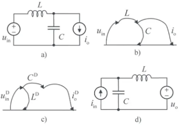
Implicit Duality Transformation
Finally, when the current source and capacitor are connected to the input terminal as shown in Fig. 3.8c, the power stage actually resembles the CF boost converter analyzed in the previous section rather than the conventional VF buck converter originally planned to be used. This can be avoided by modifying the circuit diagram so that the conduction time of the low-side transistor is determined by the duty ratio D. Due to the implicit nature of the duality transformation, it is generally not recognized that it has occurred.
The confusion is partly understandable because the basic physical relationships of currents and voltages in VF and CF boost converters are the same: the input voltage is higher than the output voltage and the output current higher than the input current in both cases.
Conclusion
This can be done by inverting the gate signals of transistors S1 and S2, giving The same effect can also be achieved by changing the polarity of the feedback and reference signals in the control system, or by using a falling PWM ramp signal instead of a normal ramp signal. The essence of power stage design, however, is to identify the correct input variables, which are constant in nature, and output variables, which can be controlled.
Open-loop analysis does not determine the inverter class per se, but the class can change if the controllable variable is not chosen correctly.
Introduction
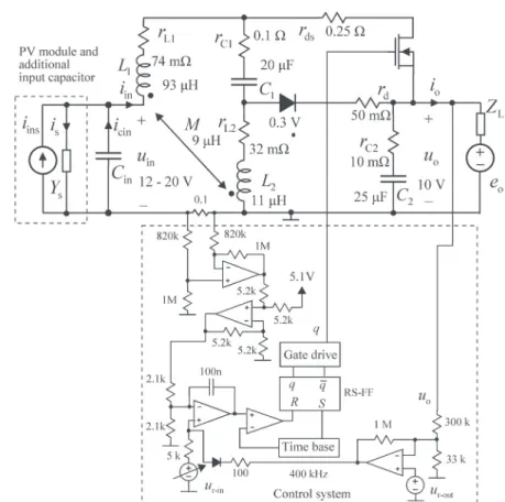
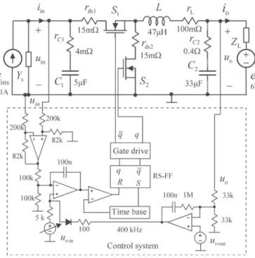
Test Environment and Properties of Photovoltaic Generator
The constant-voltage load at the output of the converter was provided by valve-regulated lead-acid storage batteries or Chroma 6312A electronic load. G.1b (see Appendix G); the input voltage of the coupling device varies and also changes the operating point of the PV module. This can cause confusion because the minus sign before the DC resistance is a property of the system in the stability evaluation, not the PV module.
However, the authentic source effects can be taken into account by measuring the frequency response of PV module impedance (or admittance), as illustrated in Fig.
Fourth-Order Buck Converters in PV applications
The studies show that the VF superbuck converter can only operate reliably in the CV region of the PV module due to the possibility of current loop controller saturation under input current control and impedance-based instability under output voltage control. Under the output voltage regulation, the input impedance of the CF superbuck is as given in (4.5) with the DC characteristics given in (4.6). The conclusion is that the power source characteristics of the PV module cannot be hidden by an input capacitor if the input current is controlled.
The saturation of the input voltage controller does not occur in a CF converter which enables the wide operating range.
Buck-Derived PV Converters
The theoretical input voltage range of the converter is from 6 V to 19 V due to the buck nature and level of output voltage (ie 6-V battery) and the PV module open-circuit voltage of 19 V. experiments confirm that the converter is indeed a CF boost -converter, not the VF buck, which was the basis of the converter's power stage. Since stable operation is only possible at a fairly high level of compensation, the behavior of the converter is basically similar to the input voltage-controlled CF boost converter, not the PCM-controlled buck converter.
Therefore, one should be aware of the true nature of the converter power stages and control methods used in the PV interface.
Conclusion
Experiments clearly show that using a conventional dollar converter can cause unwanted surprises when connecting PV. Feedback from the power stage inductor(s) currents is effectively a control method of HF converters that is not suitable for controlling CF converters, where the internal feedback must come from the power stage voltage(s) capacitor(s). This chapter contains summaries of papers [P1]-[P8], final conclusions and scientific contributions of the dissertation, and a discussion of future topics.
Summary of the Publications
It is pointed out that the CF converters can be implemented explicitly by duality transformation methods or by adding a capacitor at the input of the converter and controlling their input voltage. These papers examine the dynamic characteristics of the fourth-order buck converter or CF superbuck converter and its suitability for PV interfacing. The power stage of the converter is developed from the corresponding FF converter by applying explicit duality transformation methods.
The main results of the studies are that the converter works without limitations under input voltage control and MPP tracking, but the application of output control (to avoid battery overcharging) makes the system prone to instability.
Final Conclusions
It was also noted that the damping in loop gain can vary significantly due to the operating-point-dependent impedance of the PV generator. The PV interface is known to be challenging due to the highly variable terminal characteristics of the energy harvesting unit, i.e. the PV generator built from individual PV cells, which are basically current source in nature. This kind of transformation can produce unwanted surprises in the behavior of the converter if it is not recognized.
Due to the observed inconsistencies in the design of the photovoltaic converter, a generalized dynamic model of the switching converter was developed in the diploma thesis.
Future Topics
Moreno-Alfonso, "Power-Electronic Systems for Grid Integration of Renewables: An Investigation", IEEE Trans. Agarwal, "Maximum power point tracking scheme for PV systems operating under partially shaded conditions", IEEE Trans. Vitelli, “Low-frequency power oscillations and tracking of maximum power points in fuel cell-based grid-connected systems,” IEEE Trans.
Nagaraju, “Effect of Solar Array Capacitance on the Performance of a Switching Shunt Voltage Regulator,” IEEE Trans. Nehrir, “Direct Power Transfer for High Efficiency Photovoltaic Power Systems, Part I: Concepts and Hypotheses,” IEEE Trans. Ko, “Direct Power Transfer for High Efficiency Photovoltaic Energy Systems, II. part: An experimental evaluation,” IEEE Trans.