HAL Id: hal-00089174
https://hal.archives-ouvertes.fr/hal-00089174
Submitted on 11 Aug 2006
HAL is a multi-disciplinary open access archive for the deposit and dissemination of sci- entific research documents, whether they are pub- lished or not. The documents may come from teaching and research institutions in France or abroad, or from public or private research centers.
L’archive ouverte pluridisciplinaire HAL, est destinée au dépôt et à la diffusion de documents scientifiques de niveau recherche, publiés ou non, émanant des établissements d’enseignement et de recherche français ou étrangers, des laboratoires publics ou privés.
self-assembly to magnetic materials
Olivier Fruchart, Pierre-Olivier Jubert, Mustafa Eleoui, Fabien Cheynis, Bogdana Borca, Philippe David, Valérie Santonacci, Annick Liénard, Manabu
Hasegawa, Claire Meyer
To cite this version:
Olivier Fruchart, Pierre-Olivier Jubert, Mustafa Eleoui, Fabien Cheynis, Bogdana Borca, et al..
Growth modes of Fe(110) revisited: a contribution of self-assembly to magnetic materials. Journal of Physics: Condensed Matter, IOP Publishing, 2007, 19, pp.053001. �10.1088/0953-8984/19/5/053001�.
�hal-00089174�
ccsd-00089174, version 1 - 11 Aug 2006
Growth modes of Fe(110) revisited: a contribution of self-assembly to magnetic materials
O Fruchart, P O Jubert‡, M Eleoui, F Cheynis, B Borca, P David, V Santonacci, A Li´enard, M Hasegawa and C Meyer
Laboratoire Louis N´eel, CNRS, BP166, F-38042 Grenoble Cedex 9, France E-mail: Olivier.Fruchart@grenoble.cnrs.fr
Abstract. We have revisited the epitaxial growth modes of Fe on W(110) and Mo(110), and propose an overview or our contribution to the field. We show that the Stranski-Krastanov growth mode, recognized for a long time in these systems, is in fact characterized by a bimodal distribution of islands for growth temperature in the range∼250−700◦C. We observe firstly compact islands whose shape is determined by Wulff-Kaischev’s theorem, secondly thin and flat islands that display a preferred height,i.e. independant from nominal thickness and deposition procedure (1.4 nm for Mo, and 5.5 nm for W on the average). We used this effect to fabricate self-organized arrays of nanometers-thick stripes by step decoration. Self-assembled nano-ties are also obtained for nucleation of the flat islands on Mo at fairly high temperature, i.e.
∼800◦C. Finally, using interfacial layers and solid solutions we separate two effects on the preferred height, first that of the interfacial energy, second that of the continuously- varying lattice parameter of the growth surface.
PACS numbers: 68.55.-a, 81.16.Dn, 81.15.Fg, 75.75.+a
Submitted to: J. Phys.: Condens. Matter
‡ Present address: IBM Almaden Research Center, 650 Harry Road, San Jose, CA-95120, USA
Introduction
The first report of the epitaxial growth of the centered cubic element Fe along the (110) orientation was published more than twenty years ago[1]. Since that time a great number of publications have followed on the subject, with so far no sign of vanishing interest or slowing down of the discovery of new phenomena. The epitaxial growth under ultra-high vacuum (UHV) has mainly been performed on W and Mo, the two refractory metals than were shown to give rise to no or marginal interface reactivity at any temperature up that of thermal desorption[2], thus enabling one to fully explore the growth behavior.
In this article we will restrict ourselves to these two metals as a growth surface.
At first the interest arose for Fe(110)/W(110) because it appeared as a favorable system for an experimental realization of a model 2D magnetic system. The reasons were that 1. Fe and W are immiscible in the bulk 2. (110) is the most dense plane of centered cubic materials, thus ofa priori lowest surface energy and unfavorable against facet formation 3. W(110) surface energy (γW ∼ 4.0 J.m−2) is significantly larger than that of Fe (γFe ∼2.4 J.m−2), favoring wetting[3]. The immiscibility at the (110) interface was confirmed for Fe/W at all temperatures[2]. The single atomic layer (AL) was found to be pseudomorphic, and was thus a model system for calculations and analysis. The conditions are slightly less favorable for Mo, of surface energy γMo ∼ 3.4 J.m−2, and with alloys like Fe2Mo and Fe3Mo2 reported in the bulk and for which indeed marginal reactivity was reported at the Fe/Mo(110) interface above 525◦C[2]. This explains why the thorough investigation of epitaxial growth of Fe/Mo(110) started much later[4], finally revealing a behavior very similar to the case of Fe/W(110).
In short, Fe has a misfit close to 10 % with both Mo and W. For both Fe/Mo(110) and Fe/W(110) it was reported that at any temperature the growth begins by a pseudomorphic first AL, which above room temperature completes perfectly before the next layers start to grow. Then at elevated temperature further growth proceeds in the Stranski-Krastanov mode, whereas continuous although rough films are obtained at room temperature. More in detail, the following aspects have been reported: essential interfacial inertness[2, 5], atomic diffusion (W[6, 7] and Mo[8]), the growth and structure of the first AL [1, 9, 10, 11, 12, 13], the onset of dislocation formation and the structure of the interfacial dislocation network as a function of thickness (W[1, 11, 14, 15] and Mo[4, 16, 17]), the growth of continuous films (including characterization of stress and strain relaxation (W[12, 13, 15] and Mo[18, 19]), the kinetic roughness and a procedure for its smoothening[20, 21, 22], the formation of 1 AL and 2 AL stripes by step-decoration of vicinal surfaces and as a function of miscut azimuth (W[10, 23, 24, 25]), the onset of SK growth and nanostructures obtained by annealing or directly by high temperature growth (W[26, 27, 28, 29, 30, 31, 32] and Mo[4, 16]).
Some years ago we have considered Fe(110) magnetic systems in the context of the rising interest in self-assembly, i.e. the process by which nanostructures (wires, dots etc) can be spontaneously fabricated by deposition on surfaces. In the following we will use the term self-assembly (SA) when the nanostructures display no order or only
short-range order, and self-organization (SO) when the nanostructures display at least a medium range order[33]. In search of optimized growth procedures for the fabrication of SA or SO Fe(110) nanostructures we have undertaken a systematic investigation of growth processes in terms of substrate material, amount of Fe deposited, growth temperature and possible annealing. In this course we have gathered significant new data about the system, and uncovered new growth phenomena. Notice that our evaporation technique is pulsed laser deposition performed under strict UHV conditions. This technique yields results very similar to those obtained by molecular beam epitaxy[34, 8].
We indeed found noquantitative discrepancy with previously published data.
It is the purpose of this article to summarize our contribution to growth processes of Fe on W(110) and Mo(110) surfaces. We have already published several articles fully or partly related to the epitaxial growth of Fe(110). These concerned the principle of growth of high-quality buffer layers on Sapphire[21], the sub-monolayer range for Fe/Mo(110)[8], the occurrence of self-assembled Fe/Mo(110) compact islands and the deduction of the effective interfacial energy for this system[35, 36], the fabrication of nanometers-thick stripes by step decoration for both Mo(110) and W(110) surfaces[37, 38, 39]. The present article aims at giving an overview of our results, therefore some overlap with the above-cited articles is inevitable. Nevertheless we report here more details and new results. Besides, we report preliminary results using a more systematic approach. The first improvement consists in tuning continuously the in- plane lattice parameter from that of W to that of Mo, using solid solutions. The second improvement consists in controling independently from the previous point the chemical nature of the interface, either W or Mo, making use of ultrathin pseudomorphic interfacial layers. Applied to the subsequent fabrication of both islands or wires, this approach should in the future cast light on the relevant parameters involved in the process of self-assembly of Fe(110). Incidentally, this latest investigation has allowed us to further increase the versatility of Fe(110) nanostructures that can be grown.
1. Experimental procedures
The experimental growth setup has been significantly modified since its lastest description[35, 8] so that we describe it here in detail. It consists of three interconnected UHV chambers, each equipped with an ion pump with a Ti sublimator. The first chamber is used for samples and targets storage, and samples preparation and analysis.
It is equipped with a scanning Auger electron spectroscopy with MACII analyzer, scanning Argon ion etching (Thermo VG EX05), substrates outgassing (base pressure 2−3×10⁻¹⁰Torr). A turbo pump is directly fitted to this chamber for use during ion etching. The second chamber is equipped with a room-temperature Omicron STM-1 Scanning Tunneling Microscope with a maximum field of view of 800 nm (base pressure 5×10⁻¹¹Torr). The growth proceeds in the third chamber (base pressure 5 × 10⁻¹¹Torr). The evaporation method is pulsed-laser deposition (PLD) using a Quantel Nd-YAG frequency-doubled (λ = 532 nm) laser with pulse width around 10 ns,
a shooting frequency of 10 Hz and a maximum energy per shot of 150 mJ. The energy is adjusted by tuning the delay between the oscillator and the amplification stage of the laser while the pumping stays constant. The growth chamber is equipped with a 10 kV RHEED setup with a 10-bit CCD camera synchronized with laser shots, so that RHEED patterns and oscillations can be monitored during deposition. The laser beam enters the chamber through a window and impinges on the target at an angle 27◦ away from the normal to the surface. The main parameter for evaporation is the fluence F, i.e. the energy per shot and per unit area of the target[40, 41, 34]. F can be adjusted with both the laser power and a focusing lens located outside the chamber on the beam path. The focal length of the lens is 500 mm. The focus is located ahead of the target, at a distance 120−180 mm depending on the element to evaporate. The resulting working value lies in the range 0.1 −1 J/cm2, yielding a typical deposition rate of 0.5 ˚A/mn. The laser is rastered on the target with the help of anex situ mirror mounted on an electro-acoustic device. The substrate-to-target distance is 140 mm. A Cu foil placed before the sample can be moved continuously during deposition to mask part of the sample and thus fabricate wedge-shaped films, i.e. films whose thickness is varied from one place to another on a sample. In the case of simple wedges the direction of the movement of the mask is always progressively masking the sample. By rotating the sample around its axis by 180◦ a wedge with an opposite slope can be fabricated.
To switch over to another target the beam can be stopped with an ex situ mechanical shutter, another target is moved in front of the beam, and the focusing of the beam on the target is adjusted to a value suitable for each material. All these movements are motorized and controlled through a computer that allows one to launch macros, like the numerous opposite wedges necessary for the fabrication of solid solution buffer layers with continuously varying in-plane lattice parameter, as reported in the next section. The location on the wedge of the focused electron beam used for AES can be precisely and reproducibly controlled owing to a translation stage. The convolution of the translation uncertainty and the size of the spot on the sample is estimated to yield an uncertainty of 100µm. For quantitative AES the measurements are normalized to the beam intensity, which is measured regularly during each series of measurements on a reference part of the sample consisting of either a thick deposit or a bare buffer layer of a pure element.
All our film are deposited on commercial Sapphire Al203wafers. Wafers from several suppliers have been used (Union Carbide, Bicron, Crystal GmbH), without noticing significant differences on the crystal quality of the films grown on top. The miscut was found to vary from wafer to wafer, however is unchanged over the two-inch area. Typical values lie below 0.1◦. The sample holder consists of a modified one inch Riber Molybloc with a slot to insert an Omicron STM holder. One of the clamps holding the substrate is rotatedin situwith the Omicron wobblestick to scratch the surface of the sample and set an electrical contact for STM measurements. Openings have been made in both the molybloc and the STM sample holder, so that the rear of the substrate is in direct view of a Joule-heating filament. With this setup the sample size is 6.5×8.5 mm, sitting on a
500µm-wide ledge. To sit on this thin ledge the two-inch Sapphire wafers are precisely laser-cut in a dedicated ex situ chamber. To this purpose the Nd-YAG laser is focused on the backside of the wafer, with a spherical lens f = 200 mm. A set of two cylindrical lenses with identical flat axes, one convergent and one divergent however with shifted focal planes, is inserted before the focussing spherical lens. This provides us with a beam with a very elongated elliptical shape, in turned transformed with a diaphragm into a very narrow and nearly rectangular shape on the wafer, whose feature is a nearly constant energy per unitlength. With this design the wafer is cut much more efficiently than with a simple spherical focusing, because laser ablation suffers from a saturating effect above the evaporation threshold[40]. The linear cutting speed is then of the order of one millimeter per second. The wafers are then cleaned in an ultrasonic bath in 10-20 % diluted RBS25 (Chemical Products, Belgium), then rinsed with deionized water, to remove the Al deposited at the back during the laser cutting. The rear of the wafer is sputter-coated by sputtering prior to deposition with a 100 nm-thick layer of a refractory metal, usually W. The purpose of this layer is to absorb most of the heating radiation emitted by the filament on the deposition stage. Without this layer a significant amount of radiation is absorbed directly by the epitaxial film, resulting in higher and uncontrollable temperatures. Substrate temperatures up to 950◦C can be achieved with this setup, calibrated by an optical pyrometer and controlled routinely by a thermocouple in direct contact with the rear of the molybloc. Owing to this indirect measurement of temperature, error bars on temperature reading might be significant, especially in the range 25−250◦C because of thermal inertia. The sample can also be substituted with a quartz microbalance. Finally all deposits are capped before taking them back to air. The capping, deposited at room temperature (RT), may consist of 5 nm of Mo or W, or of a few atomic layers of either covered by a 2 nm of Al, Mg or Au.
The latter two are slightly annealed above room temperature to smoothen the surface.
All these capping procedures have been checked to result in a smooth layer displaying single atomic steps, and are an efficient barrier against oxidation of Fe.
Atomic force microscope images were performed on a Park Scientific Instrument Autoprobe CP in contact or non-contact mode. The Si tips are pyramidal (Mikromasch CSC21B, force constant 2 N/m). X-ray diffraction (XRD) was performed using several setups equipped with a monochromator. We worked essentially in a θ−2θ geometry, probing either diffusion vectors out of the plane, or in-plane with a grazing incidence.
In the following misfits are expressed with respect to the growing film, e.g. ǫ = (aMo−aFe)/aFe. Finally, for element A grown on B we use the notation A/B.
2. Growth of buffer and interface layers
We do not use metal single-crystals as a substrate, but instead we grow bcc(110) buffer layers on Sapphire Al203(1120). On the one hand this is more time-demanding than using metal single crystals as a new buffer layer has to be prepared for each new sample.
On the other hand it allows one to keep all samples and take them ex situ for further
1 mm
(a) (b) (c)
bcc[001]
Twin bcc[001]
Twin bcc[110]
bcc[110]
Sapphire[1-100]
Sapphire[0001]
//bcc[-1-1
1]
~35.26°
[001] 50nm [1-10]
[001]
[1-10]
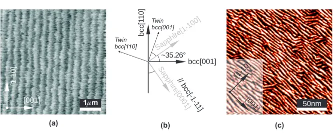
Figure 1. (a) 5×5µm AFM image of a typical Al203(1120) surface displaying an array of monoatomic steps after annealing at 800◦C for one hour under UHV. The vertical scale is 4 ˚A (b) epitaxial relationships between Sapphire and body centered cubic elements (bcc), revealed by XRD and RHEED. The majority relationship[43] is marked with dark lines and upright letters, while the minority twin is marked with thin lines and italicized letters (c) The size of the crystallites of the minority twin are revealed in real space by STM by the areas with a 70◦-rotated grooved pattern formed upon deposition at moderate temperature, see text.
characterization after growth. Most importantly, this allowed us to vary the composition and thus tune the in-plane lattice parameter, as will be shown in the following. We reported in the past the growth of high-quality single-crystalline Mo(110)[21] and Nb(110) buffer layers[42]. After recalling the growth procedure of such layers and give further characterization with respect to Ref.[21], we present three improvements that have been of use for the growth studies of Fe(110) reported here, namely the successful suppression of twinning for W(110), the fabrication of solid solutions with tunable in- plane lattice parameter, and the deposition of atomically-flat pseudomorphic ultrathin layers over these buffer layers.
2.1. Recall of the general procedure
The Sapphire wafers, prepared as reported above, are mounted on sample holders and outgassed under UHV at 800◦C for one hour and let cool down for one hour. At this stage the crystal surface consists of atomically-flat terraces separated by single atomic steps, whose separation and orientation are related to the residual miscut (Figure 1a).
The miscut was found to vary from wafer to wafer, however is unchanged over the two-inch area. A typical value for the terrace width is 200 nm (see FIG.1a,2f).
Buffer layers consist of bcc materials deposited on Sapphire. The growth process described in the following applies equally well for Mo, Nb and W, at least. The epitaxial relationship with Sapphire agrees with that reported already long ago[43] (Figure 1b).
These bcc materials are first deposited at moderate temperature. In the past we were starting the growth at room temperature (RT) and the heater was switched on around
(a)
(d)
(b)
(e) (110)
[-110]
[001]
(110)
[001]
[1-10]
(110)
[001]
[1-10]
(110)
[-110]
[001]
(f)
150nm [001]
[1-10]
(c)
50nm [001]
[1-10]
Figure 2. Characterization of Mo(110)/Al203(1120) films (a-c) after deposition at room temperature and (d-f) after deposition at room temperature followed by annealing at 800◦C. (a-b;d-e) RHEED patterns along two azimuths (color scale on the left). The sample lies vertical at the left of the screen. (c,f) STM images.
0.5−1 nm to reach 150−200◦C by 1.5 nm. We nowadays perform the entire growth at RT, with no detectable difference in the quality of the final annealed films, see next paragraph. Concerning the films before annealing, RHEED and STM show that after growth at moderate temperature their surface is rough (Figure 2a-c), displaying grooves oriented along [001], a common feature for bcc(110) epitaxy[20, 21, 22]. The microscopic origin of this anisotropy of roughness has been discussed in Ref.[20] and simulated in [22], on the basis of anisotropic diffusion at the nucleation stage, followed by a kinetic effect related to the Schwoebel barrier. In the former article the angle of the facets was investigated for Fe(110) for a few thicknesses up to Θ = 9 AL, at 200 K. It was found that this angle increases during deposition to reach a value close to 18◦. The authors could nicely reproduce their data with a model of layer-restricted-diffusion (LRD) growth. Our data partly confirm these conclusions. The arrow-like pattern of Figure 2a is blurred at the beginning of growth and sharpens upon deposition. However, whereas a LRD model predicts a steady increase of the mean angle upon growth, we evidence that the angle of the facets becomes stationary after some nanometers are deposited. RHEED and STM show in quantitative agreement that the stationary angle is close to ±19◦, coherent with facets of type {210} (see Appendix II). These values are consistent with the thickest deposits of Albrecht et al. dealing with Fe[20], although these authors did
not realize that a stationary value had been reached. The breakdown of the continuous LRD model may be due to a modification of the Schwoebel barrier, and/or to the modification of diffusion rates on the micro-terraces of the facets of type {210}, due to finite size and/or the discreteness of the terrace. Indeed the width of such a terrace is
7 2abcc
√2/2≃7−8 ˚A, and only three atomic rows sit on each terrace. In fact in Ref.[22]
it was already suggested that some type of facet should be stabilized, using geometrical arguments for impinging and diffusing atoms. However it was claimed that the {310} facets should be stabilized, contrary to our findings. The stability of the {210} facets has a positive effect on the array of grooves, whose distribution of local orientation and period decrease upon further deposition after the nominal facet angle has been reached on the average,i.e. after 1−2 nm. The array progressively thus becomes self-organized, see Figure 3.
The facetted grooves form upon deposition at temperatures below 225◦C[21] for Mo and 325◦C for W. We have recently evidenced with RHEED that the roughness becomes isotropic below approx. 100◦C for W. A similar lower bound is likely to exist for Mo and Fe, however shifted below RT in relation with the hierarchy of bonding strengths. In Ref.[20] facets were still observed for Fe at 150 K. As our setup cannot operate below RT we could not confirm this hypothesis. Nevertheless, the existence of a range of temperatures for the kinetic formation of grooves, and its quantitative determination for W, should be a valuable input for simulations, to determine the microscopic mechanism responsible for this growth phenomenon. These grooves may for instance be a valuable template for the self-organization of wires, like those obtained upon grazing-incidence ion etching[44, 45, 46]. With this in mind, let us add that STM investigations revealed that the order seems to be at its best somewhere in the intermediate range of temperatures, in terms both of alignement of the wires along [001], and of regular period along [1−10]. The quality of the order is then reflected by the occurrence of a superstructure on the RHEED patterns (Figure 3). The period deduced from RHEED is in accordance with the period observed by STM, i.e. around 5 nm for Mo or W deposited at 100◦C (Figure 3). The average depth of the grooves is 1 nm in this case. In Ref.[20] it was postulated that the period is selected during the nucleation stage in the sub-atomic layer range of deposition, and accordingly was found to increase when the temperature of deposition was increased. Although we have not investigated this feature extensively, we have noticed that both nucleation and growth temperatures play a role. Notice finally that all crossover temperatures between different growth modes may depend on the deposition temperature, and concerning PLD depend also on the laser ablation parameters. For instance, rather smooth films can be achieved at a temperature lower than the cross-over one for a higher laser fluence, which is explained by the higher mobility of adspecies when they impinge on the surface[8]. For an overview of differences between Molecular Beam Epitaxy (MBE) and PLD see Ref.[34].
As already reported[21], there exists a dual epitaxial relationship of refractory metals with Al203(1120), both sharing bcc[111] k Al203[0001]. The dominant relationship is bcc[001]∼kAl203[1102][43], associated with intense streaks on RHEED,
(a) (b) (c) (110)
[-110]
[001]
1.0 0.5
0.00 5 10 15 20
Distance (nm)
Height(nm)
25nm [001]
[1-10]
Figure 3. RHEED patterns on a grooved surface arising upon deposition of W(110) at 100◦C, along the (a) [001] azimuth (b) same as a, misoriented by◦1 away from [001]
so as to enhance the satellite structure of the [1−10] arrow-like streak (bottom). (c) STM image of the W(110) surface with a cross-section (arrow on the image).
whereas weaker streaks on the RHEED pattern can be attributed to a 70◦ in-plane rotated relationship, in other words mirrored with Sapphire (1100) plane. This was confirmed by grazing incidence XRD. The dual relationship is explained by the initial completion of the dense atomic rows along bcc < 111 > directions in the nucleation stage, followed by the completion of<100>directions of atoms at≈ ±35.26◦ on either side. The crystallites of the minority twin crystallites are easily revealed upon growth at moderate temperature from the local direction of the grooved pattern (Figure 1c).
For Mo the minority crystallites cover an area not exceeding 10 % of the surface, with a typical lateral size of 15 nm.
These layers are then annealed at 800◦C for 30 min to flatten the surface and improve the crystalline quality. RHEED patterns then display a sharp 1×1 pattern, and reveal that the minority twin has vanished in the case of Mo, however not in the case of W (upon a similar annealing the minority twin vanishes in the case of Nb and V layers, however not in the case of Ta. These three buffer layers have not be used for the overgrowth of Fe reported here). In the case of Mo the disappearance of twins can also be checked by redeposition of a bcc material at moderate temperature, in which case the array of grooves, locally aligned along [001], consists of one single domain. It is this procedure that has been used for Figure 2a-c. In Ref.[47] it was reported that Mo films deposited at 800◦C do not show this problem of twinning, however displayed a weak misorientation of crystallites in the as-deposited state, resulting in micro grain boundaries. It was shown using Low-Energy Electron Microscopy that these grain boundaries could be largely eliminated by annealing at 1425◦C as they then become
34
2q
36 38 40 42 44
102 103 104 105
Counts
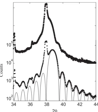
Figure 4. XRD in theθ−2θgeometry of a Nb film grown at 200◦C (top) and annealed at 800◦C (down). The dots stand for experimental points, while a qualitative fit of the Kissing fringes a shown in continuous line for the latter.
very mobile. In our case we never came upon any evidence of the existence of such micro-grain boundaries, in particular with STM. These annealed buffer layers consist of atomically-flat terraces separated by mono-atomic surface steps (Figure 2f). Large scale ex situAFM images show that these steps form a long-range ordered array on the sample, whose orientation and period are linked with the residual miscut of the wafer after polishing. Over a large number of wafers from various manufacturers the terrace size was found to vary from 100 nm to 400 nm, thus implying an average miscut angle around 0.05◦. Notice that the miscut was always found to be uniform over the entire two-inch wafer. Thus, as this wafer is cut into tens of sub-centimeter-size sub-wafers, once the miscut angle and azimuth are known from microscopy, spare sub-wafers are stored that can be used whenever a desired miscut is required.
The annealed buffer layers were characterized ex situ with X-rays. The measurements with the highest resolution were performed in the θ−2θ geometry to measure the out-of-the-plane q vector. No detectable deviation from the bulk lattice parameter was evidenced, within the accuracy of better than 0.1%. Kissing fringes with many orders are observed only after annealing, resulting from the finite thickness of the layer, confirming the flatness of both interfaces (Figure 4). For all films the crystalline coherence length equals the film thickness minus a few atomic planes that contribute to an amorphous oxyde layer at the free surface. In grazing incidence the epitaxial relationship was confirmed and the bulk lattice parameter was retrieved, within the experimental accuracy of 0.5%.
The deposition and annealing parameters are not critical to get these buffer layers
(a) (b) (c) [001]
[1-10]
2µm 1µm
5µm
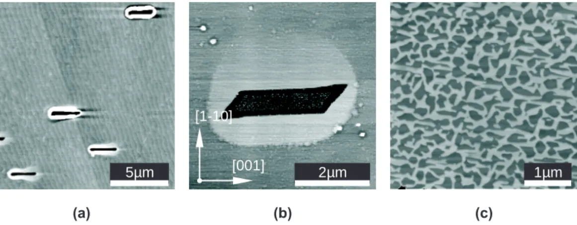
Figure 5. Unwetting of Mo(8 nm)/Al203(1120). (a) After annealing at 900±50◦C.
The array of monoatomic steps of Mo can be seen at the background. (b) same conditions, with now the atomic steps running along [001]. The steps are not clearly seen because the scan was performed along the same direction. On both pictures the hole created by unwetting is decorated by a brim of Mo, with a flat surface, such that it appears as wedged over the slightly vicinal continuous Mo buffer layer. The small irregular patterns, looking like islands, are Al islands arising from a protective layer deposited under non-optimized conditions. (c) A Mo film of nominal thickness Θ = 2.2 nm, which upon annealing at 900±50◦C unwets Saphir while forming nanostructures of height∼5.5 nm.
of high cristalline and topographic quality. However a minimum nominal thickness Θ = 8 nm is required to avoid the unwetting of the substrate during annealing at 800±50◦C. The Mo layers start to unwet sapphire for annealing temperatures above 900±50◦C or Θ < 8 nm (Figure 5a) and complete unwetting occurs for a significant overpassing of these parameters (Figure 5). We checked that 50 nm-thick buffer layers were stable up to at least 1200◦C, in agreement with similar layers fabricated with MBE[47]. Such buffer layers are now used by other groups for the deposition of magnetic materials and nanostructures based on Fe(110)[48, 49, 50, 51].
To conclude, the (110) layers deposited under the optimized procedure described above are of high crystalline and topographic quality and are nearly indistinguishable from clean surfaces of metal single crystals.
2.2. Suppression of twinning for W
It is important to eliminate the minority twins of W(110)/Al203 to raise the quality of these layers to the level of those of Mo, Nb and V. We indeed observed that Fe dots grown on a twinned surface display features rotated by 70◦ with respect to the expected [001] direction, as a result of nucleation on the minority twin.
We could eliminate the minority twin by a so-called dusting procedure: a small amount of Mo is deposited first on Sapphire at room temperature, then W is deposited following the procedure described above. RHEED reveals that after the growth of the dusting Mo plus W twins are present, like in the case of pure elements deposited under
identical conditions. However this time the twinning vanishes upon annealing (same procedure as above). The complete elimination of the twins was confirmed by grazing- incidence X-rays and STM images of W overlayers deposited at moderate temperature on annealed W(8 nm)/Mo/Al203buffer layers, similarly to the example shown on Figure 2a- c. It was found that as little as 0.6 nm is enough to suppress the twinning. We did not attempt to determine the lowest required amount. The impact of ultrathin dusting layers on the initiation of growth had been reported previously, e.g. 0.6 nm of V deposited on MgO(001) are enough to change the growth of NiMnSb from polycrystalline to epitaxial[52]. In our case the role of Mo in easing the recovery of a single crystal through annealing has not been investigated. It might be to reduce the grain size of the minority twin.
2.3. Solid solutions
Lattice misfit is a key parameter in driving epitaxial growth modes. Thus it would be desirable to continuously tune the misfit, which of course cannot be realized with pure elements. The fabrication of bcc(001) buffer layers by codeposition of V and Nb was reported, which allowed the authors to tune the in-plane lattice parameter of buffer layers in the full range between that of V (a = 3.02 ˚A) and that of Nb (a= 3.30 ˚A)[53].
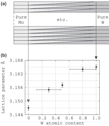
We have developed a process that allows us to fabricate achemical-gradient layer(CGL), i.e. a buffer layer whose composition varies continuously from one end to the other end of the wafer. In the present paper we focus on CGL made of mixtures of Mo and W, with bulk lattice parameters 3.147 ˚A and 3.165 ˚A, respectively. The process is the following.
Under the conditions detailed in section 2.1 we deposit sequentially W and Mo with the shape of opposite wedges, with an area of pure element on each side (Figure 6a). The growth temperature protocol is identical to that used for pure layers. The thickness of each bilayer is routinely 1 ˚A, although periods of 1 nm have been also used. The time required for the deposition of a full CGL is doubled with respect to a pure-element layer, and reaches approximately four hours. Extra time is indeed required to adjust the deposition parameters from one wedge to the next, consisting in closing the beam stop, changing of target and of laser focusing on the target, rotating the sample by 180◦ to alternate the direction of wedges, resetting the position of the mask, and opening the beam stop. This procedure is fully automated and controlled through a computer.
Upon this deposition procedure performed at moderate temperature a dual epitaxial relationship is evidence with RHEED, as with pure elements. Similarly to the case of W layers the minority twin can be completely eliminated upon annealing, provided that a dusting layer of Mo is deposited prior to the multilayer. After annealing the RHEED then displays a sharp 1×1 pattern. STM reveals a mono-atomic-stepped surface, similar to that of pure elements (Figure 2f). θ−2θ XRD was performed along the out-of-plane direction on several narrow slabs of these CGL. The out-of-plane lattice parameter varies indeed from that of W to that of Mo. It is expected that the in-plane lattice parameter undergoes also a linear variation.
Pure
Mo etc. Pure
W (a)
(b)
W atomic content
LatticeparameterÅ
3.144
0 0.2 0.4 0.6 0.8 1.0 3.150
3.156 3.162 3.168
Figure 6. (a) Schematic drawing of the geometry of a Chemical-Gradient Layer (CGL) (b) Out-of-plane lattice parameter of a Mo-W CGL. The vertical bars stand for experimental uncertainties, while the horizontal bars stand for the spread of composition on the slab measured related to the finite size of the area of CGL probed.
Although these CGL are fabricated by a multilayer process, a fine intermixing is expected owing to several arguments: the sub-monolayer period, the moderate deposition temperature, the small lattice misfit and the total solubility of W-Mo.
Accordingly we refer to these buffer layers assolid solutions throughout the manuscript.
Preliminary results suggest that the process works also finely for CGL made of Nb and Mo, two elements that also mix as solutions and form no alloys with specific stoichiometry in the bulk. In this case RHEED suggests a flat surface of high quality, with an in-plane lattice parameter continuously varying across the CGL. The process should be extended in the near future to (V,Mo) CGLs, with a view to spanning the in-plane lattice parameter of buffer solutions in the entire range [3.02−3.30 ˚A].
2.4. Pseudomorphic interfacial layer
The chemical nature of the interface is another key parameter in determining growth modes in epitaxy. Ideally, it is desirable to control the chemical nature of the supporting surface independently from the in-plane lattice parameter. To achieve this we have optimized a growth process to fabricate an ultrathin pseudomorphic layer of either Mo or W on the buffer layers previously described. We illustrate this procedure in this section for W deposited on Mo(8 nm). A wedge of W is deposited at RT on a flat Mo buffer layer, followed by annealing at increasing temperatures up to 700◦C. Auger
spectra of the low energy peaks of W and Mo were taken at RT after growth and after each step of annealing (Figure 7a-d). A quantitative analysis of the spectra in the range 130−240 eV suggested that upon annealing no change occurs in the relative intensity of both elements upon the entire range of thickness (Figure 7e). It is reasonable to assume that no intermixing occurs upon RT deposition, first because of the high temperature of melting of both elements, second because they have a similar atomic radius making exchange processes not clearly favorable, and third because (110) is a dense plane of the centered-cubic structure. Thus we assume that the spectra after deposition are a reference for a sharp interface. This is confirmed by the nearly exponential decay of the Mo intensity as a function of W thickness. Auger spectra do not show significant changes upon annealing, which suggests that the interface with Mo remains sharp, and that no diffusion of Mo to the free surface occurs. This point is essential to control the chemical nature of the interface. Finally we checked by STM that the surface resulting from annealing was flat at the atomic scale. For subsequent growth of Fe we used layers of thickness in the range 3−5 AL, where it is expected that the layers remain pseudomorphic thanks to the lattice misfit between Mo and W being smaller than 1%.
This point could no be checked directly due to the limited resolution of RHEED.
3. Overview of growth processes of Fe/bcc(110)
As recalled in the introduction, a large number of reports have already been made concerning the UHV growth modes of epitaxial Fe(110), mainly on W and more recently on Mo. Both cases were reported to be very similar, being of Stranski-Krastanov (SK) type with one single AL of wetting. Continuous films were successfully fabricated by RT deposition followed by moderate annealing, or by rising the temperature during deposition. Nanostructures were observed to form upon annealing at higher temperature or direct deposition at high temperatures.
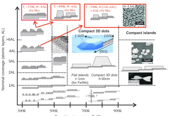
We have uncovered that the SK mode is in fact characterized by a bimodal distribution of islands (Figure 8). The first type consists of compact islands (i.e.
islands with all three dimensions of the same order of magnitude) that grow nearly homothetically during deposition, and whose shape can be understood on the basis of the Wulff-Kaischev geometrical construction (see [54] and included references). The second type consists of flat and thin islands (the ratio of lateral over vertical size can exceed 100), which display a nearly mono-disperse height that depends very little on deposition conditions nor on the lateral size of the islands. We already reported this bimodal growth mode for Fe/Mo(110)[35]. In the present manuscript we report it for the case of Fe/W(110), Fe on bcc(110) solid solutions, and as a function of the independently- controlled chemical nature of the interface. We also report the dependence of the bimodal growth features upon growth conditions, island density, shape and ratio of the two types. We have also tailored the growth of the flat islands to fabricate nanometers-thick stripes that are self-organized by step-decoration at the atomic steps of the buffer-layer. This is a fundamental advancement in self-organization as, up to
120 140 160 180 200 220 240 -800
-400 0
Mo: 0%
(a)
120 140 160 180 200 220 240 -800
-400 0
Mo: 19%
(b)
120 140 160 180 200 220 240 -1200
-800 -400 0 400
Mo: 44%
(c)
0.0 0.2 0.4 0.6 0.8 1.0
Amount of W deposited
AESintensityofMopeaks
20 Å
12 16
8 4 0
Annealing RT 300°C 500°C 700°C (e)
120 140 160 180 200 220 240 -2000
-1000 0 1000
Mo: 100%
(d)
Figure 7. (a-d) Selected AES spectra performed at RT in the range [120−250eV], of a wedged deposit of W on a smooth Mo(110) buffer layer (normalized arbitrary units). Experimental data (dots) are fitted in the range [130−240eV] with a linear combination of Mo and W reference spectra (line). The fitted contribution of the Mo reference spectrum is shown in inset (e) Intensity of the Mo spectrum as a function of the coverage of W, up to above 2.5 nm, and following various annealing
now and to our knowledge, only single- or double-AL stripes could be produced by step- decoration[55, 24, 23, 56]. We already reported the growth of such stripes on pure buffer layers[37, 38] and pure buffer layers covered with ultrathin pseudomorphic interfacial layers[39]. Here we also report the growth on buffer layers of solid solution to get a better insight in the physical origin underlying the bimodal growth. All these findings allow us to draw an enlarged panorama of growth processes of Fe on cc(110) surfaces as a function of amount of material deposited, temperatures of growth and possible annealing (Figure 9). On Figure 9 areas that had not been investigated quantitatively in the literature prior to our reports are illustrated with a picture of the resulting system.
The reason why these areas had been previously overlooked may come from the fact that studies on Fe(110) were already at the level of surface science when the interest in self- assembly arose. Thus studies were undertaken by STM, restricting the study to small lateral scales and amount of deposited material. Under these conditions it is not obvious to recognize the bimodal feature of growth, which on the other side is straightforward with AFM on a larger lateral scale. A discussion of the existing literature of the SK growth with respect to our data on the bimodal growth is proposed at the end of the manuscript, with a view to identifying whether the two types of islands had already been observed, however not identified as being of a different nature. Finally, although we evidenced no discrepancy between any of our data and the existing literature of Fe(110), concerning films or nanostructures, a difference of behavior between PLD (our technique) and MBE in the newly explored processes cannot be excluded.
4. Compact Fe islands
4.1. Overview
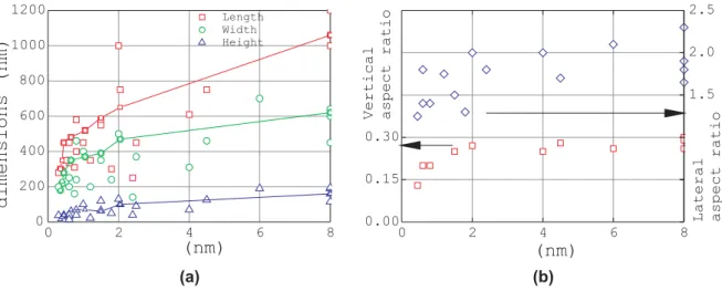
In the approximate range of temperature 325−575◦C compact Fe islands are formed upon deposition on Mo(110) and W(110) (Figure 8). The areal density decreases with temperature, from≈0.5µm−2at 325◦C to≈0.05µm−2at 575 K for a nominal thickness Θ ≈ 5 nm. This density increases very little in the range Θ = 1−10 nm, so that the mean dimensions of the dots scale roughly with √3
Θ, ending up in a range of length 100 nm−1µm (Figure 10). On this figure it can be seen that the distribution of mean size is significant from one sample to another. This suggests that the nucleation of dots does not depend solely on growth temperature but may also depend on extrinsic parameters such as step density and orientation[57] or residual contaminants at the surface.
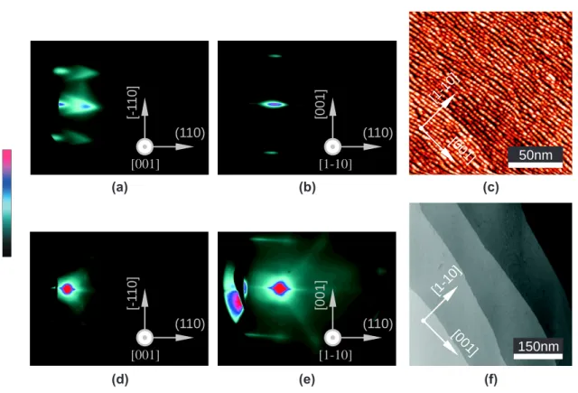
A closeup view of the dots reveals that they are facetted, and elongated along [001] (Figure 8b,d). The smoothness at the atomic scale of the top facet can be checked directly with AFM, with often no or only very few single atomic steps. No emerging screw dislocation has ever been observed either by this mean. The tilted facets are probed by RHEED in the form of tilted diffraction streaks, each perpendicular to one set of facets (Figure 11). The tilt angle of the facets is inferred directly from these
(a)
(c)
(b)
(d) [001]
[-110]
(110)
1 mm
1 mm [001]
[1-10]
[001]
[1-10]
1 mm
200nm
[001]
[-110]
(110)
200nm 1 mm
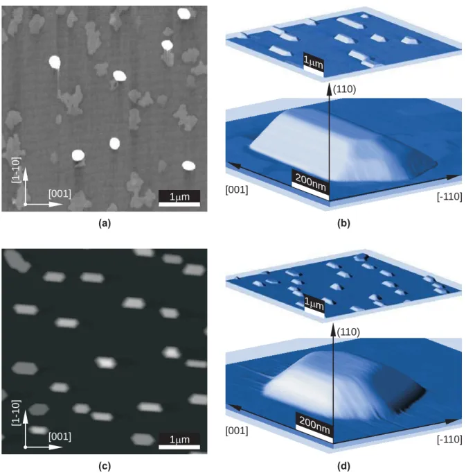
Figure 8. Illustration of the growth of Fe on (a-b) Mo(110) and (c-d) W(110).
(a) Deposition of Θ = 0.4 nm (early stages of growth) on Mo(110) at 450◦C The grey scale is chosen so as to highlight the bimodal growth mode (b) 3D view and closeup view of Fe/Mo(110) compact dots, deposited on Mo(110) at 500◦C, nominal thickness 2.5 nm (1:1 vertical scale) (c) Deposition of Θ = 2.5 nm on W(110) at 450◦C (d) 3D view and closeup view of Fe/W(110) compact dots as in (c).
Compact 3D dots
300K 500K 700K 900K
~750K ? 1AL
2AL 3AL 4AL
>6AL
Deposition temperature, T (K)S
Compact islands
Nominalcoverage(atomiclayers,AL)
T =700K, [2AL,6AL]
t=6AL (for Mo)
r Q
T <370K, >6AL (for Mo)
r Q T >400K, >6AL
(for Mo)
r Q
Flat islands t~1nm (for Fe/Mo)
Compact 3D dots t>30nm [-110]
[001]
(110)
Q~3.5AL
1 mm
5mm 2mm
500nm
Figure 9. Schematic overview of growth modes of Fe on Mo(110) and W(110) surfaces, as a function of temperature of deposition and amount of Fe deposited. The output of annealing is displayed in rectangles. The growth modes for which we reported the first contribution are illustrated with a picture
0 2 4 6 8
0 200 400 600 800 1000
1200 Length
Width Height
(nm)
dimensions(nm) Vertical aspectratio Lateral aspectratio
0 2 4 6 8
0.00 0.15 0.30
(nm)
1.5 2.0 2.5
(a) (b)
Figure 10. (a) Distribution and increase of the dimensions of compact dots for a series of samples grown at 450◦C, versus nominal thickness Θ. The full lines stand for one selected sample (b) Vertical (squares) and lateral (diamonds) aspect ratio depending on growth temperature.
patterns, much more reliably than with AFM were tip shading effects may arise for such steep slopes. The sharpness of the streaks suggests the smoothness at the atomic scale of the facets. The values of the angles of the facets are analyzed quantitatively in the following paragraph. On Figure 11 notice also the doublets of horizontal streaks, revealing the in-plane lattice parameters of both the substrate and Fe, arising from pseudomorphic areas and top facets of Fe islands, respectively. The doublets are better seen for Fe/W(110) (Figure 11d-f), where it is also clear that the intercept of the tilted streaks occurs on the horizontal streaks associated with Fe, as expected. XRD was performed in the θ −2θ geometry, showing that the lattice parameter of Fe in the dots equals that of bulk within better than 0.1 %. The crystalline coherence length, extracted from the analysis of the peak width using the Scherrer formula, equals the mean thickness of the dots. Owing first to the size distribution between dots, second to the distribution of local heights in each dot resulting from the tilted facets, this peak does no display side oscillations like for smooth films in Figure 4.
4.2. Wulff-Kaishev construction for Fe(110) dots
In the view of the above topographic and structural data, self-assembled Fe(110) dots can be considered to be elastically relaxed single crystals. The shape of such crystals at equilibrium on a supporting surface is described by the Wulff-Kaishev construction (Figure 13a):
γi
hi
= (γint−γS) hint
= Constant (1)
whereγi is the free energy of facetsi of a given family of crystallographic planes of the material,γS is that of the free surface of the substrate, andγint is the interfacial free energy[54]. From the calculated surface energies[3], the free surfaces of a free-standing Fe crystal are expected to be mainly of type{110}and{100}, with secondary{211}and {310} facets. RHEED is consistent in revealing these four types of facets, plus {332} along the electron azimuth < 1−10 > (Figure 11). Notice however that not all dots display facets other than {001} and {110}. Finally, sharp edges are scarcely observed by AFM. It is not clear whether this stems from the rounded shape of the tip at the scale of a few tens of nanometers, or whether edges are really rounded.
The schematic shape of both types of facetted crystals are shown in Figure 14. For comparison notice in Figure 11 that for [1−10] and [1−11] azimuths facets with the highest angle arise for Fe/Mo however not for Fe/W. This is explained by the fact that Fe/W crystals are flatter than Fe/Mo crystals so that steep facets are not involved, see next paragraph where the aspect ratios of the dots are analyzed quantitatively. For this analysis we introduce two parameters to characterize the islands: the lateral aspect ratio r = L/w and the vertical aspect ratio η = h/w where L, w and h are respectively the base full length, the base full width and the height (Figure 13b). These aspect ratios can be derived from Eq. (1), see Appendix I. The calculated variation of r andη versus γint are shown on Figure 15, assuming γS =γ{110}, see the discussion at the end of this
(a)
(d)
(b)
(e)
(c)
(f) (110)
[-110]
[001]
(110)
[001]
[1-10]
(110)
[-112]
[1-11]
(110)
[-110]
[001]
(110)
[001]
[1-10]
(110)
[-112]
[1-11]
Figure 11. RHEED patterns of compact Fe(110) dots deposited on (a-c) Mo(110) and (d-f) W(110). The sample lies on the left of the patterns, with the mean surface vertical. The azimuths are (a,d) [001], (b,e) [1−10], (c,f) [1−11]. The plane of incidence is indicated with a white arrow pointing on the reflected beam. The sample is rotated a few degrees off these azimuths for all images, because this allows to better evidence the tilted streaks arising from facets. The facets evidenced are of type (a){200}and weaker{310} (b){112}and weaker{332}(c) {110}and weaker{211}(d){200}and {310}(e){332}(f) {420}(see Appendix 2).
A
0 800 nm 1600
0 0.2 0.4 µm
B
0 800 nm 1600
0 0.2 0.4 µm
C
0 800 nm 1600
0 0.2 0.4 0.6 0.8 µm
400nm
A
C
B
Figure 12. Experimental cross-sections averaged laterally, performed on the dot shown in Figure 8b, labelled A, B, C on the AFM picture. Thin straight lines highlight the facets on the cross-sections.
(010) (110) (100)
(110) [001]
[1-10]
L
w h
(a) (b)
g
jg
ig
inthint
h
iFigure 13. (a) Notations used for the Wulff-Kaishev theorem. The dashed surface stands for the supporting surface and the darker part of the crystal is the supported crystal. (b) Definition of the full widthw, heighthand full length L, which can also be defined if the dot does not display symmetric facets, as illustrated here.
section. The variation ofηdoes not depend on the number of facets considered excepted for very thin dots where {310} facets come into play (see Figure 14). On the reverse for any thickness the length of the dot is reduced upon the consideration of additional facets, so that not all curves for r are superimposed.
4.3. Experimental determination of interfacial energies
The size and aspect ratios of dots on a given sample are distributed, see Figure 8. The mean experimental values ofrandηare nearly independent on growth temperature (not
[001]
[-110]
(110) (g) (h)
(a) (b) (c)
(d) (e) (f)
Figure 14. Wulff (a-c) and Wulff-Kaishev (d-h) constructions. (a-f) are drawn based on the values of surface energy computed by Vitos[3]: γ{110} = 2.430 J/m2; γ{001} = 2.222 J/m2; γ{211} = 2.589 J/m2; γ{310} = 2.393 J/m2. For (g) and (h) γ{110}, γ{001} and γint have been reduced by 2.5 % and 5 %, respectively. (d-h) are drawn based on the interfacial energy determined experimentally: γint = 0.65 J/m2. The facets taken into account are{001}and{110}in (a,d), adding{211}in (b,e) and {310}in (c,f-h). {332}facets are not shown because their energy was not reported by Vitos, although these facets are evidenced by RHEED in the experiments (Figure 8).
0 0.2 0.4 0.6 0.8 1 1.2 1
2 3
0 0.5 r L w= /
h=h/w
g
int (J/m )2 W MoW
Mo
With facets:
{110} & {100}
{110}, {100}
& {310}
{110}, {100}, {310} & {211}
0.0 1.0 2.0
Figure 15. Lateralr=L/wand verticalη=h/laspect ratios of supported Fe(110) dots depending on the interfacial energyγint. The calculations were made considering two, three and four types of facets, and assuming γS = γ{110} (see Appendix I).
The vertical size of the rectangles stands for the spread of experimental aspect ratios observed for Fe/W (left) and Fe/Mo (right).
shown in this manuscript) and nominal thickness (Figure 10), as expected for an equilibrium situation resulting solely from the minimization of surface energy, with a vanishing elastic energy. We find η ≃ 0.25 and r ≃ 1.6 for Fe/Mo, and η ≃ 0.1 and r ≃ 2.7 for Fe/W. These values and their experimental distribution are reported on Figure 15 on the y axis, defining segments. The calculated curves of aspect ratios were used to convert these y-segments in segments along the x axis, defining the rectangles shown in the figure. This determines the range of interfacial energy values compatible with the observations. The relevance of the Wulff-Kaishev construction here is indicated by the overlap of the range of interfacial energies compatible with both the observed lateral and vertical aspect ratios. We deduce γint,Mo = 0.65±0.15 J.m−2 and γint,W = 0.10±0.05 J.m−2. The most probable values were derived based mostly on the value of η. Indeed, first the experimental distribution is found to be larger for r than for η, second the mean value of r was found to vary slightly more then during growth than that of η (Figure 10b). The experimental mean values for r and η have also been measured for combinations of buffer layer and pseudomorphic interfacial layers, i.e. Mo/W and W/Mo. It was found that γint is related to the chemical nature of the interface or interfacial layer, not on the in-plane lattice parameter imposed by the underlaying buffer layer. These facts are discussed later. In the future these studies should be extended to CGL buffer with Mo or W interfacial layers, so that the contribution of dislocations and elastic energy on effective interfacial energies is derived.
4.4. Limits of the temperature range for the growth of compact dots
The in-plane shape of the dots becomes more and more irregular when the growth temperature is reduced below ≈ 350◦C, and the tilted facets tend to disappear. At
the opposite range, when the growth temperature is raised above ≈ 500◦C the tilted facets are still well defined, but the aspect ratios become more and more distributed. The distribution ofηbroadens less than that ofr. Thus, the optimum range of temperatures for growing faceted dots with a moderate distribution of aspect ratios is 350◦C−500◦C.
It will be shown in sec. 5 for Fe/Mo that at still higher temperatures the SK growth is initiated with flat dots and not with compact dots.
4.5. Changes of shape induced by surfactant-mediated growth
Surfactants are used in epitaxial growth to promote a layer-by-layer growth mode like with Pb with Co/Cu(111)[58] or O for Fe(001)[59]. Kinetic effects are often identified as the leading effect promoting layer-by-layer growth[60], by lowering diffusion energies.
A side effect is the lowering of surface energies when surfactants are present. The ratio of the different surface energies might be also changed, which should a modification of the shape of crystals.
We have observed a surfactant effect of Sm on Fe(110) dots. Upon deposition from a SmFe2 compound target, we have observed in a narrow range of temperatures around 450◦C the formation of hut-shaped dots (Figure 16a)[61]. XRD revealed that the dots are made of pure Fe relaxed to the bulk lattice parameter with no indication of Sm or any SmFe compounds. This can be explained by the low evaporation temperature of Sm under UHV,≈200◦C, so that Sm re-evaporates from the surface and does not contribute to the formation of SmFe compounds, for which the present temperatures are too low.
Auger spectra revealed that a weak amount of Sm remains at the surface, probably one atomic layer, that significantly lowers the surface energies of Fe and therefore whose evaporation is hindered[62]. These hut-shaped dots were similarly obtained after the deposition of pure Fe on∼1 AL Sm on Mo(110) at 475◦C (Figure 16b), supporting the aforementioned growth mechanism using a SmFe2 target and confirming the surfactant effect of Sm.
It is obvious that the surface energies of the various bcc-Fe facets are not decreased in a proportional way, as the huts are elongated along [110] and display {111}facets on the sides and{001}facets at both ends. No{110}facets are visible . A na¨ıve explanation why{111}facets are favored to{110}come from hexagonal symmetry of both Mo{111} and Sm {0001}, and also the lattice mismatch being smaller for Sm(0001)/Mo(111) than for Sm(0001)/Mo(110), respectively 12 % versus 15 %. The real picture is more complicated as the valence of Sm depends sensitively on strain and on the number of ALs deposited[62, 63, 64, 65].
Let us add a word about surface contamination by residual gases. In the rare cases where the level of vacuum was poor during deposition, i.e. typically 1×10⁻⁹Torr, the shape of the dots was altered: elongated dots were formed, with their height significantly increased at both ends in a shape of dome (Figure 16c). As these domes remain located at the end of the dots, whose length increases during the course of growth, it is likely that they move along the dot while growth proceeds. The composition of the surface
![Figure 3. RHEED patterns on a grooved surface arising upon deposition of W(110) at 100 ◦ C, along the (a) [001] azimuth (b) same as a, misoriented by ◦ 1 away from [001]](https://thumb-eu.123doks.com/thumbv2/1bibliocom/472538.75572/10.892.106.794.109.470/figure-patterns-grooved-surface-arising-deposition-azimuth-misoriented.webp)
![Figure 7. (a-d) Selected AES spectra performed at RT in the range [120 − 250eV], of a wedged deposit of W on a smooth Mo(110) buffer layer (normalized arbitrary units)](https://thumb-eu.123doks.com/thumbv2/1bibliocom/472538.75572/16.892.206.678.118.842/figure-selected-spectra-performed-wedged-deposit-normalized-arbitrary.webp)