HAL Id: tel-00838736
https://tel.archives-ouvertes.fr/tel-00838736
Submitted on 26 Jun 2013
HAL is a multi-disciplinary open access archive for the deposit and dissemination of sci- entific research documents, whether they are pub- lished or not. The documents may come from teaching and research institutions in France or abroad, or from public or private research centers.
L’archive ouverte pluridisciplinaire HAL, est destinée au dépôt et à la diffusion de documents scientifiques de niveau recherche, publiés ou non, émanant des établissements d’enseignement et de recherche français ou étrangers, des laboratoires publics ou privés.
High Frequency MEMS Sensor for Aero-acoustic Measurements
Zhijian J. Zhou
To cite this version:
Zhijian J. Zhou. High Frequency MEMS Sensor for Aero-acoustic Measurements. Micro and nan- otechnologies/Microelectronics. Université de Grenoble, 2013. English. �NNT : �. �tel-00838736�
THÈSE
Pour obtenir le grade de
DOCTEUR DE L’UNIVERSITÉ DE GRENOBLE
Spécialité : NANO ELECTRONIQUE NANO TECHNOLOGIES
Arrêté ministériel : 7 août 2006
Et de
DOCTEUR DE THE HONG KONG UNIVERSITY OF SCIENCE AND TECHNOLOGY
Spécialité : ELECTRONIC AND COMPUTER ENGINEERING
Présentée par
«Zhijian ZHOU»
Thèse dirigée par «Libor RUFER» et codirigée par «Man WONG»
préparée au sein du Laboratoire TIMA
dans l'École Doctorale Electronique, Electrotechnique, Automatique et Traitement du Signal
et Electronic and Computer Engineering Department
Microcapteurs de Hautes
Fréquences pour des Mesures en Aéroacoustique
Thèse soutenue publiquement le «01/21/2013», devant le jury composé de :
M. David COOK
Professeur Associé, Hong Kong University of Science & Technology, Président
M. Philippe, BLANC-BENON
Directeur de Recherche, CNRS, Ecole Centrale de Lyon, Rapporteur
M. Philippe COMBETTE
Professeur, Université Montpellier II, Rapporteur
M. Skandar BASROUR
Professeur, Université Joseph Fourier, Grenoble, Examinateur
Mme Wenjing YE
Professeur Associé, Hong Kong University of Science & Technology, Examinateur
M. Levent YOBAS
Professeur Assistant, Hong Kong University of Science & Technology, Examinateur M. Man WONG
Professeur, Hong Kong University of Science & Technology, Co-Directeur de thèse
High Frequency MEMS Sensor for Aero-acoustic Measurements
By
ZHOU, Zhijian
A Thesis Submitted to
The Hong Kong University of Science and Technology in Partial Fulfillment of the Requirements for
the Degree of Doctor of Philosophy
in the Department of Electronic and Computer Engineering and
Université de Grenoble
in Partial Fulfillment of the Requirements for the Degree of Docteur de l’ Université de Grenoble
in the Ecole Doctorale Electronique, Electrotechnique, Automatique & Traitement du Signal
February 2013, Hong Kong
Authorization
I hereby declare that I am the sole author of the thesis.
I authorize the Hong Kong University of Science and Technology and Université de Grenoble to lend this thesis to other institutions or individuals for the purpose of scholarly research.
I further authorize the Hong Kong University of Science and Technology and Université de Grenoble to reproduce the thesis by photocopying or by other means, in total or in part, at the request of other institutions or individuals for the purpose of scholarly research.
___________________________________________
ZHOU, Zhijian
February 2013
High Frequency MEMS Sensor for Aero-acoustic Measurements
By
ZHOU, Zhijian
This is to certify that I have examined the above Ph.D thesis and have found that it is complete and satisfactory in all respects, and that any and all revisions required by the thesis
examination committee have been made.
___________________________________________
Prof. Man WONG
Department of Electronic and Computer Engineering, HKUST, Hong Kong Thesis Supervisor
___________________________________________
Prof. Libor RUFER Université de Grenoble, France
Thesis Co-Supervisor
___________________________________________
Prof. David COOK
Department of Economics, HKUST, Hong Kong Thesis Examination Committee Member (Chairman)
___________________________________________
Prof. Skandar BASROUR
Université de Grenoble, Grenoble, France Thesis Examination Committee Member
___________________________________________
Prof. Wenjing YE
Department of Mechanical Engineering, HKUST, Hong Kong Thesis Examination Committee Member
___________________________________________
Prof. Levent YOBAS
Department of Electronic and Computer Engineering, HKUST, Hong Kong Thesis Examination Committee Member
___________________________________________
Prof. Ross MURCH
Department of Electronic and Computer Engineering, HKUST, Hong Kong Department Head
Department of Electronic and Computer Engineering The Hong Kong University of Science and Technology
February 2013
Acknowledgments
I would like to give my deepest appreciation first and foremost to Professor Man WONG and Professor Libor RUFER, my supervisors, for their constant encouragement, guidance and support though my Ph.D study at HKUST and Université de Grenoble. Without their consistent and illuminating instructions, this thesis could not have reached its present form.
Also, I want to thank Professor David COOK for agreeing to chair my thesis examination and Professor Skandar BASROUR, Dr. Philippe BLANC-BENON, Professor Philippe COMBETTE, Professor Wenjing YE and Professor Levent YOBAS for agreeing to serve as members of my thesis examination committee.
I would like to thank Dr. Sébastien OLLIVIER, Dr. Edouard SALZE and Dr. Petr YULDASHEV, who are from Laboratoire de Mécanique des Fluides et d'Acoustique (LMFA, Ecole Centrale de Lyon) and Dr. Olivier LESAINT, who is from Grenoble Génie Electrique (G2E lab); the group of Professor Pascal NOUET, who is from Laboratoire d'Informatique, de Robotique et de Microélectronique de Montpellier (LIRMM, l'Université Montpellier 2); and Dr. Didace EKEOM, who is from the Microsonics company (http://www.microsonics.fr/), for their help in guiding the microphone dynamic calibration experiment, offering the first prototype of the amplification card and teaching the ANSYS simulation software under the project Microphone de Mesure Large Bande en Silicium pour l'Acoustique en Hautes Fréquences (SIMMIC), which is financially supported by French National Research Agency (ANR) Program BLANC 2010 SIMI 9.
I have appreciated the help of the staffs from the nanoelectronics fabrication facility (NFF) and materials characterization and preparation facility (MCPF) of HKUST and the technicians from the Department of Electronic and Computer Engineering and the Department of Mechanical Engineering of HKUST. Also I have appreciated the help of the engineers from the campus d'innovation pour les micro et nanotechnologies (MINATEC).
Through my Ph.D study period, much assistance has been given by my colleagues and friends at HKUST. I appreciate their kindly help and support and would like to thank them all, especially Ruiqing ZHU, Zhi YE, Thomas CHOW, Dongli ZHANG, Parco WONG, Zhaojun LIU, Shuyun ZHAO, He LI, Fan ZENG and Lei LU.
During my periods of stay in Grenoble, many friends helped me to quickly settle in and integrate into the French culture. I would like to thank them all, especially Hai YU, Wenbin YANG, Ke HUANG, Yi GANG, Richun FEI, Nan YU, Zuheng MING, Haiyang DING, Weiyuan NI, Hao GONG, Zhongyang LI, Bo WU, Josue ESTEVES, Yoan CIVET, Maxime DEFOSSEUX, Matthieu CUEFF and Mikael COLIN.
Last but not least, I devote my deepest gratitude to my parents for their immeasurable support over the years.
To my family
Table of Contents
High Frequency MEMS Sensor for Aero-acoustic Measurements ...ii
Authorization...iii
Acknowledgments... vi
Table of Contents ... ix
List of Figures ...xii
List of Tables ...xvii
Abstract ...xviii
Résumé ... xx
Publications ... xxi
Chapter 1: Introduction ... 1
1.1 Introduction of the Aero-Acoustic Microphone ... 1
1.1.1 Definition of Aero-Acoustics and Research Motivation ... 1
1.1.2 Wide-Band Microphone Performance Specifications... 3
1.2 A Comparative Study of Current State-of-the-art MEMS Capacitive and Piezoresistive Microphones... 5
1.3 Existing Fabrication Techniques for Piezoresistive Aero-Acoustic Microphones... 10
1.4 Summary ... 12
1.5 References ... 13
Chapter 2: MEMS Sensor Design and Finite Element Analysis... 16
2.1 Key Material Properties ... 16
2.1.1 Diaphragm Material Residual Stress... 16
2.1.2 Diaphragm Material Density and Young’s Modulus... 20
2.2 Design Considerations... 24
2.3 Mechanical Structure Modeling ... 28
2.4 Summary ... 36
2.5 References ... 37
Chapter 3: Fabrication of the MEMS Sensor ... 38
3.1 Review of Metal-induced Laterally Crystallized Polycrystalline Silicon Technology38
3.2 Surface Micromachining Process... 44
3.2.1 Sacrificial Materials and Cavity Formation Technology ... 44
3.2.2 Contact and Metallization Technology... 54
3.2.3 Details of Fabrication Process Flow... 58
3.3 Silicon Bulk Micromachining Process... 65
3.3.1 Comparison of Bulk Silicon Wet Etching and Dry Etching Techniques... 65
3.3.2 Details of Fabrication Process Flow... 68
3.4 Summary ... 72
3.5 References ... 73
Chapter 4: Testing of the MEMS Sensor... 77
4.1 Sheet Resistance and Contact Resistance... 77
4.2 Static Point-load Response... 80
4.3 Dynamic Calibration ... 84
4.3.1 Review of Microphone Calibration Methods... 84
4.3.1.1 Reciprocity Method... 84
4.3.1.2 Substitution Method ... 86
4.3.1.3 Pulse Calibration Method... 88
4.3.2 The Origin, Characterization and Reconstruction Method of N Type Acoustic Pulse Signals ... 90
4.3.2.1 The Origin and Characterization of the N-wave ... 91
4.3.2.2 N-wave Reconstruction Method... 96
4.3.3 Spark-induced Acoustic Response ... 99
4.3.3.1 Surface Micromachined Devices ... 102
4.3.3.2 Bulk Micromachined Devices... 105
4.4 Sensor Array Application as an Acoustic Source Localizer... 108
4.5 Summary ... 116
4.6 References ... 117
Chapter 5: Summary and Future Work... 119
5.1 Summary ... 119
5.2 Future Work... 122
5.3 References ... 123
Appendix I: Co-supervised Ph.D Program Arrangement... 124
Appendix II: Extended Résumé ... 125
List of Figures
Figure 1.1: Schematic of a typical capacitive microphone. ... 6
Figure 1.2: Schematic of a typical piezoresistive microphone... 7
Figure 1.3: Process flow of the fusion bonding technique... 10
Figure 1.4: Process flow of the low temperature direct bonding with smart-cut technique. ... 11
Figure 2.1: Bending of the film-substrate system due to the residual stress... 17
Figure 2.2: Layout of a single die. ... 18
Figure 2.3: Layout of the rotational beam structure... 19
Figure 2.4: Microphotography of two typical rotational beams after releasing... 20
Figure 2.5: Layout of the doubly-clamped beams... 21
Figure 2.6: Resonant frequency measurement setup... 22
Figure 2.7: Typical measurement result of the laser vibrometer. ... 22
Figure 2.8: Surface micromachining technique. ... 24
Figure 2.9: Bulk micromachining technique... 25
Figure 2.10: Schematic of the microphone physical structure using the surface micromachining technique. ... 27
Figure 2.11: Schematic of the microphone physical structure using the bulk micromachining technique. ... 27
Figure 2.12: Layout of a fully clamped square diaphragm. ... 29
Figure 2.13: ANSYS first mode resonant frequency simulation of a square diaphragm. ... 30
Figure 2.14: Sensor analogies. ... 31
Figure 2.15: Mechanical frequency response of a square diaphragm. ... 32
Figure 2.16: Layout of a beam supported diaphragm (reference resistors are not shown). ... 33
Figure 2.17: Cross-sectional view of coupled acoustic-mechanical FEA model... 34
Figure 2.18: Mechanical frequency response of a beam supported square diaphragm... 35
Figure 3.1: Ni/Si equilibrium free-energy diagram... 43
Figure 3.2: Cross-sectional view of microphone before release. ... 45
Figure 3.3: Cross-sectional view of microphone after first TMAH etching. ... 45
Figure 3.4: Amorphous silicon etching rate at 60℃ TMAH... 45
Figure 3.5: Cross-sectional view of microphone after BOE etching. ... 46
Figure 3.6: Cross-sectional view of microphone after second TMAH etching... 46
Figure 3.7: Sacrificial oxide layer etching profile... 47
Figure 3.8: Sacrificial oxide layer lateral etching rate. ... 47
Figure 3.9: Detail of the etching profile due to the dimple mold... 49
Figure 3.10: AFM measurement of the substrate sc-silicon etching profile due to the dimple mold in room temperature TMAH solution. ... 52
Figure 3.11: Silicon lateral etching rate of the TMAH solution at room temperature. ... 53
Figure 3.12: Silicon vertical etching rate of the TMAH solution at room temperature. ... 53
Figure 3.13: Metal peel-off due to large residual stress. ... 54
Figure 3.14: Reverse trapezoid shape of the dual tone photoresist... 55
Figure 3.15: Cross-sectional view of microphone after Ti sputtering... 56
Figure 3.16: Cross-sectional view of microphone after the silicidation process. ... 56
Figure 3.17: Contact resistance comparison (different HF pre-treatment time). ... 57
Figure 3.18: Contact resistance comparison (with/without silicidation)... 57
Figure 3.19: Thermal oxide hard mask. ... 58
Figure 3.20: Photolithography for dimple mold... 58
Figure 3.21: Etching of thermal oxide hard mask... 58
Figure 3.22: Etching of the reverse dimple mold... 58
Figure 3.23: Deposition of sacrificial layers. ... 59
Figure 3.24: Diaphragm area photolithography. ... 59
Figure 3.25: Diaphragm area etching... 59
Figure 3.26: Piezoresistor material deposition... 60
Figure 3.27: Define piezoresistor shape... 60
Figure 3.28: LTO deposition. ... 61
Figure 3.29: Open induce hole. ... 61
Figure 3.30: Ni evaporation. ... 61
Figure 3.31: Microphotography of amorphous silicon after re-crystallization. ... 61
Figure 3.32: Remove Ni and high temperature annealing. ... 61
Figure 3.33: Boron doping and activation... 62
Figure 3.34: Second low stress nitride layer deposition... 62
Figure 3.35: Open contact hole. ... 63
Figure 3.36: Open release hole... 64
Figure 3.37: Metallization after lift-off process. ... 64
Figure 3.38: Microphotography of a wide-band high frequency microphone fabricated using the surface micromachining technique... 64
Figure 3.39: Etching profile of the KOH/TMAH solutions. ... 66
Figure 3.40: Top view of an arbitrary backside opening etching shape... 67
Figure 3.41: Diaphragm layers deposition. ... 68
Figure 3.42: Piezoresistor forming... 68
Figure 3.43: Piezoresistor protection and backside hard mask deposition. ... 69
Figure 3.44: Metallization. ... 69
Figure 3.45: Diaphragm area patterning. ... 70
Figure 3.46: Cross-sectional view of the microphone device after dry etching release... 70
Figure 3.47: Microphotography of a wide-band high frequency microphone fabricated using bulk micromachining technique. ... 70
Figure 3.48: Cross-sectional view microphotography of the cut die edge... 71
Figure 4.1: Layout of the Greek cross structure... 77
Figure 4.2: Layout of the Kelvin structure... 78
Figure 4.3: Static measurement setup... 80
Figure 4.4: Cross-sectional view of the probe applying the point-load. ... 80
Figure 4.5: Wheatstone bridge configuration... 81
Figure 4.6: Typical measurement result with a diaphragm length of 115μm and thickness of 0.5μm (fabricated using the surface micromachining technique). ... 81
Figure 4.7: Typical measurement result with a diaphragm length of 210μm and thickness of 0.5μm (fabricated using the bulk micromachining technique)... 82
Figure 4.8: Point-load vs. displacement relationships of sensors fabricated using two different micromachining techniques... 83 Figure 4.9: Equivalent pressure vs. displacement relationships of sensors fabricated using two
different micromachining techniques... 83
Figure 4.10: Principle of Pressure Reciprocity Calibration. The three microphones (A, B and C) are coupled two at a time together by the air (or gas) enclosed in a cavity while the three ratios of output voltage and input current are measured. Each ratio equals the Electrical Transfer Impedance valid for the respective pair of microphones... 86
Figure 4.11: Pulse signals and their corresponding spectrums. ... 89
Figure 4.12: An ideal N-wave in 10 μs duration and its corresponding frequency spectrum. . 90
Figure 4.13: N-wave near projectile (a) Cone-cylinder, (b) Sphere... 91
Figure 4.14: N-wave generation process... 92
Figure 4.15: Schematic of the shock tube. ... 93
Figure 4.16: High voltage capacitor discharge scheme... 94
Figure 4.17: Schematic of an ideal N-wave. ... 96
Figure 4.18: Real N-wave shape. ... 97
Figure 4.19: Shadowgraph experiment setup (1. spark source, 2. microphone in a baffle, 3. nanolight flash lamp, 4 focusing lens, 5. camera, 6. lens). ... 98
Figure 4.20: Comparison between the optically measured rise time and the predicted rise time by using the acoustic wave propagation at different distances from the spark source... 98
Figure 4.21: Schematic of the amplifier. ... 100
Figure 4.22: Frequency response of the amplification card. ... 100
Figure 4.23: Spark calibration test setup... 101
Figure 4.24: Baffle design... 101
Figure 4.25: Typical spark measurement result of a microphone sample fabricated using the surface micromachining technique (3V DC bias, with amplification gain 1000 and source to microphone distance is 10cm)... 103
Figure 4.26: FFT single-sided amplitude spectra of the measured signals from a surface micromachined microphone and from optical method. ... 103
Figure 4.27: Frequency response of the calibrated microphone (3V DC bias, with amplification gain 1000, averaged signal), compared with FEA result. ... 104
Figure 4.28: Acoustic short circuit induced leakage pressure Ps. ... 104 Figure 4.29: Typical spark measurement result of a microphone sample fabricated using the
bulk micromachining technique (3V DC bias, with amplification gain 1000 and source to
microphone distance is 10cm)... 105
Figure 4.30: FFT single-sided amplitude spectra of the measured signals from a bulk micromachined microphone and from optical method. ... 105
Figure 4.31: Frequency response of the calibrated microphone (3V DC bias, with amplification gain 1000, averaged signal), compared with lumped-element modeling result. ... 106
Figure 4.32: Comparison of the spark measurement results of microphones fabricated by two different techniques (spark source to microphone distance is 10cm). ... 107
Figure 4.33: Comparison of the frequency responses of microphones fabricated by two different techniques. ... 107
Figure 4.34: Cartesian coordinate system for acoustic source localization. ... 108
Figure 4.35: Sensor array coordinates... 109
Figure 4.36: Sound velocity calibration setup... 110
Figure 4.37: Sound velocity extrapolation. ... 110
Figure 4.38: Acoustic source localization setup... 111
Figure 4.39: GUI initialization for sound velocity input... 111
Figure 4.40: Localization GUI main window... 112
Figure 4.41: Localization test Z coordinate system. ... 113
Figure 4.42: Sound source position definition. ... 113
Figure 4.43: Coordinates comparisons between the pre-measured values and the calculated values, (a): X coordinates; (b) Y coordinates and (c) Z coordinates... 114
Figure 4.44: Y coordinates differences between the pre-measured values and the calculated values due to unlevel ground surface. ... 115
List of Tables
Table 1.1: Current state-of-the-art of developed MEMS aero-acoustic microphones. ... 8
Table 1.2: Scaling properties of MEMS microphones. ... 9
Table 1.3: Scaling example. ... 9
Table 2.1: Curvature method measurement parameters and results... 17
Table 2.2: Rotational beam design parameters... 19
Table 2.3: Dimension of different beams (length×width [μm×μm])... 21
Table 2.4: First mode resonant frequencies of different beams (1μm thick)... 23
Table 2.5: Square diaphragm modeling parameters. ... 29
Table 2.6: Variable analogy. ... 30
Table 2.7: Element analogy. ... 31
Table 2.8: Coupled acoustic-mechanical modeling parameters. ... 35
Table 4.1: Summary of different microphone calibration methods... 90
Table 4.2: Distance between table surface and ground surface at different positions... 115
Table 5.1: Comparisons of current work and state-of-the-art. ... 121
High Frequency MEMS Sensor for Aero-acoustic Measurements
By
ZHOU, Zhijian
Electronic and Computer Engineering The Hong Kong University of Science and Technology
and
Ecole Doctorale Electronique, Electrotechnique, Automatique & Traitement du Signal Université de Grenoble
Abstract
Aero-acoustics, a branch of acoustics which studies noise generation via either turbulent fluid motion or aerodynamic forces interacting with surfaces, is a growing area and has received fresh emphasis due to advances in air, ground and space transportation. While tests of a real object are possible, the setup is usually complicated and the results are easily corrupted by the ambient noise. Consequently, testing in relatively tightly-controlled laboratory settings using scaled models with reduced dimensions is preferred. However, when the dimensions are reduced by a factor of M, the amplitude and the bandwidth of the corresponding acoustic waves are increased by 10logM in decibels and M, respectively. Therefore microphones with a bandwidth of several hundreds of kHz and a dynamic range covering 40Pa to 4kPa are needed for aero-acoustic measurements.
Micro-Electro-Mechanical-system (MEMS) microphones have been investigated for more than twenty years, and recently, the semiconductor industry has put more and more concentration on this area. Compared with all other working principles, due to their scaling
characteristic, piezoresistive type microphones can achieve a higher sensitivity bandwidth (SBW) product, and in turn they are well suited for aero-acoustic measurements. In this thesis, two metal-induced-lateral-crystallized (MILC) polycrystalline silicon (poly-Si) based piezoresistive type MEMS microphones are designed and fabricated using surface micromachining and bulk micromachining techniques, respectively. These microphones are calibrated using an electrical spark generated shockwave (N-wave) source. For the surface micromachined sample, the measured static sensitivity is 0.4μV/V/Pa, dynamic sensitivity is 0.033μV/V/Pa and the frequency range starts from 100kHz with a first mode resonant frequency of 400kHz. For the bulk micromachined sample, the measured static sensitivity is 0.28μV/V/Pa, dynamic sensitivity is 0.33μV/V/Pa and the frequency range starts from 6kHz with a first mode resonant frequency of 715kHz.
Résumé
L’aéroacoustique est une filière de l'acoustique qui étudie la génération de bruit par un mouvement fluidique turbulent ou par les forces aérodynamiques qui interagissent avec les surfaces. Ce secteur en pleine croissance a attiré des intérêts récents en raison de l’évolution de la transportation aérienne, terrestre et spatiale. Alors que les tests sur un objet réel sont possibles, leur implantation est généralement compliquée et les résultats sont facilement corrompus par le bruit ambiant. Par conséquent, les tests plus strictement contrôlés au laboratoire utilisant les modèles de dimensions réduites sont préférables. Toutefois, lorsque les dimensions sont réduites par un facteur de M, l'amplitude et la bande passante des ondes acoustiques correspondantes se multiplient respectivement par 10logM en décibels et par M.
Les microphones avec une bande passante de plusieurs centaines de kHz et une plage dynamique couvrant de 40Pa à 4 kPa sont ainsi nécessaires pour les mesures aéroacoustiques.
Les microphones MEMS ont été étudiés depuis plus de vingt ans, et plus récemment, l'industrie des semiconducteurs se concentre de plus en plus sur ce domaine. Par rapport à tous les autres principes de fonctionnement, grâce à la caractéristique de minimisation, les microphones de type piézorésistif peuvent atteindre une bande passante de sensibilité (SBW) plus élevée et sont ainsi bien adaptés pour les mesures aéroacoustiques. Dans cette thèse, deux microphones MEMS de type piézorésistif à base de silicium polycristallin (poly-Si) latéralement cristallisé par l’induction métallique (MILC) sont conçus et fabriqués en utilisant respectivement les techniques de microfabrication de surface et de volume. Ces microphones sont calibrés à l'aide d'une source d’onde de choc (N-wave) générée par une étincelle électrique. Pour l'échantillon fabriqué par le micro-usinage de surface, la sensibilité statique mesurée est 0.4μV/V/Pa, la sensibilité dynamique est 0.033μV/V/Pa et la plage fréquentielle couvre à partir de 100 kHz avec une fréquence du premier mode de résonance à 400kHz. Pour l'échantillon fabriqué par le micro-usinage de volume, la sensibilité statique mesurée est 0.28μV/V/Pa, la sensibilité dynamique est 0.33μV/V/Pa et la plage fréquentielle couvre à partir de 6 kHz avec une fréquence du premier mode de résonance à 715kHz.
Publications
1. Zhou, Z. J., Rufer, L. and Wong, M., "Aero-Acoustic Microphone with Layer-Transferred Single-Crystal Silicon Piezoresistors," The 15th Int. Conf. on Solid-State Sensors, Actuators and Microsystems, Denver, USA, June 21-25, pp. 1916-1919, 2009.
2. Zhou, Z. J., Wong, M. and Rufer, L., "The Design, Fabrication and Characterization of a Piezoresistive Tactile Sensor for Fingerprint Sensing," The 9th Annual IEEE Conference on Sensors, Hawaii, USA, Nov. 1-4, pp. 2589-2592, 2010.
3. Z. Zhou, M. Wong and L. Rufer, "Wide-band piezoresistive aero-acoustic microphone," in VLSI and System-on-Chip (VLSI-SoC), 2011 IEEE/IFIP 19th International Conference, Hong Kong, Oct. 3-5, pp. 214-219, 2011.
4. Zhou, Z. J., Rufer, L., Wong, M., Salze, E., Yuldashev, P. and Ollivier, S.," Wide-Band Piezoresistive Microphone for Aero-Acoustic Applications," The 11th Annual IEEE Conference on Sensors, Taipei, Taiwan, Oct. 28-31, pp. 818-821, 2012.
5. Zhou, Z. J., Rufer, L., Salze, E., Ollivier, S and Wong, M, "Wide-Band Aero-Acoustic Microphone With Improved Low-Frequency Characteristics," The 17th Int. Conf. on Solid-State Sensors, Actuators and Microsystems, Barcelona, SPAIN, June. 16-20, 2013 (accepted).
Chapter 1: Introduction
For clarity and ease of understanding, in this thesis, the high frequency MEMS sensor will also be called the wide-band MEMS aero-acoustic microphone. And in this chapter, the definition of the aero-acoustic microphone will be introduced first. Following that will be the performance specification requirements of the wide-band aero-acoustic microphone. In the second part of this chapter, a comparative study of the two main current state-of-the-art MEMS type microphones, capacitive and piezoresistive, will be presented, and reasons will be given to demonstrate the advantages of using the piezoresistive sensing technique.
1.1 Introduction of the Aero-Acoustic Microphone
1.1.1 Definition of Aero-Acoustics and Research Motivation
Aero-acoustics, a branch of acoustics which studies noise generation via either turbulent fluid motion or aerodynamic forces interacting with surfaces, is a growing area and has received fresh emphasis due to advances in air, ground and space transportation. Even though no complete scientific theory of the generation of noise by aerodynamic flows has been established, most practical aero-acoustic analyses rely on the so-called acoustic analogy, whereby the governing equations of the motion of the fluid are coerced into a form reminiscent of the wave equation of classical (linear) acoustics.
In accordance with the above definition, research is mainly focused on three aero-acoustic areas. Firstly, significant advances in aero-acoustics are required for reducing community and cabin noise from subsonic aircraft and to prepare for the possible large scale entry of supersonic aircraft into civil aviation. The use of high thrust producing engines in military aircraft has raised numerous concerns about the exposure of aircraft carrier personnel and sonic fatigue failure of aircraft structures. Secondly, in the ground transportation arena, efforts
are currently underway to minimize the aerodynamic noise from automobiles and high speed trains. Finally, space launch vehicle noise, if uncontrolled, can cause serious structural damage to the spacecraft and payload. In addition, with the proliferation of space flight, launch vehicle noise can also become a significant environmental issue. It has become increasingly important to address all of the above noise issues in order to minimize the noise impact of advances in transportations.
While tests/measurements of an object in a real situation are possible, the expense is too high, the setup is usually complicated and the results are easily corrupted by the ambient noise and environmental parameters changes, such as fluctuations of temperature and humidity.
Consequently, testing in relatively tightly-controlled laboratory settings using scaled models with reduced dimensions is preferred.
Although in some scaled model aero-acoustic measurements, the optical method could get a result that matches well with the theoretical estimation, the setup itself is complicated and the estimation of the pressure from the optical measurements is limited to particular cases (plane or spherical waves). So a microphone is still required by acoustic researchers in aero-acoustic and other fields for various applications, including experimental investigation of sound propagation based on laboratory experiments where wavelengths, distances and other lengths are scaled down with factors of 1:20 to 1:1000 (applications are the modeling of sound propagation in halls, in streets, or outdoor long range sound propagation in a complex atmosphere) and metrology problems where knowledge of the sound field is critical (e.g.
determination of gas parameters [1]).
In a scaled model, when the dimensions are reduced by a factor of M, the amplitude and the bandwidth of the corresponding acoustic waves are increased by 10logM in decibels and M, respectively. There are some publications that include the words “aero-acoustic microphone”
in their titles; however, they are mostly focused on the measurement of aircraft airframe noise [2], landing gear noise [3], and wind turbine noise [4], etc. in a wind tunnel, with a scaling factor M no larger than 10. In contrast, our research is focused on applications with a much
larger scaling factor (M larger than 20). A typical example is that, for a Titan IV rocket with a characteristic length of 44m travelling at Mach 7, a shockwave with a rise time of ~0.1ms (or
~10kHz) and an over-pressure of ~180Pa (or ~139dB Sound Pressure Level) [5] can be measured at a distance of ~1.1km from the exhaust. If this were studied using a scaled model with M = 100, the corresponding characteristics of the shockwave would be ~1MHz and
~159dB (or ~1.8kPa) at a distance of ~11m from the source.
Advances in wide-band aero-acoustic metrology could contribute significantly to the above mentioned research and application topics. These advances could result in progress in the understanding of some noise generation and the modeling of noise propagation, and thus could have significant industrial/commercial (supersonic aviation development, defense applications) and environmental/social (noise reduction) impacts. The understanding of sonic boom generation and propagation in atmospheric turbulence is for example a critical point in the development of future supersonic civil aircraft. The availability of wide-band microphones should also allow for some new, emerging applications, like individual gunshot detection tools. The new sensor would also meet the requirements of some other markets in the field of ultrasound application, such as non-destructive control, ultrasonic imaging, ultrasonic flow meters, etc.
1.1.2 Wide-Band Microphone Performance Specifications
Most of the previous works on MEMS microphones have concerned the design of low-cost audio microphones for mobile phone applications. In contrast, the goal of this thesis is clearly focused on metrology applications in airborne acoustics and more particularly on acoustic scaled model applications where accurate measurements of wide-band pressure waves with frequency ranges of hundreds of kHz and pressure levels up to 4kPa are critical. The frequency range from 20Hz to 140kHz and the pressure range from 20µPa to 2kPa is well covered with standard 1/8” condenser microphones, and some research has been done to design MEMS measuring microphones [6]. However, the sensitivity of such microphones in
(mV/Pa) above 50kHz is not accurately known and the validity of available calibration methods has not been assessed. Research on MEMS resonant narrowband ultrasound sensors has also been done [7]. But there are currently no calibrated sensors specifically designed for wide-band aero-acoustic measurements.
Researchers from Université du Maine went another way. They tried to model the high frequency vibration properties of a microphone which was originally designed for low frequency applications (such as B&K 4134) and prepared to use such a low frequency microphone for high frequency measurements [8]. However, from the diaphragm vibration displacement measurement result, there were differences between the analytical modeling and the measurements from the laser vibrometer, which limits the application of this idea.
1.2 A Comparative Study of Current State-of-the-art MEMS Capacitive and Piezoresistive Microphones
To cover a wide frequency range, electro-acoustic transducers for acoustic signal generation and detection in the air traditionally use piezoelectric elements. The conventional piezoelectric bulk transducers vibrating in thickness or flexural modes have been widely used as presence sensors [9]. One of the drawbacks of these systems is the necessity of using matching layers on the transducer active surface that minimize a substantive difference between the acoustic impedances of the transducer and the propagating medium. The efficiency of these layers is frequency dependent and process dependent. Although these transducers can work in the range of several hundreds of kHz, they suffer from a narrow frequency band (due to their resonant behaviour) and a relatively low sensitivity, resulting in low signal dynamics.
Other most commonly used electro-acoustic transducers are capacitive type and piezoresistive type microphones. In the capacitive type microphone, the diaphragm acts as one plate of a capacitor, and the vibrations produce changes in the distance between the plates. A typical bulk-micromachined condenser microphone is shown in Figure 1.1 [10]. With a DC-bias, the plates store a fixed charge (Q). According to the capacitance Equation 1.1, where C is the capacitance and V is the potential difference. The capacitance, C, of a parallel plate capacitor is also inversely proportional to the distance between plates (Equation 1.2), whereis the permittivity of the medium in the gap (normally air), A is the area of the plates and d is the separation between plates. With fixed charge, plates’ areas and gap medium, the voltage maintained across the capacitor plates changes with the separation fluctuation, which is caused by the air vibration (Equation 1.3).
Figure 1.1: Schematic of a typical capacitive microphone.
C Q
V (1.1)
C A d
(1.2)
V Q d
A
(1.3)
The piezoresistive type microphone consists of a diaphragm that is provided with four piezoresistors in a Wheatstone bridge configuration (Figure 1.2) [11]. Piezoresistors function based on the piezoresistive effect, which describes the changing electrical resistance of a material due to applied mechanical stress. This effect in semiconductor materials can be several orders of magnitudes larger than the geometrical piezoresistive effect in metals and is present in materials like germanium, poly-Si, amorphous silicon (a-Si), silicon carbide, and single-crystalline silicon (sc-Si). The resistance of silicon changes not only due to the stress dependent change of geometry, but also due to the stress dependent resistivity of the material.
The resistance of n-type silicon mainly changes due to a shift of the three different conducting valley pairs. The shifting causes a redistribution of the carriers between valleys with different mobilities. This results in varying mobilities, dependent on the direction of the current flow. A minor effect is due to the effective mass change related to the changing shapes of the valleys.
In p-type silicon, the phenomena are more complex and also result in mass changes and hole transfer. For thin diaphragms and small deflections, the resistance change is linear with applied pressure.
Air gap Diaphragm
Back plate Acoustic hole
Back chamber
Pressure equalization hole
Figure 1.2: Schematic of a typical piezoresistive microphone.
Table 1.1 presents the current state-of-the-art of several developed MEMS aeroacoustic microphones compared with a traditional B&K condenser microphone. To make the microphone suitable for wide-band high frequency measurement, a key point is the device scaling issue. For the piezoresistive type microphone, the stress in the diaphragm is proportional to (a/h)2 [12], where a is the diaphragm dimension and h is the diaphragm thickness. This stress creates a change in resistance through the piezoresistive transduction coefficients. Thus, the sensitivity will not be reduced as the area is reduced as long as the aspect ratio remains the same. The bandwidth of the microphone is dominated by the resonant frequency of the diaphragm, which scales as h/a2; thus, as the diaphragm size is reduced, the bandwidth will increase [13]. On the other hand, the scaling analysis for the capacitive type microphone is more complicated. The sensitivity depends on both the compliance of the diaphragm and the electric field in the air gap [10]. The sensitivity is proportional to the electric field, VB/g, the aspect ratio of the diaphragm, (a/h)2, and the ratio of the diaphragm area to the diaphragm thickness, (A/h), where VB is the bias voltage, g is the gap thickness and A is the diaphragm surface area. Thus, the sensitivity will be reduced as the area is reduced, even if the aspect ratio is kept as a constant. If the electric field, VB/g, remains constant, this component of the sensitivity will not be affected by scaling. However, there is an upper limit to the bias voltage that can be used with capacitive microphones due to electrostatic collapse of the diaphragm, which is known as pull-in voltage. This pull-in voltage is proportional to g3/2 [14]. Thus, the electric field will scale as g1/2 and will be negatively affected by a reduction in microphone size. Table 1.2 [15] summarizes the scaling properties of MEMS capacitive type and piezoresistive type microphones, in which the SBW is defined to be the
Boron doped diaphragm
Metallization
Si Polysilicon
piezoresistor
SiO2
product of the sensitivity and the bandwidth of the microphone. From Table 1.2 we find that, assuming the diaphragm aspect ratio is not changed, as the microphone dimensions are reduced, the overall performance of the piezoresistive microphone will increase, while the performance of the capacitive microphone will decrease. Table 1.3 uses work done by Hansen [16] and Arnold [17] to demonstrate the better scaling property of the piezoresistive sensing mechanism.
Table 1.1: Current state-of-the-art of developed MEMS aero-acoustic microphones.
Microphone Type Radius (mm)
Max pressure
(dB)
Noise floor (dB)
Sensitivity Bandwidth (predicted)
B&K 4138 capacitive 1.6 168 43dB(A) 5μV/V/Pa (200V)
6.5Hz ~ 140kHz
Martin et al.
[15]
capacitive 0.23 164 41 21μV/V/Pa (18.6V)
300Hz ~ 25.4kHz (~100kHz) Hansen et al.
[16]
capacitive 0.07×
0.19
NA 63.6dB(A) 9.3μV/V/Pa (5.8V)
0.1Hz ~ 100kHz
Arnold et al.
[17]
piezoresistive 0.5 160 52 0.6μV/V/Pa (3V)
10Hz ~ 19kHz (~100kHz) Sheplak et al.
[18]
piezoresistive 0.105 155 92 2.2μV/V/Pa (10V)
200Hz ~ 6kHz (~300kHz) Horowitz et
al. [19]
piezoelectric (PZT)
0.9 169 48 1.66μV/Pa 100Hz ~ 6.7kHz
(~50.8 kHz) Williams et
al. [20]
piezoelectric (AlN)
0.414 172 40.4 39μV/Pa 69Hz ~20kHz
(>104kHz) Hillenbrand
et al. [21]
piezoelectric (Cellular PP)
0.3cm2 164 37dB(A) 2mV/Pa 10Hz ~ 10kHz (~140kHz) Kadirvel et
al. [22]
optical 0.5 132 70 0.5mV/Pa 300Hz ~ 6.5kHz
(100kHz)
Table 1.2: Scaling properties of MEMS microphones.
Microphone type Sensitivity Bandwidth SBW Summary
Piezoresistive
2 2
h
VBa h2 a
VB
h S −, BW ↑, SBW ↑
Capacitive 2
2
h a h A g
VB h2
a 2
2
h a g
VB S ↓, BW ↑, SBW ↓
Table 1.3: Scaling example.
Piezoresistive Capacitive Sensitivity Bandwidth Sensitivity Bandwidth
Scaling equation
2 2
h
VBa h2
a 2
2
h a h A g
VB h2
a
Original value 1.8μV/Pa 100kHz 53.94μV/Pa 100kHz
2 1
g g VB
h
A
C = εA/g constant -> g↓36
times
↓6 times Scale by BW (a
↓6 times, keep a/h constant)
1.8μV/Pa 600kHz
1.5μV/Pa
600kHz
Scaled SBW 1080 900
1.3 Existing Fabrication Techniques for Piezoresistive Aero-Acoustic Microphones
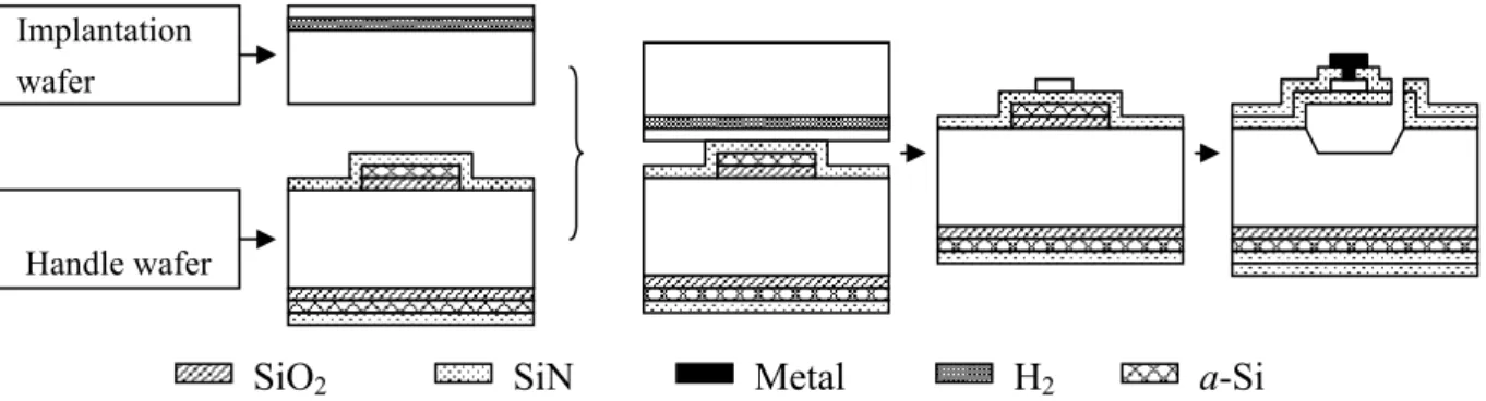
Single crystalline silicon was mainly used for the piezoresistive aero-acoustic microphone fabrication due to its high gauge factor [18, 23]. Bonding techniques were used, including the high temperature fusion bonding technique and plasma enhanced low temperature direct bonding technique. Figure 1.3 presents the simplified process flow of the fusion bonding technique. The handle wafer was firstly patterned to form the cavity shape and the SOI wafer was deposited with silicon nitride (SiN) material. Then, these two wafers were fusion bonded together and the top SOI wafer was etched back to the top silicon layer. Finally, this silicon layer was used as the piezoresistive sensing layer to fabricate the piezoresistors.
Figure 1.3: Process flow of the fusion bonding technique.
Figure 1.4 presents the simplified process flow of the low temperature direct bonding with smart-cut technique. The handle wafer was firstly patterned with sacrificial layers and covered with silicon nitride material. The implantation wafer was heavily doped with hydrogen. After plasma surface activation, these two wafers were bonded together at room temperature and annealed at 300℃ to increase the bonding strength. Then, a higher temperature annealing at 550℃ was carried out. The heavily doped hydrogen formed gas bubbles at this temperature, and this led to micro-cracks in the doping areas. Finally, a thin silicon layer was separated and transferred to the handle wafer. This transferred silicon layer was used as the piezoresistive sensing material, and finally, the diaphragm was released using the surface micromachining technique.
SiO2 SiN Metal
SOI wafer
Handle wafer
Figure 1.4: Process flow of the low temperature direct bonding with smart-cut technique.
Although the single crystalline silicon material has a large gauge factor, the bonding process complicates the process flow and the bonding technique does not offer a high yield. Later in this thesis, re-crystallized polycrystalline silicon material will be introduced to replace the single crystalline silicon material to fabricate the piezoresistors.
SiO2 SiN Metal H2 a-Si
Handle wafer Implantation wafer
1.4 Summary
The clear goal of this thesis is proposed in this chapter. The wide-band MEMS aero-acoustic microphone discussed in this thesis is defined to have a large bandwidth of several hundreds of kHz and dynamic range up to 4kPa. After comparison with other sensing mechanisms such as the piezoelectric and capacitive types, a piezoresistive sensing mechanism is chosen based on the SBW scaling properties.
1.5 References
[1] B. Baligand and J. Millet, "Acoustic Sensing for Area Protection," in Battlefield Acoustic Sensing for ISR Applications, pp. 4-1-4-12, 2006.
[2] S. Oerlemans, L. Broersma, and P. Sijtsma, "Quantification of airframe noise using microphone arrays in open and closed wind tunnels," National Aerospace Laboratory NLR, Report, 2007.
[3] M. Remillieux, "Aeroacoustic Study of a Model-Scale Landing Gear in a Semi-Anechoic Wind-Tunnel," MSc Thesis, Department of Mechanical Engineering, Virginia Polytechnic Institute and State University, 2007.
[4] A. Bale, "The Application of MEMS Microphone Arrays to Aeroacoustic Measurements, MASc Thesis, Department of Mechanical Engineering, University of Waterloo, 2011.
[5] S. A. McInerny and S. M. Olcmen, "High-intensity rocket noise: Nonlinear propagation, atmospheric absorption, and characterization," The Journal of the Acoustical Society of America, vol. 117, pp. 578-591, February 2005.
[6] P. R. Scheeper, B. Nordstrand, J. O. Gullv, L. Bin, T. Clausen, L. Midjord, and T.
Storgaard-Larsen, "A new measurement microphone based on MEMS technology,"
Microelectromechanical Systems, Journal of, vol. 12, pp. 880-891, 2003.
[7] S. Hansen, N. Irani, F. L. Degertekin, I. Ladabaum, and B. T. Khuri-Yakub, "Defect imaging by micromachined ultrasonic air transducers," in Ultrasonics Symposium Proceedings, pp. 1003-1006 vol.2, 1998.
[8] T. Lavergne, S. Durand, M. Bruneau, N. Joly, and D. Rodrigues, "Dynamic behavior of the circular membrane of an electrostatic microphone: Effect of holes in the backing electrode," The Journal of the Acoustical Society of America, vol. 128, pp. 3459-3477, 2010.
[9] V. Magori and H. Walker, "Ultrasonic Presence Sensors with Wide Range and High Local Resolution," Ultrasonics, Ferroelectrics and Frequency Control, IEEE Transactions on, vol. 34, pp. 202-211, 1987.
[10] P. R. Scheeper, A. G. H. D. v. der, W. Olthuis, and P. Bergveld, "A review of silicon microphones," Sensors and Actuators A: Physical, vol. 44, pp. 1-11, 1994.
[11] R. Schellin and G. Hess, "A silicon subminiature microphone based on piezoresistive polysilicon strain gauges," Sensors and Actuators A: Physical, vol. 32, pp. 555-559, 1992.
[12] M. Sheplak and J. Dugundji, "Large Deflections of Clamped Circular Plates Under Initial Tension and Transitions to Membrane Behavior," Journal of Applied Mechanics, vol. 65, pp. 107-115, March 1998.
[13] M. Rossi, "Chapter 5, 6," in Acoustics and Electroacoustics, Artech House, Inc., 1988.
[14] S. D. Senturia, "Chapter 1, 17," in Microsystem Design, Kluwer Academic Publishers, 2001.
[15] D. Martin, "Design, fabrication, and characterization of a MEMS dual-backplate capacitive microphone," Ph.D Thesis, Deparment of Electrical and Computer Engineering, University of Florida, 2007.
[16] S. T. Hansen, A. S. Ergun, W. Liou, B. A. Auld, and B. T. Khuri-Yakub, "Wideband micromachined capacitive microphones with radio frequency detection," The Journal of the Acoustical Society of America, vol. 116, pp. 828-842, August 2004.
[17] D. P. Arnold, S. Gururaj, S. Bhardwaj, T. Nishida, and M. Sheplak, "A piezoresistive microphone for aeroacoustic measurements," in Proceedings of International Mechanical Engineering Congress and Exposition, pp. 281-288, 2001.
[18] M. Sheplak, K. S. Breuer, and Schmidt, "A wafer-bonded, silicon-nitride membrane microphone with dielectrically-isolated, single-crystal silicon piezoresistors," in Technical Digest. Solid-State Sensor and Actuator Workshop . Transducer Res, Cleveland, OH, USA, pp. 23-26, 1998.
[19] S. Horowitz, T. Nishida, L. Cattafesta, and M. Sheplak, "A micromachined piezoelectric microphone for aeroacoustics applications," in Proceedings of Solid-State Sensor and Actuator Workshop, 2006.
[20] M. D. Williams, B. A. Griffin, T. N. Reagan, J. R. Underbrink, and M. Sheplak, "An AlN MEMS Piezoelectric Microphone for Aeroacoustic Applications,"
Microelectromechanical Systems, Journal of, vol. 21, pp. 270-283, 2012.
[21] J. Hillenbrand and G. M. Sessler, "High-sensitivity piezoelectric microphones based on stacked cellular polymer films (L)," The Journal of the Acoustical Society of America, vol.
116, pp. 3267-3270, 2004.
[22] K. Kadirvel, R. Taylor, S. Horowitz, L. Hunt, M. Sheplak, and T. Nishida, "Design and Characterization of MEMS Optical Microphone for Aeroacoustic Measurement," in 42nd Aerospace Sciences Meeting & Exhibit, Reno, NV, 2004.
[23] Z. J. Zhou, L. Rufer, and M. Wong, "Aero-acoustic microphone with layer-transferred single-crystal silicon piezoresistors," in Solid-State Sensors, Actuators and Microsystems Conference, TRANSDUCERS 2009. International, pp. 1916-1919, 2009.
Chapter 2: MEMS Sensor Design and Finite Element Analysis
For MEMS sensor design, basic material properties, such as Young’s modulus, density and residual stress, are important. The density decides the total mass of the sensing diaphragm, and Young’s modulus and residual stress decide the effective spring constant of the sensing diaphragm. The total mass and the effective spring constant then fix the first mode resonant frequency of the sensor. In this chapter, first, techniques and methods to accurately measure these material properties are introduced. Then, design considerations based on different fabrication techniques are described, and finally, the design parameters are presented and each design is simulated using the finite element analysis (FEA) method.
2.1 Key Material Properties
2.1.1 Diaphragm Material Residual Stress
After the thin film deposition process, normally, the film will contain residual stress, which is mostly caused either by the difference of the thermal expansion coefficient between the thin film and the substrate or by the material property differences within the interface between the thin film and the substrate, such as the lattice mismatch. The first of these is called thermal stress and the latter is called intrinsic stress.
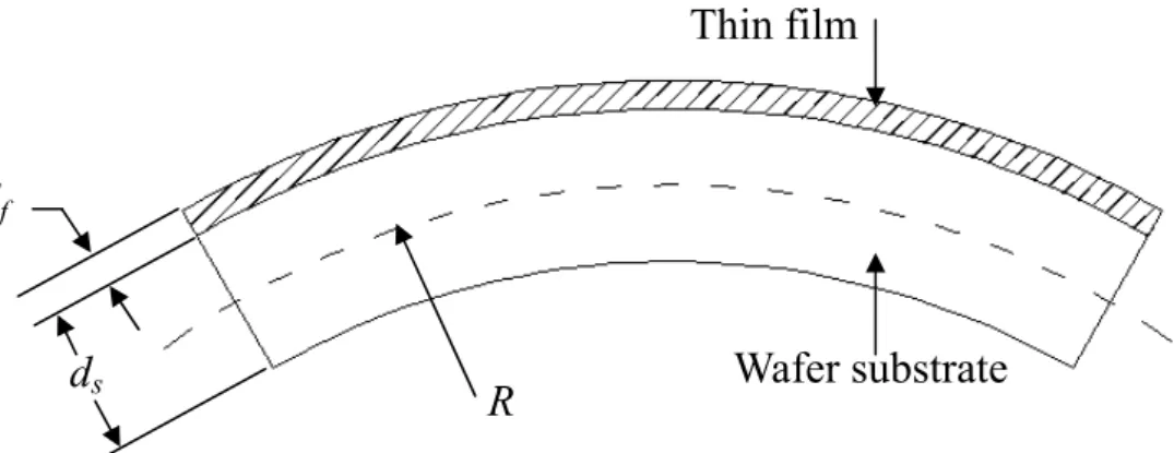
In 1909, Stoney [1] found that after deposition of a thin metal film on the substrate, the film-substrate system would be bent due to the residual stress of the deposited film (Figure 2.1). Then he gave the well-known formula in Equation 2.1 to calculate the thin film stress based on the measurement of the bending curvature of the substrate, where σ is the thin film residual stress, Es is the substrate material Young’s modulus, ds is the substrate thickness, df is the thin film thickness, νs is the substrate material Poisson’s ratio and R is the bending
curvature.
Figure 2.1: Bending of the film-substrate system due to the residual stress.
f s s s
d R
d E
) 1 ( 6
2
(2.1)
For the stress measurement experiment, before the thin film deposition process, the initial curvatures of two P-type (100) bare silicon wafers are measured as Ri. As will be described in Chapter three, the sensing diaphragm material used in the fabrication process is low-stress silicon nitride (LS-SiN) film. So, on one wafer, a 0.5μm thick LS-SiN film is deposited, and on the other wafer, a 1μm thick film is deposited. The backside nitride materials on both wafers are etched away though a reactive ion etching (RIE) process. Then the bending curvature of the wafer after thin film deposition is measured as Rd. The curvature R in Equation 2.1 is calculated by R = Rd – Ri. Table 2.1 presents the value used in Equation 2.1 for calculation and the result of the calculated residual stress.
Table 2.1: Curvature method measurement parameters and results.
Es (GPa) νs ds (μm) df (μm) R (m) σ (MPa)
185 0.28 525 0.5 143.1 165 185 0.28 525 1 55.2 214
Stoney formula is based on the assumption that df << ds, and the calculated result is an average value of the stress within the whole wafer. Rotational beam method [2] is another
ds Wafer substrate
Thin film
R df
commonly used technique to measure the thin film residual stress, and the advantage of this method is that the stress value can be measured locally. Figure 2.2 presents the layout of a single die of the microphone chip. At the center of the die, two rotational beam structures (marked within the black dashed line) are placed perpendicularly to measure the residual stress in both the x and y directions.
Figure 2.2: Layout of a single die.
The details of the rotational beam structures are shown in Figure 2.3. With the design parameters listed in Table 2.2, the residual stress calculation equation is
) 6490E (MPa
, (2.2)
where E is the beam material Young’s modulus and δ is the beam rotation distance under
stress. The drawback of this method is obviously that unless we know the beam material Young’s modulus very well, the calculated residual stress value is not accurate. In section 2.1.2, the method to measure the material Young’s modulus will be introduced and here we will directly use the measured value 207 GPa to calculate the residual stress. Figure 2.4(a and b) presents two typical results of two structures rotated after releasing. The rotation distances are 5.5 and 4μm and the corresponding residual stresses are 175MPa and 128MPa for 1μm and 0.5μm thick LS-SiN material, respectively. The residual stress values measured by rotational beam method are about 20% less than the values measured by the curvature method.
This phenomenon is also observed by Mueller et al. [3], and the reason for it is the stiction between the indicating beam of the rotating structure and the substrate, which causes the beams to not be in their equilibrium state when they are stuck down.
Figure 2.3: Layout of the rotational beam structure.
Table 2.2: Rotational beam design parameters.
Wr (μm): 30 Wf (μm): 30
Lf (μm): 300 Lr (μm): 200
a (μm): 4 b (μm): 7.5 h (μm): 10
Wr
Wf
Lf
a b
h
Lr
(a): Rotational beam (film thickness 1.1μm) (b): Rotational beam (film thickness 0.5μm) Figure 2.4: Microphotography of two typical rotational beams after releasing.
2.1.2 Diaphragm Material Density and Young’s Modulus
Diaphragm material density and Young’s modulus are important for mechanical vibration performance estimation. The density will determine the total mass of the diaphragm and the Young’s modulus will determine the spring constant. Both of these two values are indirect calculation results from the measurement of first mode resonant frequencies of doubly-clamped beam structures with different lengths.
Equation 2.3 is used to calculate the first mode resonant frequency of a doubly-clamped beam structure based on the Rayleigh–Ritz method, where ω is the resonant frequency in the unit of rad/s; t and L are the thickness and length of the beam; and E, ρ and σ are the Young’s modulus, density and residual stress of the beam material, respectively [4]. As we already know the residual stress from using the methods described in the previous section, especially the average value from the curvature method, by measuring the first mode resonant frequencies ω1 and ω2 of two doubly-clamped beams with same cross-sectional area but different lengths L1 and L2, the Young’s modulus and density of the beam material can be expressed by Equations 2.4 and 2.5. Figure 2.5 presents the layout of different doubly-clamped beams (also marked within the red dashed line in Figure 2.2) and Table 2.3 presents the dimension of these beams.
2 442 22 3 2 9
4
L L
E t
(2.3)
30μm
30μm
4 2 2 1 2 2 4 1
2 1 2 2 2 1 2 2
2 1 1
1 1 2 3
L L
L L E t
(2.4)
2 1 4 1 2 2 4 2
2 1 2 2 2
3 2
L L
L L
(2.5)
Figure 2.5: Layout of the doubly-clamped beams.
Table 2.3: Dimension of different beams (length×width [μm×μm]).
1 2 3
A 200×10 150×10 100×10
B 200×20 150×20 100×20
C 200×30 150×30 100×30
D 200×40 150×40 100×40
E 200×50 150×50 100×50
The resonant frequency of the doubly-clamped beam is measured by a Fogale Laser vibrometer, and the setup is shown in Figure 2.6. The sample die is stuck to a piezoelectric plate with silicone (RHODORSIL™), and the piezoelectric plate is glued to a small printed circuit board (PCB) with silver conducting glue. This prepared sample is fixed to a vibration free stage using a vacuum. During the measurement, a sinusoid signal is connected to the
piezoelectric plate and the input frequency is swept within a large bandwidth from 10kHz up to 2MHz. The laser point of the vibrometer is focused at the center of the beam and the corresponding vibration displacement amplitude is recorded. A typical recorded signal is shown in Figure 2.7. The red line is the signal measured at the center of the beam and the blue line is the signal measured at the fixed point on the substrate near the beam. All measured data are shown in Table 2.4.
Figure 2.6: Resonant frequency measurement setup.
Figure 2.7: Typical measurement result of the laser vibrometer.
Vibration free stage
Piezoelectric disk Laser (Fogale vibrometer )
PCB
Sample die
PCB
Piezoelectric plate Sample die
Table 2.4: First mode resonant frequencies of different beams (1μm thick).
1 2 3
A 607.0kHz 855.6kHz 1.511MHz
B 601.8kHz 844.4kHz 1.476MHz
C 597.6kHz 835.6kHz 1.450MHz
D 594.0kHz 833.4kHz 1.459MHz
E 596.0kHz 832.4kHz 1.449MHz
Substituting the variables in Equation 2.4 and 2.5 by using the data in Table 2.3 and Table 2.4, the calculated average density and Young’s modulus of the deposited LS-SiN material are 3002kg/m3 and 207GPa, respectively.
2.2 Design Considerations
To design a wide-band high frequency microphone, not only should the device performance specifications mentioned in Chapter one (considering the mechanical and acoustic performances) and the material properties mentioned in this chapter be considered, but also the device fabrication process’s feasibility. The design of the physical structure should also accompany the design of the fabrication process.
To achieve a suspending diaphragm on top of an air cavity, generally, there exist two methods.
One is to use the surface micromachining technique in which the thin film sacrificial layers are used (Figure 2.8). The diaphragm material is deposited on top of the sacrificial layers, and finally, by etching away the sacrificial layers, the diaphragm is released and suspended in the air. Another method is based on the bulk micromachining technique in which the backside silicon substrate etching is involved (Figure 2.9). Depending on whether the dry etching method or wet etching method is used, the sidewall of the backside cavity will be perpendicular to the diaphragm surface or be on an angle to the diaphragm surface.
Figure 2.8: Surface micromachining technique.
Silicon substrate Sacrificial layer(s) Diaphragm layers
Figure 2.9: Bulk micromachining technique.
The surface micromachining and bulk micromachining techniques have their different achievable aspects and limitations for the microphone design. Figure 2.10 demonstrates a cross-section view of the physical structure of the wide-band high frequency microphone device that will be fabricated by using the surface micromachining technique. The achievable aspects are the following: (1) The dimension of the suspended sensing diaphragm could be independent with the air gap thickness below itself (the diaphragm dimension is controlled to achieve the required resonant frequency and acoustic sensitivity, and the air gap thickness is chosen to modulate the squeeze film damping effect to achieve a flat frequency response within the interested frequency bandwidth). (2) The reverse pyramidal dimple structure (the effective contact area between the diaphragm and the cavity surface is shrunk) is introduced into the sensing diaphragm to prevent the common stiction problem in the surface
Silicon substrate Hard mask layer Diaphragm layers
micromachining fabrication process. The limitations of this technique are the following: (1) Release holes/slots will be opened on the sensing diaphragm, which leads to an acoustic short path between the ambient space and the cavity underneath the diaphragm. This acoustic short path will limit the low frequency performance of the microphone because at low frequency, any change in the pressure of the ambient space (upper-side of the sensing diaphragm) will propagate quickly into the cavity under the sensing diaphragm through the release holes/slots.
Then the pressure difference is equalized. (2) Due to the possible attacking of the front-side metallization by the etching solutions, the process compatibility should be well designed. We have two choices to achieve this fabrication process: one is to form the cavity first and then do the metallization, and the other is to do the metallization first and form the cavity last. The first method would not need the consideration of the compatibility of the etching solution and the metallization system. But after forming the cavity, either photolithography or the wafer dicing would be very difficult since both of them would affect the device yield dramatically.
Using the second method, the device could be released at the final stage, even after the wafer dicing, but the key point would be to find a way either to protect the metallization during the etching or make the metallization itself resistant to the etching solutions.
Figure 2.11 demonstrates a cross-section view of the physical structure of the wide-band high frequency microphone device that will be fabricated using the bulk micromachining technique.
The achievable aspects are the following: (1) It is a relatively simple process, and there are less compatibility issues between the front-side metallization and the releasing chemicals. (2) Because there is a full diaphragm without holes/slots, which prevents the acoustic short path effect, the low frequency property of the microphone will be improved. The limitations of this technique are the following: (1) Due to the backside etching characteristic, the air cavity under the sensing diaphragm will be very large (air cavity thickness equal to the substrate thickness). In this situation, the squeeze film damping effect of the air cavity can be ignored and this means that the sensing diaphragm will not be damped. A high resonant peak will exist in the microphone frequency response spectrum.