HAL Id: tel-00012070
https://tel.archives-ouvertes.fr/tel-00012070
Submitted on 31 Mar 2006
HAL is a multi-disciplinary open access archive for the deposit and dissemination of sci- entific research documents, whether they are pub-
L’archive ouverte pluridisciplinaire HAL, est destinée au dépôt et à la diffusion de documents scientifiques de niveau recherche, publiés ou non,
GaN et InGaN dopées avec des ions terres rares
Thomas Andreev
To cite this version:
Thomas Andreev. Propriétés optiques et structurales de boîtes quantiques GaN et InGaN dopées avec des ions terres rares. Physique [physics]. Université Joseph-Fourier - Grenoble I, 2006. Français.
�tel-00012070�
Université Joseph Fourier – Grenoble I Sciences & Géographie
THÈSE
Pour obtenir le grade de
DOCTEUR DE L’UNIVERSITÉ JOSEPH FOURIER
Physique
Présentée et soutenue publiquement par
Thomas Andreev
le 29 mars 2006
Growth and Optical Properties of GaN and InGaN Quantum Dots doped with Rare Earth ions
Composition du jury :
Benoît BOULANGER Président
Daniel LE SI DANG Examinateur
Pierre LEFÈBVRE Rapporteur
Georges BOULON Rapporteur
Bruno DAUDIN Directeur de thèse
Cette thèse a été préparée au sein du CEA Grenoble Département de Recherche Fondamentale sur la Matière Condensée
Service de Physique des Matériaux et des Microstructures
Offen auf alles Neue zuzugehen, ohne das Detail aus dem Auge zu verlieren, erlaubt so manche unerwartete Entdeckung.
Remerciement
Pour commencer je voudrais remercier Prof. Pierre Lefèbvre et Prof. Georges Boulon d’avoir accepté de rapporter ce travail avec intérêt.
Ce travail a été effectué au sein de l’équipe mixte CEA-CNRS-UJF
« Nano-physique et semi-conducteurs « du Sevice de Physique des Matériaux et Microstructures (DRFMC/ SP2M). A ce titre, je remercie Jean Michel Gérard et Noël Magnéa de m’avoir accueilli dans ce laboratoire.
Je voudrais remercier chaleureusement toutes les personnes qui m’ont aidé pendant ces trois ans de thèse.
Je remercie Bruno Daudin, mon directeur de thèse, pour la confiance qu’il m’a témoigne. Il m’a laissé une grande liberté pour donner des accents personnels à mon travail de thèse. En plus de cette liberté, il a toujours su être une oreille ouverte pour me donner des conseils et m’encourager. Il m’a aussi donné la possibilité d’apprendre plusieurs techniques expérimentales.
Un grand merci à Mitsuhiro Tanaka et Osamu Oda qui ont toujours témoigné beaucoup d’intérêt pour mon travail, ainsi qu’à tous les employés de l’entreprise NGK INSULATORS. Cette entreprise a généreusement financé beaucoup d’équipement pour le laboratoire comme la machine MBE et aussi mon travail de thèse.
Un merci particulier à mon collaborateur Yuji Hori de l’entreprise NGK INSULATORS. En début de thèse il m’a enseigné la méthode
MBE et m’a très bien introduit dans le projet. Je voudrais aussi le remercier pour la croissance de nombreux échantillons de très bonne qualité, que j’ai pu étudier en optique.
L’entreprise DOWA MINING est remerciée pour la participation au financement d’une partie de mon travail de dernière année.
Personnellement je voudrais remercier Hiroyuki Togawa, Hideaki Kobayashi et Akira Otsuka pour les discussions qu’elles soient du domaine de la physique ou non.
Un grand merci aussi à Eva Monroy, Bruno Gayral et Frederic Fossard pour les nombreuses discussions physiques et non physiques.
Au début de ma thèse ils m’ont donné beaucoup de conseils en optique, et par la suite, sur l’organisation du manuscrit et des publications toujours de façon très gentille.
Pendant ma thèse, j’ai eu la chance de travailler avec Daniel Le Si Dang, professeur, spécialiste de la caractérisation optique. Il m’a toujours encouragé et dispensé de très bons conseils, et ce, à chaque fois de façon très cordiale. Merci aussi pour les nombreuses discussions physique et non physique que j’ai pu avoir avec lui.
C’est avec plaisir que je voudrais remercier Nguyen Quang Liem, professeur de Vietnamese Academy of Science and Technology, pour le formidable travail qui a découlé de notre collaboration sur les caractérisations optiques. Nguyen Quang Liem m’a beaucoup appris,
beaucoup des idées qui sont elles aussi responsables sur le succès de ce travail.
Un grand merci aussi à Denis Jalabert pour se explications sur la caractérisation structurelle par RBS, toujours avec humour et décontraction.
Xavier Biquard est remercié pour avoir très bien diriger l’expérience d’EXAFS à l’ESRF. Il est aussi remercié pour plusieurs analyses et discussions.
Je voudrais remercier aussi les étudiants du laboratoire du CEA pour la création d’une ambiance très sympathique. Le travail avec vous a été très agréable, ainsi que tous les week-ends que nous avons pu faire ensemble en montagne. De plus, un grand merci à tout les amis que j’ai rencontré à Grenoble et qui m’ont permis de passer des moments légers, amusants et intéressants ici en France.
Un gentil merci à Marlène Terrier, Yann Genuist, Gilbert Demoment et Yoann Curé, le personnel technique de laboratoire pour la rapidité de leurs réactions face aux divers problèmes posés pendant cette thèse.
Je voudrais remercier Fabrice Donatini pour l’installation de la Cathodoluminescence et pour sa pédagogie lors de ses explications.
Un très grand merci aussi à Virgine Charmard, qui m’a aidé à bien m’installer en France et pour les encouragements qu’elle m’a donnés.
Merci à Metin Tolan et Heinz Hövel, professeurs de l’Université de Dortmund pour leur intérêt porté à mon travail et pour plusieurs présentations invitées.
Je voudrais remercier aussi tous mes amis Allemands et non Allemands et mes parents, qui m’ont eux aussi très bien encouragé pendant les trois ans de thèse.
Résumé
Ce travail présente des résultats sur les propriétés optiques et structurales de boîtes quantiques III-nitrures dopées terres rares.
L’idée sous-jacente de ce travail est la fabrication d’une diode blanche à base de boîtes quantiques dopées terres rares en mélangeant les couleurs – Eu(rouge), Tm(bleu) et Tb(vert) – de leurs luminescences.
Deux choses importantes ont été étudiées. La première question porte sur la façon dont les terres rares modifient le régime de croissance lors de l’épitaxie par jets moléculaires et sur la localisation des atomes de terres rares dans les structures.
Le deuxième, quant à elle, a pour sujet les propriétés optiques des terres rares dans des boîtes (In)GaN. Il est important de comparer les propriétés optiques des terres rares dans les boîtes avec les propriétés d’une couche afin de comparer l’efficacité quantique de ces deux systèmes. A cette étude s’ajoute le problème du transfert d’énergie du matériau semi-conducteur vers les ions terre rare.
Croissance de structures à boîtes dopées terres rares à base de nitrures
Le premier chapitre répond à la première question : l’influence des terres rares durant la croissance et leur position dans les structures de boîtes GaN dopées terres rares dans l’AlN. Cette étude a principalement nécessité l’utilisation de méthodes structurales comme l’AFM, le RHEED, l’EXAFS et le RBS.
Pendant la croissance MBE, les atomes de terres rares ont tendance à ségréger à la surface. Cet effet est extrêmement visible dans le cas de l’Eu pour lequel la morphologie des boîtes GaN est drastiquement modifiée en fonction des concentrations. Au contraire, les boîtes GaN dopées Tm ne sont pas beaucoup affectées par la présence de Tm, ce qui prouve que le régime de croissance est totalement différent.
Il est aussi possible de réaliser des boîtes GaN dopées Tm avec des concentrations de l’ordre de 10%, contrairement aux boîtes Eu, pour lequel un dopage de plus de 3% supprime la formation des boîtes, ainsi que le révèle l’AFM.
Cette influence totalement différente du Tm et de l’Eu dans la formation des boîtes peut être expliquée par différentes localisations des terres rares dans les structures de boîtes GaN encapsulées dans l’AlN. Les résultats d’EXAFS et de RBS montrent que l’Eu est bien incorporé dans les boîtes alors que le Tm se trouve à l’interface des boîtes GaN/AlN et plutôt dans l’AlN.
Propriétés optiques d’une couche GaN dopée Eu
Ce chapitre développe une étude optique sur une couche GaN dopée Eu. Plusieurs nouvelles transitions intra 4f d’Eu partant des niveaux 5D2, 5D1 et 5D0 ont été identifiées et montrent différentes
intense des transitions d’Eu dans le rouge, a des raies bien séparées.
Les différentes caractéristiques comme la structure fine des raies, la dépendance en température, la profondeur de pénétration des électrons par cathodoluminescence et la photoluminescence en fonction de la puissance, montrent qu’il y a deux types de sites différents : le premier proche de la surface, le deuxième à l’intérieur des échantillons.
Les transferts d’énergie, dont l’étude est basée sur des mesures par excitation de photoluminescence (PLE), nous montrent que les ions d’Eu sont excités par un mécanisme à l’energie du gap de GaN.
L’excitation par les défauts est plus de cent fois plus faible que celle due au gap du GaN, elle n’a aussi été détectée que pour les ions à l’intérieur des échantillons. Les transitions fines (0.2 nm) permettent d’observer un décalage vers le bleu ce qui est dans la direction opposée aux décalages typiques des gaps avec la température croissante.
Propriétés optiques de boîtes quantiques GaN dopées avec Eu
Ce chapitre développe une étude optique sur les boîtes GaN dopées Eu. L’influence de la concentration d’Eu sur un spectre de photoluminescence est aussi discutée. Sur ce spectre, on peut observer une signature des boîtes à 300 nm ainsi que des raies fines à 622 nm. A faible concentration d’Eu, la signature des boîtes est plus prononcée et les raies d’Eu ont une intensité faible. En augmentant la
quantité d’Eu, la signature des boîtes baisse d’intensité et les émissions d’Eu dominent le spectre. Ce résultat montre qu’il existe un transfert énergétique entre les porteurs situés dans les boîtes quantiques et les ions d’Eu. Il est montré que le nombre d’atomes Eu mesuré par RBS est proportionnel à l’intensité de la luminescence. A partir de ce constat, un modèle simple permet de calculer le temps de vie radiatif des ions Eu.
La photoluminescence en fonction de la température des ions Eu dans les boîtes GaN est stable de la température de l’hélium liquide à l’ambiante. A l’opposé, une couche de GaN dopée Eu et des boîtes non dopées perdent 90% de leur luminescence ce qui montre la grande efficacité quantique des structures à boîtes dopées Eu. Le mécanisme déterminant est la localisation des porteurs dans les boîtes (sans défauts) parallèlement au piégeage rapide des porteurs par les terres rares.
L’émission d’Eu double entre 5 K et la température ambiante pour un échantillon à basse concentration d’Eu (0.4%). Cette dépendance de la photoluminescence de l’Eu avec les faibles concentrations d’Eu est difficile à interpréter.
Nous avons trouvé que la durée de vie d’Eu est plus longue dans les boîtes quantiques GaN que dans une couche GaN dopée Eu.
Ceci pose la question de la localisation microscopique de l’Eu dans
Les ions excités de cette façon ont typiquement des durées de vie plus longues.
Il est montré que l’influence de la taille des boîtes sur la luminescence d’Eu est négligeable.
Boîtes InGaN dopées Eu
Les structures à base de boîtes quantiques InGaN dopées terres rares sont intéressantes pour l’injection de courant, car il est possible, contrairement à l’AlN, de contrôler le dopage p- et n- du GaN.
Dans ce chapitre nous avons discuté les propriétés optiques des boîtes InGaN dopées Eu. La question de la localisation d’Eu dans des structures de boîtes InGaN encapsulées dans le GaN est abordée. Une étude de l’excitation de photoluminescences (PLE) montre que l’Eu peut être trouvé dans les boîtes et aussi dans la barrière de GaN. Ceci peut être expliqué par la forte ségrégation de l’Eu lors de la croissance des boîtes.
La signature de l’Eu dans la barrière montre une diminution de l’intensité de la photoluminescence en fonction de la température (de 5 K à 300 K). Par contre, les raies d’Eu dans les boîtes InGaN restent stables, ceci peut être comparé au comportement de l’Eu dans les boîtes GaN.
Boîtes GaN dopées Tm
Les boîtes quantiques dopées Tm sont intéressantes pour l’émission dans le bleu.
Dans un premier temps, ce chapitre traite de la position des terres rares dans des structures à boîtes GaN dopée Tm encapsulées dans l’AlN. En photoluminescence, seules les boites sont excitées, des raies larges dans le bleu sont visibles. En cathodoluminescence, toute la structure est excitée et les raies de Tm dans les boîtes sont encore visibles et on note, de plus, avec un décalage de 2 nm, la signature du Tm dans la barrière d’AlN. Ce résultat montre que les boîtes sont réellement dopées avec Tm mais que celui-ci peut être également trouvé dans la barrière d’AlN.
Aucune dépendance en température (5 K - 300 K) de la photo- luminescence n’est observée pour les transitions à partir du niveau
1D2, ce qui est important pour l’émission dans le bleu. Dans le même temps, les transitions du niveau 1I6 perdent deux ordres de grandeur dans leur photoluminescence. Les émissions des transitions des états excités 1G4 et 3H4 ont une dépendance intermédiaire et diminuent d’un ordre de grandeur. Ces différents comportements thermiques permettent d’identifier de nouvelles raies et de construire un diagramme d’énergies.
L’excitation de photoluminescences (PLE) montre que les ions de Tm sont excités par un transfert d’énergie provenant des boîtes.
Pour préciser le mécanisme d’excitation du Tm, des mesures de temps de vie ont été analysées. Il est observé que le temps de vie du
de température. On peut ainsi conclure qu’il existe un deuxième canal de transfert d’énergie d’excitation dans le niveau 1D2. Ce canal est actif pour des températures élevées probablement depuis les niveaux
1I6, par un mécanisme de relaxation ou de transfert retour depuis un niveau de piège, et excite ensuite la terre rare.
Nous avons observé que les temps de vie des transitions du niveau 1I6 sont en général plus courts que les transitions du 1D2 ceci étant en concordance avec la littérature.
Une étude a été effectuée sur des structures AlGaN dopées Tm.
Elle montre des raies similaires aux boîtes GaN dopées Tm dans le bleu. Un effet de clusterisation doit probablement se produire pendant la croissance, ainsi l’environnement des atomes d’Eu consiste en des atomes de Ga (pas d’Al) et la structure a des similarités avec des boîtes.
Propriétés optiques des boîtes GaN dopées Tb
Nous nous sommes intéressé dans cette partie à la position des terres rares dans les structures à boîtes GaN dopées Tb encapsulées dans l’AlN. Les boîtes dopées Tb montrent une forte luminescence dans le vert.
Une étude optique de la photoluminescence en fonction de la température de structures à boîte GaN dopée Tb et d’un échantillon de référence d’AlN dopé Tb nous a permis de mettre en évidence le dopage au Tb dans les boîtes et dans l’AlN. Le comportement en
température de la photoluminescence des boîtes GaN dopées Tb permet d’identifier plusieurs transitions.
Une couche de GaN dopée Tb a une luminescence de très faible intensité. Ceci est reporté dans la littérature et est expliqué par les symétries des ions Tb dans le GaN.
Luminescence blanche des boîtes GaN dopées terres rares
Des structures à boîtes quantiques de GaN dopées avec des concentrations ajustées de Eu(rouge), Tm(bleue) et Tb(vert) ont montré de la luminescence blanche, ceci est particulièrement intéressant pour des applications dans l’éclairage. La couleur et l’intensité sont stables de l’ambiante jusqu'à des températures élevés, de l’ordre de 450 K.
La première étape d’injection de porteurs est réalisée par un contact Schottky pour les boîtes GaN dopées Eu (rouge). La couleur trouvée est plus jaune en électroluminescence qu’en photoluminescence, ceci montre qu’il existe différents mécanismes d’excitation des terres rares.
Content
1. Introduction 1
2. Kinetics of rare earth luminescence in semiconductors 7
2.1 Rare earth related trap levels in semiconductors……….. 7
2.2 Energy transfer mechanism from the semiconductor host to the RE3+ ions…...… 8
3. Growth of undoped and rare earth doped nitride homo- and heterostructures 13 3.1 Growth of GaN and AlN layers………. 13
3.2 The Stranski Krastanow growth mode……… 15
3.2.1 Growth of GaN QDs on AlN……….. 16
3.2.2 Growth of GaN QDs on AlGaN……… 17
3.3 Rare earth doped GaN and AlN layers………... 19
3.3.1 Growth of GaN:Eu layers……….. 21
3.3.2 Remarks on the growth of Eu doped AlN………... 21
3.3.3 Rare earth incorporation in GaN versus AlN for the example of Tm………. 22
3.3.4 Growth of Tb doped GaN layers……….. 23
3.4 Rare earth doped GaN quantum dots………. 24
3.4.1 Growth of GaN QDs doped with Eu……… 24
3.4.2 EXAFS on GaN QDs doped with Eu………... 26
3.4.3 Growth of GaN QDs doped with Tm……… 28
3.4.4 Tm location in the GaN QDs grown in an AlN matrix………... 30
3.4.5 Growth of GaN QDs doped with Tb and the influence of the substrate temperature………. 31 3.4.6 Closing remarks to growth of GaN:RE QDs on AlN………. 33
3.5 Growth and morphological properties of InGaN:Eu QDs………. 35
4. Optical properties of GaN:Eu layers 41 4.1 The emission spectrum of GaN:Eu layers……….. 41
4.2 Eu sites in GaN:Eu layers and their excitation mechanism………. 46
5. Optical properties of GaN QDs doped with Eu 57 5.1 The influence of the Eu concentration on the emission spectrum……….. 57
5.2 Temperature dependent PL of GaN:Eu QDs………. 60
5.2.1 Temperature dependent PL of GaN:Eu QDs with different contents………. 62
5.3 Time resolved PL of GaN:Eu QDs……….. 63
5.4 The effect of the GaN QDs size onto the Eu emission………. 65
6. Optical properties of InGaN QDs doped with Eu 69 6.1 Eu location in InGaN QDs sandwiched in GaN spacing layers……….. 69
6.2 Temperature dependence of the Eu3+ PL of InGaN:Eu QDs………. 75
6.3 Applicability of InGaN:RE QDs for full color devices……… 77
7. Optical properties of GaN:Tm QDs 79 7.1 Tm3+ location within the GaN:Tm QDs/AlN structure……… 79
7.2 Temperature dependent PL of GaN:Tm QDs……… 83
7.3 Excitation mechanism in Tm doped GaN QDs……….. 86
7.4 Optical properties of AlGaN doped with Tm……….. 93
8. Optical properties of GaN QDs doped with Tb 99 8.1 Optical properties of GaN:Tb layers……… 99
8.2 Optical properties in GaN:Tb QDs grown on AlN……….. 100
9. White luminescence from rare earth doped GaN QDs 107 9.1 Current injection via a metal semiconductor contact……… 110
10. Conclusion 113 11. Appendix A 115 11.1 Molecular beam epitaxy……… 115
11.2 Growth with in-situ RHEED……….. 117
11.3 Rutherford backscattering spectroscopy……… 118
11.4 Atomic force microscopy………... 121
11.5 Optical characterization methods……… 123
11.5.1 Photoluminescence……… 123
11.5.2 Photoluminescence excitation spectroscopy………. 126
11.5.3 Time resolved photoluminescence……….. 127
11.5.4 Cathodoluminescence………... 129
12. Appendix B 135
Publications 137
Rare earth (RE) ions with 3+ charge state have partly filled 4fn-shells, shielded from full filled outer orbitals (5s2 and 5p6). By contrast, RE ions with other charge states like RE2+ ions exhibit partly filled outer shells. This difference in the electronic structure has consequences on the optical properties of RE3+ and RE2+ ions in host materials. Emission from RE2+ ions is found to be broad due to a strong influence from the environment [Owe81, Par03] while emission from RE3+ ions is typically very sharp as a result of shielding from outer shells. These sharp emissions are extending from the ultraviolet (UV) up to the infrared (IR) spectral region, depending on the RE atom and of course the inner shell transition itself. The energy levels of the RE3+ ions have been extensively investigated in the 1960es and tabulated by Dieke and co- workers [Die68]. In the so called Dieke diagram (Appendix B) ground state and excited states from free RE3+ are listed so that the emission wavelength from each transition can be deduced. As the host material influence on the transition is typically weak, the Dieke diagram can be used to predict which emission can be expected from each rare earth ion.
Nevertheless, all inner RE3+ transitions are intrinsically forbidden. Only interactions, for example with other atoms (free REs) or symmetry breaking by the host material, can make them “less” forbidden. The consequences are long decay times, typically between 1 µs to 10 ms. In spite of these long decay times the advantage of the sharp and clear defined inner RE3+ transitions resulted in numerous applications. RE3+ ions are used as a phosphor for color lamps and displays [Lum05], in optical fiber telecommunication (Er and Pr) and last but not least in Laser applications like the Nd:YAG Laser or Nd:glass Laser.
The idea of combining the RE luminescence with a semiconductor host came out by using Er and Yb (infrared) in GaAs, GaP, Si and SiC. Especially Er doped Si structures have been well investigated since the research was driven by the appeal of integration with Si microelectronics. In Ref. [Fav89] a systematic reduction of thermal quenching of infrared Er luminescence has been found by increasing the band width of the host semiconductor.
2.0 3.0 4.0 5.0 6.0 7.0 0.0
1.0 2.0 3.0 4.0 5.0 6.0 7.0
SiC
Direct bandgap Indirect bandbap
Wavelenght (nm)
5000 1000 500 400 300
Ge GaP
InSb InAs
InP GaAs
CdTe CdSe ZnO ZnS
InN BN
GaN
Energy gap (eV)
Lattice constant (Å)
AlN
GaSb Diamond
Si
200
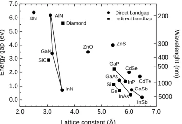
Figure 1.1: Band-gap and lattice constants of common semiconductors. Data from www.ioffe.rssi.ru.
For intense and thermally stable visible light emission from electroluminescence devices, wide band-gap semiconductors are required since efficient energy transfers can only occur if the band-gap of the host is wider than the energy difference between RE3+ ground states and excited state (Figure 1.1). Based on this idea, Steckl and his co-workers combined the RE3+ luminescent with the wide band-gap of GaN and realised electroluminescence from the blue to the red spectral range [Ste99, Hei99]. Furthermore the combination of different colors from RE3+ ions – red (Eu, Pr), green (Tb, Er, Ho) and blue (Tm, Dy, Ce) – would yield to white light emission. This idea is not new, as the combination of well defined RE-colors is used for example in mercury lamps where LaPO4:RE is used as a phosphor to obtain white light.
The choice of GaN as a semiconductor host can be further explained since it exhibits first a direct band-gap, required for a good semiconductor host - RE3+ ion energy transfer probability and since it is a III-V semiconductor so that RE ions are supposed to occupy metal sites with 3+ charge, which was later experimentally established [Ban02, Hor04].
However, the RE radiative quantum efficiency strongly depends on the carrier- mediated energy transfer process, which has to compete with fast non-radiative recombination channels. Non-radiative processes can occur for example at defects, which are found with a density of about 1010 /cm2 for GaN, which is a rather high number compared to other semiconductors. The result is a thermal quenching of the
improve significantly since QDs are defect free regions and act as carrier confinement centers so that the thermal stability of the observed RE luminescence should be enhanced drastically. In other words the energy transfer to RE ions will be dominant over other possible non-radiative processes in the semiconductor host material.
It has to be noticed that GaN and AlN nitride exists in hexagonal and cubic phase and in different orientations (0001), (11-20), (-1100) and polarities (N-polar or metal-polar). The material of choice for the proposed device is a Ga-polar hexagonal 2H-GaN (0001), as the structural quality and reproducibility of cubic nitrides is significantly worse than in the case of hexagonal material, mostly due to the non- availability of suitable substrates for lattice-matched growth. Therefore, when growing cubic nitrides, overgrowth of QDs can lead to the appearance of stacking-faults and hexagonal inclusions.
Different possible types of nitride QDs can be grown by MBE starting from AlGaN QDs on AlN, GaN QDs on AlN, InGaN QDs on GaN to InN QDs on GaN and also InGaAlN QDs on AlN and GaN with well defined values of metal concentrations for ternary and quaternary QDs systems. For realizing these QDs systems the used growth mode is the Stranski Krastanow (SK) growth mode, which appears when two semiconductor materials are grown onto each other with the formation of QDs as a result. One possible driving force is the strain induced by the different lattice parameters of the two materials.
RE doping of QDs can be performed in situ, this means during growth of QDs, or ex-situ, by rare earth implantation. One advantage of RE implantation is that the total number of RE atoms implanted is well known, however the structural quality of the samples is getting worse as during implantation of RE a high number of defects is induced. Annealing in N-atmosphere can enhance the sample quality but in-situ doping is the method of choice for high quality samples.
A p-n junction light emitting diode (LED) emits light when an electric current is passed through it. It consists of a sandwich of a p-typed and a n-typed layer with an active region in the middle. The band-gap of the semiconductor corresponds to the required minimum energy of an electron from the valence band to be raised into the conduction band. If a constant current is passed through the LED, electrons flow from the n-doped side and holes from the p-doped side resulting in a high number of
n x InGaN:RE QDs capped with ~8 nm GaN
AlN (MOCVD) GaN: Si Sapphire substrate GaN:Mg
n-electrode p-electrode
~1 µm
~1 µm
~1 µm
(a)
n x InGaN:RE QDs capped with ~8 nm GaN
AlN (MOCVD) GaN: Si Sapphire substrate GaN:Mg
n-electrode p-electrode
~1 µm
~1 µm
~1 µm
(a)
AlN (MOCVD) GaN: Si Sapphire substrate GaN:Mg
n-electrode p-electrode
~1 µm
~1 µm
~1 µm
AlN (MOCVD) GaN: Si Sapphire substrate GaN:Mg
n-electrode p-electrode
AlN (MOCVD) GaN: Si Sapphire substrate GaN:Mg
n-electrode p-electrode
~1 µm
~1 µm
~1 µm
(a)
n x GaN:RE QDs capped with ~8nm AlGaN
AlN (MOCVD) AlGaN:Si Sapphire substrate AlGaN:Mg
n-electrode p-electrode
~1 µm
~1 µm
~1 µm
(b)
n x GaN:RE QDs capped with ~8nm AlGaN
AlN (MOCVD) AlGaN:Si Sapphire substrate AlGaN:Mg
n-electrode p-electrode
~1 µm
~1 µm
~1 µm
AlN (MOCVD) AlGaN:Si Sapphire substrate AlGaN:Mg
n-electrode p-electrode
AlN (MOCVD) AlGaN:Si Sapphire substrate AlGaN:Mg
n-electrode p-electrode
~1 µm
~1 µm
~1 µm
(b)
Figure 1.2: Possible white LEDs with a superlattice of a) InGaN:RE QDs and b) GaN:RE QDs in the active region.
observed radiative recombinations. In presence of a RE-doped active region, the high number of electron hole pairs can excite after recombination the RE atoms, followed by an inner shell transition inside the RE atoms resulting in visible light.
The injection of carriers into AlN is hindered by the difficulties in p-type and n- type doping of AlN, so that one solution could be the use of rare earth doped InGaN QDs grown on GaN for current injection devices, since -p and -n doping of GaN are well controlled by MBE (Figure 1.2a). Another way for realizing full color devices is the -n and -p doping of AlGaN and to use GaN:RE QDs in the active region (Figure 1.2b).
During this work we will study also the GaN:RE QDs grown on AlN in details. We will answer the question, if QDs are really doped with RE ions, which is not obvious, since during MBE growth the RE atoms are mobile. The issue of the quantum efficiency of RE doped nitride QDs and thin layers will be also adressed to clarify its potential for further devices.
References
[And05] T. Andreev, Y. Hori, X. Biquard, E. Monroy, D. Jalabert, A. Farchi, M.
Tanaka, O. Oda, Le Si Dang, and B. Daudin, Optical and morphological properties of GaN quantum dots doped with Tm, Phys. Rev. B 71, 115310 (2005).
[Ban02] H. Bang, S. Morishima, Z. Li, K. Akimoto, M. Nomura, and E. Yagi, MBE growth of Eu- or Tb-doped GaN and its optical properties, J. Cryst. Growth 237-239, 1027 (2002).
[Die68] G. H. Dieke, Spectra and Energy levels of Rare Earth Ions in Crystals (Wiley, New York, 1968).
[Fav89] P. N. Favennec, H. L’Haridon, M. Salvi, D. Moutonnet, Y. Le Guillou, Luminescence of Erbium implanted in various semiconductors: IV, III-V and II-VI materials, Electron. Lett. 25, 718 (1989).
[Hei99] J. Heikenfeld, M. Garter, D. S. Lee, R. Birkhahn, and A. J. Steckl, Red light emission by photoluminescence and electroluminescence from Eu-doped GaN, Appl. Phys. Lett. 75, 1189 (1999).
[Hor04] Y. Hori, X. Biquard, E. Monroy, D. Jalabert, F. Enjalbert, Le Si Dang, M.
Tanaka, O. Oda, and B. Daudin, GaN quantum dots doped with Eu, Appl.
Phys. Lett. 84, 206 (2004).
[Lum05] Invited article from lumileds lighting (In German), Aus blau mach weiss, Physik Journal 8/9, 18 (2005).
[Nye03] Ei Ei Nyein, U. Hömmerich, J. Heikenfeld, D. S. Lee, A. J. Steckl, and J. M.
Zavada, Spectral and time-resolved photoluminescence studies of Eu- doped GaN, Appl. Phys. Lett. 82, 1655 (2003).
[Owe81] J. F. Owen, P. B. Dorain, and Takao Kobayasi, Excited-state absorption in Eu2+:CaF2 and Ce3+:YAG single crystals at 298 and 77K, J. Appl. Phys.
52(3), 1216 (1981).
[Par03] J. K. Park, M. A. Lim, C. H. Kim, H. D. Park, and S. Y. Choi, Effect of Composition on Luminescence Properties of Eu2+ - Activated Mullite, J. of the Electrochemical Society, 150(10) H246-H249 (2003).
[Ste99] A. J. Steckl, M. Garter, D. S. Lee, J. Heikenfeld, and R. Birkhahn, Blue emission from Tm doped GaN electroluminescent devices, Appl. Phys. Lett.
75, 2184 (1999).
semiconductors
Knowledge about the kinetics of the rare earth luminescence in host materials is important for optimizing device structures [Sch91, Loz93]. A considerable effort has been made in the case of infrared emission of InP:Yb [Kli02, Tak89, Tag96, Loz94, Tag92], GaAs:Er [Cul98], Si:Er [Tsi98, Nee93, Küh99, Fuh97, Cof93]. Comparatively, the literature concerning RE-doped GaN thin films is rather scarce [Lee04]. Moreover, the energy transfer mechanism in rare earth doped GaN QDs has not been studied yet.
In this chapter a summary of results in literature is presented, which are important for understanding the further chapters, especially those where optical properties are discussed and where the energy transfer mechanism from the GaN QDs to the RE ions will be tackled.
2.1 Rare earth related trap levels in semiconductors
Isoelectronic impurities can produce bond states in the band-gap where carriers can be bound. Mechanisms governing the intensity of binding energy potential are the size difference between impurity and host and the electronegativity of the guest [Tho65]. Also spin orbit coupling and strain field, induced by size differences between guest and the host atoms can play an important role for creating trap levels [Bal72].
The covalent radius and the electronegativity of RE3+ ions are shown in Table 2.1 with respect to that of Ga and In, so that according to this statement it is getting understandable that RE3+ ions can act as traps in doped III-nitrides since the electronegativity is remarkably lower for RE3+ ion and the covalent radius bigger than for Ga and In ions.
Generally, most trap levels are attractive for electrons, but they can also bind in few cases a hole (GaAs:Er [Whi88, Ben91]) or excitons.
More complicate is the situation for n-type and p-type semiconductors. In the former case isoelectronic traps are electron occupied at higher temperature and empty in the latter, whereas at low temperature all traps will be empty for p-type, n- type and neutral semiconductor materials [Dap74, Bac72].
Element Electron configuration
Electron configuration
RE3+ ion
Ionic radius
(Å)
Covalent radius
(Å)
Electronegativity
Europium 4f75s25p66s2 4f65s25p6 0.97 1.85 1.20 Terbium 4f95s25p66s2 4f85s25p6 1.00 1.59 1.20 Holmium 4f115s25p66s2 4f105s25p6 0.97 1.58 1.23 Erbium 4f125s25p66s2 4f115s25p6 0.96 1.57 1.24 Thulium 4f135s25p66s2 4f125s25p6 0.95 1.56 1.25 Ytterbium 4f145s25p66s2 4f135s25p6 0.94 1.74 1.10
Gallium 3d104s24p 0.62 1.26 1.81
Indium 4d105s25p 0.81 1.44 1.78
Table 2.1: Electron configuration of selected RE atoms, RE3+ ions (and some elements), ionic, covalent radii, and electronegativity. The complete table can be found in [Loz93].
Experimentally trap levels can be demonstrated by measuring the lifetime of carriers, which is of course much longer when bond to an isoelectronic trap level. If after recombination of carriers the guest atom can be excited, like in the case of RE3+
ions, other methods have to be used to identify trap levels. These methods are for example: PLE, transmission experiments, and thermally activated PL measurements.
In the present case, PLE was used and will be presented in details in chapter 4.2.
However in the case of RE3+ ions it has to be noted that the ions can occupy different sites in the lattice, like interstitial sites, which make the correct interpretation of results difficult. Other problems are the formation of native defects during sample growth, which are likely due to the large covalent radius of RE impurities. RE atoms can also interact with unwanted impurities like oxygen which can have detrimental effects on the excitation mechanisms.
2.2 Energy transfer mechanism from the semiconductor host to the RE
3+ions
The most extensively studied III-V semiconductor RE system is InP:Yb [Kli02, Tak89, Tag96, Loz94, Tag92]. The choice of this system is comprehensible as Yb3+
ions have only one excited state and they replace In atoms with only one optical
Figure 2.1: Model of excitation of Yb3+ ions in InP host. After band to band excitation (1) the generated free electrons can be captured by a Yb related trap (2). Binding of the hole (3) forms an electron hole pair on the trap. Nonradiative recombinations of the pair leads to excitation of the Yb3+
ion (4), producing the observed PL (5). An energy backtransfer can lead in a deexcitation of the Yb3+
ion. From [Kli02].
active site [Wag84]. Kinetic models from other semiconductor RE systems like Si:Er [Tsi98, Nee93, Küh99, Fuh97, Cof93] show similar characteristics.
Figure 2.1 shows a schematic model of Yb3+ excitation in InP host. It is proposed that after band to band excitation of the semiconductor (1) the generated free electron can be captured by a RE related trap (2). Then a hole from the valence-band is bound due to the resulting Coulomb interaction (3).
The recombination energy is then used to excite the Yb3+ ion from the ground state to the excited state in a so called Auger process involving electrons from the 4f- shell of the Yb atom (4). It is understandable that the energy between excited state and ground state has to be well defined. Too low recombination energy from the recombining electron hole pair would not yield to any excitation of the RE3+ ion. On the other side, the use of too wide band-gap would yield to complex processes, the excess energy being released by the generations of phonons, which have been experimentally established in [Tag94].
Coming back to the end of the described energy transfer process shown in Figure 2.1, the excited electron in the Yb3+ atom can relax to the ground state which is associated with the light emission (5). However, an energy backtransfer process can also occur leading to deexcitation of the Yb3+ ion. In such a case the free energy can be used to excite again an Yb3+ ion, either the same or for samples with higher
content a neighbor ion. Another possibility is that an electron from the valence band can be generated with band edge related luminescence as the result. For matching the energy difference between trap level and conduction band a multiphonon process is proposed [Tag96].
The discussed processes occur in different time scales. The rise time of the Yb3+
atoms has been measured to be between 1 µs and 10 µs depending on the generation rate [Loz93, Loz94], whereas the decay is between 7 µs and 12 µs. Note that for other RE atoms the decay time can be much longer as it is depending strongly on the transition itself. Along the above discussion the rise time is including the process (1) to (3). For the decay time, only process (5) has to be considered.
However an energy backtransfer with following rare earth ion excitation would yield to much longer decay times, which is discussed in more detail in chapter 5.3 for of Eu doped GaN QDs.
All RE3+ ions other than Yb3+ have more than one excited states so that the energy transfer mechanism is more complicate. At first the electron from the excited RE3+ ion can relax radiatively or with phonon emission to lower lying excited states.
Also cross relaxation processes can occur, which means that energy from an excited RE3+ ion is transferred, after radiative relaxation of the electron to a ground state, to another RE3+ ion, which is typically located close to the first ion in the lattice.
This has of course detrimental effects on the optical output of the observed emission line as the cross excited luminescence is at the same (or lower) emission energy.
Cross relaxation processes are typically yielding to long decay times of the emission lines which we will discuss in more detail for the example of Eu doping in chapter 5.
This phenomenon has been experimentally established for Eu3+ ions in insulators [Dej95].
References
[Bac72] R. Z. Bachrach and O. G. Lorimor, Measurement of the Extrinsic Room- Temperature Minority Carrier Lifetime in GaP, J. of Appl. Phys. 43, 500 (1972).
[Bal72] A. Baldereschi and J. J. Hopfield, Binding to Isoelectronic Impurities in Semiconductors, Phys. Rev. Lett. 28, 171 (1972).
[Ben91] T. Benyattou, D. Seghier, G. Guillot, R. Moncorge, P. Galtier, and M. N.
Charasse, Time-resolved photoluminescence spectroscopy from erbium- doped Ga0.55Al0.45As, Appl. Phys. Lett. 58, 2132 (1991).
[Cof93] S. Coffa, F. Priolo, G. Franzò, V. Bellani, A. Carnera, and C. Spinella, Optical activation and excitation mechanisms of Er implanted in Si, Phys.
Rev. B 48, 11782 (1993).
[Cul98] T. D. Culp, J. G. Cederberg, B. Bieg, T. F. Kuech, K. L. Bray, D. Pfeiffer and C. H. Winter, Photoluminescence and free carrier interactions in erbium-doped GaAs, J. of Appl Phys. 83, 4918, (1998).
[Dap74] P. D. Dapkus, W. H. Hackett, Jr., O. G. Lorimor, and R. Z. Bachrach, Kinetics of recombination in nitrogen-doped GaP, J. of Appl. Phys. 45, 4920 (1974).
[Dej95] M. Dejneka, E. Snitzer, and R. E. Riman, Blue, green and red fluorescence and energy transfer of Eu3+ in fluoride glasses, J. of Luminescence 65, 227 (1995).
[Fuh97] W. Fuhs, I. Ulber, G. Weiser, M. S. Bresler, O. B. Gusev, A. N. Kuznetsov, V. Kh. Kudoyarova, E. I. Terukov, and I. N. Yassievich, Excitation and temperature quenching of Er-induced luminescence in a-Si:H(Er), Phys.
Rev. B 56, 9545 (1997).
[Kli02] M. A. J. Klik, T. Gregorkiewicz, I. V. Bradley, and J-P. R. Wells, Optically Induced Deexcitation of Rare-Earth Ions in a Semiconductor Matrix, Phys.
Rev. Lett. 89, 227401 (2002).
[Küh99] H. Kühne, G. Weiser, E. I. Terukov, A. N. Kusnetsov, and V. Kh.
Kudoyarova, Resonant nonradiative energy transfer to erbium ions in amorphous hydrogenated silicon, J. of Appl. Phys. 86, 896 (1999).
[Lee04] C. W. Lee, H. O. Everitt, D. S. Lee, A. J. Steckl, and J. M. Zavada, Temperature dependence of energy transfer mechanisms in Eu-doped GaN, J. of Appl. Phys. 95, 7717 (2004).
[Loz93] H. J. Lozykowski, Kinetics of luminescence of isoelectronic rare-earth ions in III-V semiconductors, Phys. Rev. B 48, 17758 (1993).
[Loz94] H. J. Lozykowski, A. K. Alshawa, and I. Brown, Kinetics and quenching mechanisms of photoluminescence in Yb-doped InP, J. Appl. Phys. 76, 4836 (1994).
[Nee93] M. Needels, M. Schlüter, and M. Lannoo, Erbium point defects in silicon, Phys. Rev B 47, 15533 (1993).
[Nuk97] J. Nukeaw, J. Yanagisawa, N. Matsubara, Y. Fujiwara, and Y. Takeda, Observation of trap states in Er-doped InP by photoreflectance, Appl. Phys.
Lett. 70, 84 (1997).
[Sch91] S. Schmitt-Rink, C. M. Varma, and A. F. J. Levi, Excitation Mechanisms and Optical Properties of Rare-Earth Ions in Semiconductors, Phys. Rev.
Lett. 66, 2782 (1991).
[Tag92] A. Taguchi, M. Taniguchi, and K. Takahei, Direct verification of energy back transfer from Yb 4f-shell to InP host, Appl. Phys. Lett. 60, 965 (1992).
[Tag94] A. Taguchi, K. Takahei, and Y. Horikoshi, Multiphonon-assisted energy transfer between Yb 4f shell and InP host, J. of Appl. Phys. 76, 7288 (1994).
[Tag96] A. Taguchi and K. Takahei, Band-edge-related luminescence due to the energy backtransfer in Yb-doped InP, J. of Appl. Phys. 79, 3261 (1996).
[Tak89] K. Takahei, A. Taguchi, H. Nakagome, K. Uwai, and P. S. Whitney, Intra- 4f-shell luminescence excitation and quenching mechanism of Yb in In, J.
of Appl. Phys. 66, 4941 (1989).
[Tho65] D. G. Thomas, J. J. Hopfield, and C. J. Frosch, Isoelectronic Traps Due to Nitrogen in Gallium Phosphide, Phys. Rev. Lett. 15, 857 (1965).
[Tsi98] I. Tsimperidis, T. Gregorkiewicz, H. H. P. Bekman, and C. J. G. M.
Langerak. Direct Observation of the Two-Stage Excitation Mechanism of Er in Si, Phys. Rev. Lett. 81, 4748 (1998).
[Wag84] J. Wagner, J. Windscheif, and H. Ennen, Photoluminescence excitation spectroscopy on InP: Yb, Phys. Rev. B 30, 6230 (1984).
[Whi88] P. S. Whitney, K. Uwai, H. Nakagome, and K. Takahei, Electrical properties of ytterbium-doped InP grown by metalorganic chemical vapor deposition, Appl. Phys. Lett. 53, 2074, (1988).
[Yon02] Yong-Hoon Cho, B. J. Kwon, J. Barjon, J. Brault, B. Daudin, H. Mariette, and Le Si Dang, Optical characteristics of hexagonal GaN self-assembled quantum dots: Strong influence of built-in electric field and carrier localization, Appl. Phys. Lett. 81, 4934 (2002).
homo- and heterostructures
The aim of this chapter is to provide first a short summary of MBE growth of GaN, AlN and GaN QDs (Sections 3.1 and 3.2). The impact of RE doping on the growth regime of these structures will be considered in sections 3.3 and 3.4. The growth of more complicate heterostructures like GaN QDs on AlGaN (Section 3.2.2) and InGaN:Eu QDs on GaN (Section 3.5) will also be discussed. To learn more about the growth mechanisms, in-situ RHEED has been used as well as ex-situ experiments, e. g. RBS, AFM and EXAFS. A basic introduction to these techniques is given in Appendix A.
3.1 Growth of GaN and AlN layers
The growth of GaN layers has to be well controlled since the quality of the films depends strongly on the chosen growth conditions. Two growth parameters can be changed in MBE: the substrate temperature and the metal to N ratio.
It is not easy to measure the substrate temperature, as the templates are fixed with an In bonding onto a molyblock or are clipped onto a square shaped hole. That means the substrate temperature cannot be just measured by the current of the electric heating system. To solve this problem, and to ensure of the reproducibility of the experiments, one possibility could be to use a pyrometer, which allows one to measure the substrate temperature by black body radiation. A second possibility is to in-situ measure the desorption time of Ga-metal on substrate from the variation of the RHEED intensity [Ade03]. The idea is to expose the substrate to a Ga flux and measure the desorption time after closing the Ga shutter. This desorption time is a function of the substrate temperature, so that the substrate temperature can be calibrated.
However the desorption time is also depending onto the orientation of the substrate. Reference [Lau04] treats the case of a (11-20) gallium nitride surface.
(a) (b) (a)
(a) (b) (b)
-100 -50 0 50 100
RHEED intensity (arb. units)
q|| (arb. units)
Figure 3.1 a) RHEED image of a GaN layer during growth in slightly Ga-rich growth conditions at a substrate temperature of 720°C b) RHEED image of a GaN:Eu layer during growth in slightly Ga-rich growth conditions at a substrate temperature of 720°C. Azimuth direction for both images <10-10>.
The arrows mark the position of the 2 reconstruction for clarity. c) Intensity profile along the <10-10>
direction for GaN:Eu. The arrow marks the reconstruction for clarity.
One can wonder, whether Ga adsorption followed by desorption could reduce the quality of the template, which would be the case for oxygen adsorbtion onto ZnO, where oxygen would stick onto the surface even for high substrate temperatures.
Actually for hexagonal AlN and GaN substrate desorbed Ga atoms can remove some unwanted surface impurities, like oxygen, which enhances the cleanliness of the surface. Then, before growth two or three cycles of Ga metal adsorption - desorbtion were typically performed.
Suitable growth temperatures for GaN layers are between 700°C and 750°C.
Higher temperatures are preferred for AlN, because the atomic mobility of Al atoms is low at this temperature.
Growth of GaN layers depends crucially on the Ga- to N-ratio. Ga-rich growth
Hey00a, Hey00b]. The reasons are different diffusion barriers for Ga adatoms, which have been found in Ga-rich condition to be about 0.3 eV and in N-rich conditions 1.3 eV according to density functional calculations in literature [Zyw98, Neu03].
Therefore, GaN growth is commonly carried out in Ga-rich growth conditions.
Nevertheless, too high Ga-fluxes or too low substrate temperatures can lead to the formation of Ga-droplets, which diminish the quality of GaN [Kru01]. Studies in literature have also shown that a “growth window” exists, where the Ga surface coverage is independent from fluctuation of the substrate temperature and Ga-flux [Ade02], the Ga-surface coverage being typically 2MLs as predicted by theoretical calculations [Nor00].
For high quality AlN nitride layers, metal-rich growth conditions are also required.
During Al-rich growth, Al-excess lines can be observed near the RHEED pattern (not shown). By contrast, N-rich conditions lead also to spotty RHEED images as in case of GaN growth indicating three dimensional growth.
3.2 The Stranski Krastanow growth mode
SK growth mode can occur if two materials are grown on each other with the formation of islands as a result. Around this island a coherent strain distribution is acting as an additional diffusion barrier for adatoms. Thus, the growth rate decreases rapidly after island formation. From the theoretical point of view SK growth mode is not fully understood for complex systems. The first study in the year 1938 takes only the charges of the ions into account but not the difference in lattice constants [Str37]1. In more recent studies also the lattice mismatch between the two materials is included [Che96, Jes98]. Common semiconductor QDs systems are:
InxGa1-xAs/GaAs [Gol85], SixGe1-x/Si [Eag90], CdSe/ZnSe [Xin96] and the here studied nitride systems like GaN/AlN [Dau97], InxGax-1N/GaN [Ade00] and GaN/AlxGax-1N [Hor05].
1 Stranski and Krastanow simulated crystal growth of singel charged ions onto a double charged ion crystal in a solution.
Figure 3.2: Phase diagram indicating growth-modes in GaN heteroepitaxy on AlN. From [Mul01].
3.2.1 Growth of GaN QDs on AlN
Figure 3.2 shows a phase diagram indicating the possible growth modes of GaN heteroepitaxy on AlN for a fixed N-flux. In the diagram different growth regimes can be found depending crucially onto the Ga-flux, associated here with the Ga-cell temperature.
For Ga-cell temperatures higher than 1040°C, Ga-rich growth conditions occur, which means that the growth is 2D, due to the above discussed surfactant effect of Ga.
For a lower Ga-flux and substrate temperatures higher than 680°C (Figure 3.2) SK growth mode occurs. During this a two ML thick substrate coherent GaN wetting- layer is deposed. Driven by lattice mismatch, GaN growth continues in QD formation.
For low substrate temperatures and a particular low Ga to N ratio, no clear 2D/3D transition can be observed. In these conditions GaN forms platelets that locally relax strain.
Most of the QDs studied in this work have been grown at 720°C by opening Ga and N sources until the RHEED shows spots with facets (Figure 3.3) resulting from QDs (10-20 sec). Next the Ga-flux was stopped to let the QDs ripen for 5-40 sec under N and after that for 5-20 sec under vacuum. Finally the QDs can be capped with about 10 nm AlN and the process can be repeated to achieve superlattices.
(a) (b)
(a) (b)
Figure 3.3 a) RHEED image during growth of GaN QDs at a substrate temperature of 720°C b) RHEED image of a GaN:Eu QDs at a substrate temperature of 720°C. Azimuth direction for both images <10-10>. For the undoped sample clear facets can be found in RHEED after QD formation.
The growth parameters influence the nucleation kinetics of QDs and structural property such as density, height and diameter. Typically an enhancement of the GaN amount deposited during QD growth yields to an increase of the QD density, which can be well controlled between 1·1010 cm–2-2·1011 cm–2. Together with the density also the island height increases from typically 0.5 nm up to more than 4 nm. The substrate temperature has also an influence onto the morphological parameters of dots which can be in detail complicate. For more information see reference [Ade04].
Longer ripening times under N or under vacuum increase the sizes of GaN QDs which has been experimentally established in [Wid98].
In addition to the influence of the growth parameters also the used substrate can have an influence on the nucleation kinetics of QDs, so that reproducibility is only assured by use of similar substrates.
3.2.2 Growth of GaN QDs on AlGaN
In current injection devices the use of AlN has to be avoided since p- and n- doping is hardly achievable. To overcome this problem one possibility could be to grow GaN QDs on AlGaN, as n- and p- doping of AlGaN has been already demonstrated [Nak03, Zhu04]. However the key parameter to achieve SK growth mode on nitride systems is the lattice mismatch which is smaller for relaxed AlGaN than for AlN (Figure 1.1). We will see below, that GaN QD can be grown on AlGaN if the lattice parameter of AlGaN is similar to that of AlN.
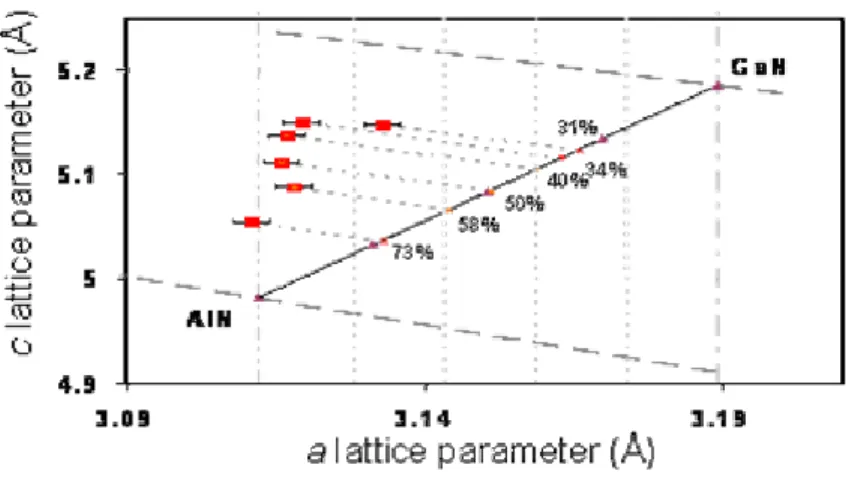
Figure 3.4: c versus a lattice parameter variation of AlxGa1-xN layers with x varying between 0.73 and 0.31. The thickness of layers is about 150 nm. The line between AlN and GaN corresponds to the expected behavior of fully relaxed AlxGa1-xN layers.
0 10 20 30
0 1 2
∆a/a0by RHEED(%)
time (sec) x = 0.21
0.28 0.34 0.530.4
0.58 0.73 0.85 1 (AlN)
(a)
0 10 20 30
0 1 2
∆a/a0by RHEED(%)
time (sec) x = 0.21
0.28 0.34 0.530.4
0.58 0.73 0.85 1 (AlN)
(a)
2.0 2.2 2.4 2.6 2.8
0.0 0.5 1.0 1.5 2.0 2.5
∆a/a0by RHEED (%)
∆a/a0by XRD (%)
(b)
2.0 2.2 2.4 2.6 2.8
0.0 0.5 1.0 1.5 2.0 2.5
∆a/a0by RHEED (%)
∆a/a0by XRD (%)
2.0 2.2 2.4 2.6 2.8
0.0 0.5 1.0 1.5 2.0 2.5
∆a/a0by RHEED (%)
∆a/a0by XRD (%)
(b)
Figure 3.5: a) In-plane lattice parameter variation as a function of time for GaN deposited on AlxGa1-xN with x varying between 0.21 and 1. b) In-plane lattice parameter variation as a function of GaN/AlxGa1-xN lattice mismatch. Dotted line is a guide.
To address this possibility, a set of AlxGa1-xN samples has been grown containing different Al concentrations. Then X-ray diffraction experiments, as shown in Figure 3.4, have been performed. The full line joining AlN and GaN illustrates the expected behavior of fully relaxed AlxGa1-xN layers. By contrast, the experimental points strongly deviate from this behavior, as an evidence that AlxGa1-xN layers, about 150 nm thick, are partially strained by the underlying AlN layer.
GaN QDs were then grown on this AlGaN buffers with concentrations shown in
3.5a. It shows that GaN elastic relaxation decreases for decreasing Al-content in AlxGa1-xN, consistent with the decreasing GaN/AlxGa1-xN lattice mismatch.
Furthermore, it shows that the critical thickness is unchanged as evidenced by the unchanged onset of GaN elastic relaxation, except for the lowest Al contents (28%
and 21%) for which no GaN QDs could be identified by AFM. In Figure 3.5b, GaN relaxation yield as extracted from RHEED data was plotted as a function of the GaN/AlGaN lattice mismatch as extracted from X-rays diffraction results in Figure 3.4.
Extrapolating the experimental values down to ∆a/a0GaN leads to suggest that the minimal lattice mismatch compatible with the occurrence of SK growth mode is 2 ± 0.1 %, of the same order as found for InGaAs/GaAs (~ 2%) [Leo93], GeSi/Si (1.4 %) [Eag90], PbSeTe/PbTe (1.6 %) [Pin98], and InGaN/GaN (1.4 - 1.8 %) [Ade00]. In conclusion the results show that it is possible to grow GaN QDs on AlGaN even with a Ga content of about 50 % due to the fact that the AlGaN layer is strained by the underlying Al substrate.
During this experiment great care was taken to grow AlGaN layers with suitable quality. For this the substrate temperature has been chosen higher than 730°C to enhance the mobility of Al-adatoms. As in case of GaN and AlN layers, metal-rich growth conditions are required, we took advantage of the surfactant properties of In which are discussed in more detail in reference [Mon03].
3.3 Rare earth doped GaN and AlN layers
MBE growth of RE doped GaN and AlN layers is a particularly new field. It is not clear, what is the incorporation rate of RE atoms into GaN in slightly Ga-rich and AlN in Al-rich growth conditions required for high quality layer growth.
Another problem of RE doping of nitride layers can be the creation of RE related defects, which reduces crystalline quality [Fil04]. These imperfections are expected to play an important role in RE excitation, which has to be avoided s


![Figure 3.2: Phase diagram indicating growth-modes in GaN heteroepitaxy on AlN. From [Mul01]](https://thumb-eu.123doks.com/thumbv2/1bibliocom/471381.74815/37.918.275.694.130.404/figure-phase-diagram-indicating-growth-modes-heteroepitaxy-mul01.webp)