The need to communicate securely over public channels led to the use of cryptography algorithms with asymmetric keys that commonly use a “hand-shake” mechanism, allowing the implementation of a “trust” system that ensures security of the transaction and the integrity of the data can be quarantined. as long as the algorithm can provide strong resistance to cryptographic attacks. Although asymmetric key cryptography algorithms provided the solution for public communications, the continued demand for higher bandwidth made their use inefficient, as the complexity of the algorithms required processing costs that caused latency differences. The analysis of symmetric cryptographic algorithms resulted in the creation of the Advanced Encryption Standard (AES), published by NIST in 2001.
Also the need for authentication and integrity of the transmitted information resulted in the creation of the AES-GCM mode that can authenticate a data stream (up to 68𝐺𝑏) in a reliable and efficient way. In this thesis, we designed and implemented an AES-GCM algorithm in VHDL in Xilinx Virtex-5 FPGA technology that performs authenticated encryption with a 256-bit encryption key. Our AES-GCM implementation uses a non-pipelined version of the AES core and requires 15 cycles to encrypt 128 bits of plaintext, which is the minimum encryption duration supported without pipelined.
Our implementation of the AES-GCM algorithm with AES key = 256 bit, initialization vector (IV) vector = 96 bit and a fully parallel GHASH multiplier on a Xilinx's Virtex-5 XC5VFX130T FPGA that is pin-to-pin compatible with the Space-grade Xilinx's Virtex-5QV FPGA requires 5% slices and 1% BRAMs.
INTRODUCTION
CRYPTOGRAPHY
AES - (Advanced Encryption Standard)
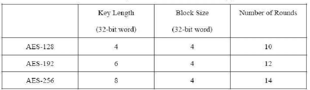
Key expansion is a basic operation that expands the initial key input to separate round keys. Each round key is one that is used in each round making it different from the others. This operation is what dictates how many rounds each block of data will be processed before the result is done, according to the size of the given key block.
GCM - (The Galois/Counter Mode)
Feedback mode means that the result of the current execution step of the algorithm is dependent on the previous step. This cipher-based MAC is called CMAC or Cipher Block Chaining MAC (CBC-MAC). In SP800-38C, NIST introduced a mode called CCM based on symmetric key block cipher where the block size is 128 bits. The throughput given by CTR mode is greater than that of CBC-MAC because in case of CTR the implementation can be done with pipeline techniques.
This can be achieved because the algorithm can be parallelized, making the multiplication process, which is the most demanding, complete in a single clock cycle. The tag is sent along with the encrypted data and is then used to ensure that the encrypted data belongs to someone who has access to the key.
MATHEMATICAL COMPONENTS OF AES-GCM
Basic functions
Least/Most Significant Bits - 𝐿𝑆𝐵𝑠(𝑥), 𝑀𝑆𝐵𝑠(𝑥): Given a bit string 𝑥 and an integer 𝑠 with 𝑠 ≤ 𝑙 a function of both 𝑙 𝑥 with 𝑀𝑆𝐵𝑠(𝑥) returning the most significant bits. left and 𝐿𝑆𝐵𝑠( 𝑥) rightmost parts.
AES functions
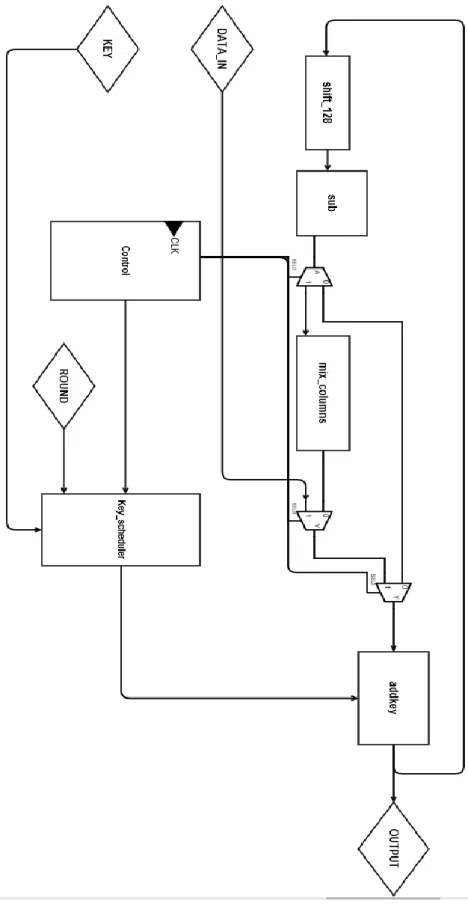
At each round, replacements and permutations are applied to the State array until the last round. MixColumns: A linear transformation is applied to each column based on the column's 4 bytes. AddRoundKey: Each byte in the State array is combined with a byte of the round key as it has been formed from the key expansion algorithm.
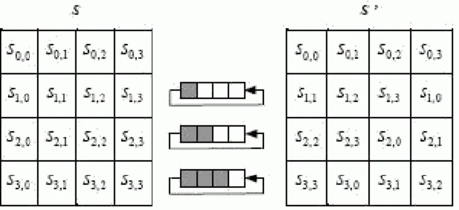
In this step, a non-linear transformation is applied to each byte with each byte from the S-field. The S-field is a look-up table (LUT) created by a 16x16 reversible matrix, with the 4 leftmost bits from each byte used as the row index and the 4 rightmost bits as the column index. In this step, each row of the State field is modified with the following pattern.
The second row is changed, moving each element i (byte) to the position i+1 and for i=3 then to i=0. The third row is changed with each element i (byte) moved to the position i+2. The fourth row is changed with each element i (byte) moved to the position i+3. Figure 4 shows the algorithm. This results in a fixed array by which each column is multiplied to obtain the new column (Figure 5).
Followed by the three previous steps in this step we apply an XOR operation to the 128 bits of the State array and 4*32 bit words from the round key. This algorithm extends the initial key so that a different round key is used in each round. For the following rounds, each word w[i] is constructed from the w[i-1] and the w[i-4] with a simple XOR in between.
GCM functions
DESIGN OF AES-GCM-256
AES Module
- Key Scheduler Module
- Control Unit
This output is used in an XOR operation with the feedback output of the first register after the second register which uses the result of the first register and so on. The output of the algorithm is a 128-bit round key which is used in an XOR operation with the plaintext to produce the round cipher. For the round key we use the first 4 registers for the odd number of rounds and the last 4 registers for the even number of rounds, which means we use a feedback mechanism for the 256-bit key.
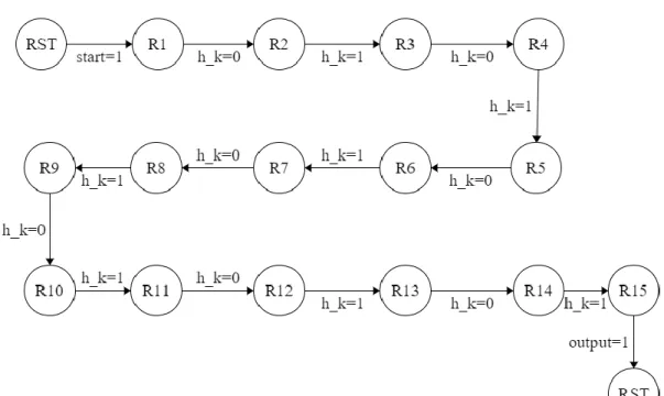
The control module for AES is a state machine consisting of 6 control indicators as output and 1 control as input. The process consists of a reset round "RST", 14 operation rounds from R1 to R14 and a competition round R15. The "start" control button is an external signal that initializes the encryption operation on the current input of data and key.
GCM Module
- GF multiplier
- GHASH
- GCTR
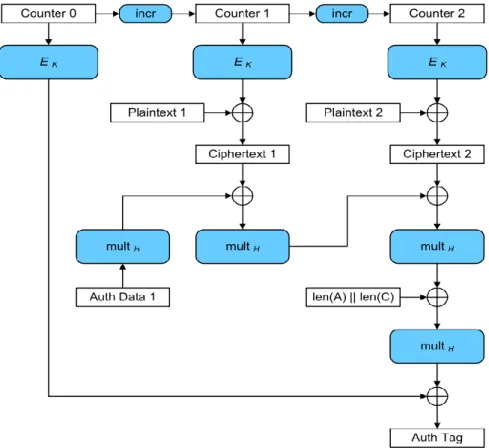
In Figure 10 we see a graphical illustration of the algorithm with two blocks of plain text and a single block with additional verified data as input. A major advantage of GCM is that the multiplication operation can be parallelized so that the final output can be produced in a radius of operational cycles from 128 to 1. Mastrovito proposed the use of a matrix𝑘 𝑥 𝑘called the multiplication array which can be created from the combination of 𝑎(𝑥)and 𝑥128+ 𝑥7 + 𝑥2+ 𝑥 + 1.
Its hardware implementation can calculate each 𝑐𝑖 using AND gates and a tree structure of XOR gates. This can result in the result of the multiplication process in just 1 clock, since each input is an output for an array, but 𝑍 calculates all its bits simultaneously. The main use of the 𝐺𝐹(2128) multiplier is in the 𝐺𝐻𝐴𝑆𝐻 function to compress ciphertext and additional authentication data into a single block.
The 𝐺𝐻𝐴𝑆𝐻 has a static parameter 𝐻 which is the hash key and is calculated by inserting the entry 0128 in AES and the key 𝐾. 𝐺𝐻𝐴𝑆𝐻 calculates a series of data blocks and the input depends on the output. Considering this, it is clear that most of 𝐺𝐻𝐴𝑆𝐻 the 𝐺𝐹(2128) multiplier needs to be as fast as possible, making the parallel version of 𝐺𝐹(2128) a one-way option.
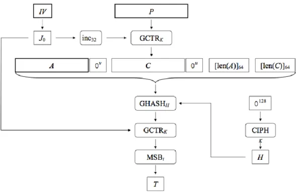
The GCM confidentiality mechanism is an alternative to the CTR method, which is called GCTR using an increasing function to obtain the required sequence of blocks. The first counter block is produced by incrementing a product block of the IV initialization vector. In step 1 we divide the input into a number of blocks where the last can be a full block or a non-empty partial block.
IMPLEMENTATION AND SIMULATION
- AES-256
- GF Multiplier
- GCM
- GCM control unit
- AES-GCM module
- Validation
- Test case 1
- Test case 2
- Test case 3
We implemented a series of AND and Although this is the largest combination path in our design, the total delay is a small fraction of the delay we would have if we used the multi-cycle version. For the purposes of this thesis, we have made some assumptions about the I/O mechanism, as it is a streaming data system and differences with different setups can change the buffer model.
The data stored: The initialization vector (IV – 96 bits) which needs 1 cycle, the key used (K – 256 bits) which needs 2 cycles, the least significant bits of the final plaintext (LSB_Last_Plain – 128 bits) which needs 1 cycle and the size of both ADD and plain text which is 64 bit for each and we stored it in the same register (AAD_size 64 bit, Plain_size 64 bit) which needs 1 final cycle. For each plaintext, we wait for the AES kernel to encrypt them before outputting the result and inserting it into the GHASH function. At the last steps we use the size of both ADD and plain text to calculate the final output which is the TAG.
Since the plaintext must be encoded and then the result multiplied, we need 15 clock cycles and 1 cycle to reset the AES module for the next input. Multiplexer u6 is responsible for the output of the module to be either digital or TAG. In Figure 22 we can see the simulation of a vector with 2 AAD blocks and 4 plain text blocks.
When the process is complete, the done signal becomes 1 and the mux changes the output to that of GHASH which is TAG. We achieved a minimum period of 4,392 ns with 16 clock cycles for processing a single plaintext block. But these improvements, which would allow processing of 68 Gbps in less than 10 seconds, are of minor importance since the buffer system cannot support speeds even close to that, albeit limiting the potential of the FPGA.
Test vector 1 is presented in Table 5, where we do not have any AAD, and the plaintext and key have zero values. Test vector 2 is presented in Table 6, where we have no AAD, but used null values for plaintext and key.