Figure B-0.
Table B-0.
Listing B-0.
Overview
The DSP has general-purpose and dedicated registers in each of its func- tional blocks. The register reference information for each functional block includes bit definitions, initialization values, and (for I/O processor regis- ters) memory mapped address. Information on each type of register is available at the following locations:
• “Core Status Registers” on page A-8
• “Computational Unit Registers” on page A-12
• “Program Sequencer Registers” on page A-16
• “Data Address Generator Registers” on page A-23
• “I/O Processor (Memory Mapped) Registers” on page B-2
When writing DSP programs, it is often necessary to set, clear, or test bits in the DSP’s registers. While these bit operations can all be done by refer- ring to the bit’s location within a register or (for some operations) the register’s address with a hexadecimal number, it is much easier to use sym- bols that correspond to the bit’s or register’s name. For convenience and consistency, Analog Devices provides a header file that provides these bit and register definitions. For more information, see the “Register & Bit
#Defines File (def219x.h)” on page A-26 and “Register and Bit #define File (def2191.h)” on page B-109.
I/O Processor (Memory Mapped) Registers
I/O Processor (Memory Mapped) Registers
The DSP’s memory map includes the following groups of I/O processor registers:
• “Clock and System Control Registers” on page B-14
• “Interrupt Controller Registers” on page B-20
• “DMA Controller Registers” on page B-24
• “SPORT Registers” on page B-31
• “Serial Peripheral Interface Registers” on page B-53
• “UART Registers” on page B-65
• “Timer Registers” on page B-82
• “Programmable Flag Registers” on page B-89
• “External Memory Interface Registers” on page B-91
• “Host Port Registers” on page B-101
The I/O processor registers are accessible as part of the DSP’s memory map. Table B-1 on page B-3 lists the I/O processor’s memory mapped registers in address order and provides a cross reference to a description of each register. These registers occupy addresses 0x00 through 0xFF of the memory map and control I/O operations, including:
• External port DMA
• Link port DMA
• Serial port DMA
I/O processor registers have a one cycle effect latency (changes take effect on the second cycle after the change).Because the I/O processor’s registers are part of the DSP’s I/O memory map, buses access these registers as locations in I/O memory. While these registers act as memory mapped locations, they are separate from the DSP’s internal memory.
To read or write I/O processor registers, programs must use the Io( ) instruction. The following example code shows a value being transferred from the AX0 register to the DMACW_CP register in I/O memory. The IOPG register is loaded to select the correct page in I/O memory. Because the page and address are necessary for accessing any I/O memory register, the I/O memory map in Table B-1 shows these as IOPG:Address.
iopg = Memory_DMA_Controller_Page; /* set the I/O mem page */
ax0 = WR_DMA_WORD_CONFIG; /* loads ax0 with the cfg word */
io(DMACW_CP) = ax0; /* loads DMACW_CP with the cfg word */
The register names for I/O processor registers are not part of the DSP’s assembly syntax. To ease access to these registers, programs should use the
#include command to incorporate a file containing the registers’ symbolic names and addresses. An example #include file appears in the “Register and Bit #define File (def2191.h)” on page B-109.
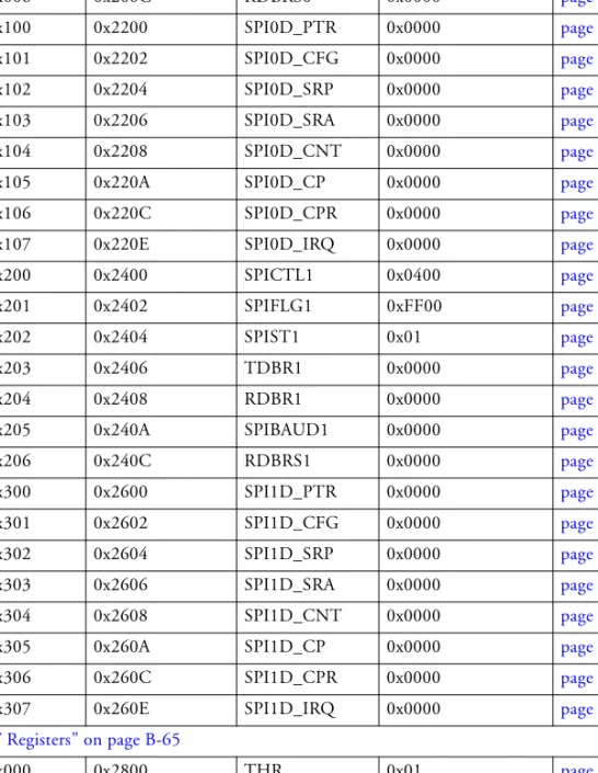
Table B-1. I/O Processor Registers Memory Map
DSP I/O Address
(IOPG:Address) Host I/O Address1 (on HA16–HAD1)
Register Name Initialization After Reset
Page Cross Reference
“Clock and System Control Registers” on page B-14
0x00:0x200 0x0400 PLLCTL 0x0010 page B-14
0x00:0x201 0x0402 LOCKCNT ni page B-17
0x00:0x202 0x0404 SWRST ni page B-17
0x00:0x203 0x0406 NXTSCR 0x0000 page B-17
0x00:0x204 0x0408 SYSCR 0x0000 page B-19
“Interrupt Controller Registers” on page B-20
0x01:0x200 0x0C00 IPR0 Per interrupt request page B-20
I/O Processor (Memory Mapped) Registers
0x01:0x202 0x0C04 IPR2 Per interrupt request page B-20 0x01:0x203 0x0C06 IPR3 Per interrupt request page B-20 0x01:0x204 0x0C08 INTRD0 Per interrupt request page B-23 0x01:0x205 0x0C0A INTRD1 Per interrupt request page B-23 0x01:0x206 0x0C0C INTRD2 Per interrupt request page B-23 0x01:0x207 0x0C0E INTRD3 Per interrupt request page B-23 0x01:0x208 0x0C0F INTRD4 Per interrupt request page B-23 0x01:0x209 0x0C12 INTRD5 Per interrupt request page B-23 0x01:0x20A 0x0C14 INTRD6 Per interrupt request page B-23 0x01:0x20B 0x0C16 INTRD7 Per interrupt request page B-23 0x01:0x20C 0x0C18 INTRD8 Per interrupt request page B-23 0x01:0x20D 0x0C1A INTRD9 Per interrupt request page B-23 0x01:0x20E 0x0C1C INTRD10 Per interrupt request page B-23 0x01:0x20F 0x0C1E INTRD11 Per interrupt request page B-23
“DMA Controller Registers” on page B-24
0x02:0x100 0x1200 DMACW_PTR 0x0000 page B-24
0x02:0x101 0x1202 DMACW_CFG 0x0000 page B-24
0x02:0x102 0x1204 DMACW_SRP 0x0000 page B-26
0x02:0x103 0x1206 DMACW_SRA 0x0000 page B-26
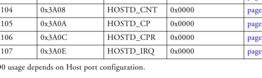
0x02:0x104 0x1208 DMACW_CNT 0x0000 page B-26
0x02:0x105 0x120A DMACW_CP 0x0000 page B-27
0x02:0x106 0x120C DMACW_CPR 0x0000 page B-27
0x02:0x107 0x120E DMACW_IRQ 0x0000 page B-27
0x02:0x180 0x1300 DMACR_PTR 0x0000 page B-28
0x02:0x181 0x1302 DMACR_CFG 0x0000 page B-28
0x02:0x182 0x1304 DMACR_SRP 0x0000 page B-29
0x02:0x183 0x1306 DMACR_SRA 0x0000 page B-29
Table B-1. I/O Processor Registers Memory Map (Cont’d)
DSP I/O Address
(IOPG:Address) Host I/O Address1 (on HA16–HAD1)
Register Name Initialization After Reset
Page Cross Reference
0x02:0x185 0x130A DMACR_CP 0x0000 page B-30
0x02:0x186 0x130C DMACR_CPR 0x0000 page B-30
0x02:0x00187 0x130E DMACR_IRQ 0x0000 page B-30
“SPORT Registers” on page B-31
0x02:0x200 0x1400 SP0_TCR 0x0000 page B-31
0x02:0x201 0x1402 SP0_RCR 0x0000 page B-33
0x02:0x202 0x1404 SP0_TX 0x0000 page B-34
0x02:0x203 0x1406 SP0_RX 0x0000 page B-34
0x02:0x204 0x1408 SP0_TSCKDIV 0x0000 page B-35
0x02:0x205 0x140A SP0_RSCKDIV 0x0000 page B-35
0x02:0x206 0x140C SP0_TFSDIV 0x0000 page B-36
0x02:0x207 0x140E SP0_RFSDIV 0x0000 page B-35
0x02:0x208 0x1410 SP0_STATR 0x0000 page B-36
0x02:0x209 0x1412 SP0_MTCS0 0x0000 page B-38
0x02:0x20A 0x1414 SP0_MTCS1 0x0000 page B-38
0x02:0x20B 0x1416 SP0_MTCS2 0x0000 page B-38
0x02:0x20C 0x1418 SP0_MTCS3 0x0000 page B-38
0x02:0x20D 0x141A SP0_MTCS4 0x0000 page B-38
0x02:0x20E 0x141C SP0_MTCS5 0x0000 page B-38
0x02:0x20F 0x141E SP0_MTCS6 0x0000 page B-38
0x02:0x210 0x1420 SP0_MTCS7 0x0000 page B-38
0x02:0x211 0x1422 SP0_MRCS0 0x0000 page B-39
0x02:0x212 0x1424 SP0_MRCS1 0x0000 page B-39
0x02:0x213 0x1426 SP0_MRCS2 0x0000 page B-39
0x02:0x214 0x1428 SP0_MRCS3 0x0000 page B-39
0x02:0x215 0x142A SP0_MRCS4 0x0000 page B-39
Table B-1. I/O Processor Registers Memory Map (Cont’d)
DSP I/O Address
(IOPG:Address) Host I/O Address1 (on HA16–HAD1)
Register Name Initialization After Reset
Page Cross Reference
I/O Processor (Memory Mapped) Registers
0x02:0x218 0x1430 SP0_MRCS7 0x0000 page B-39
0x02:0x219 0x1432 SP0_MCMC1 0x0000 page B-40
0x02:0x21A 0x1434 SP0_MCMC2 0x0000 page B-40
0x02:0x300 0x1600 SP0DR_PTR 0x0000 page B-43
0x02:0x301 0x1602 SP0DR_CFG 0x0000 page B-43
0x02:0x302 0x1604 SP0DR_SRP 0x0000 page B-43
0x02:0x303 0x1606 SP0DR_SRA 0x0000 page B-46
0x02:0x304 0x1608 SP0DR_CNT 0x0000 page B-46
0x02:0x305 0x160A SP0DR_CP 0x0000 page B-46
0x02:0x306 0x160C SP0DR_CPR 0x0000 page B-47
0x02:0x307 0x160E SP0DR_IRQ 0x0000 page B-47
0x02:0x380 0x1700 SP0DT_PTR 0x0000 page B-48
0x02:0x381 0x1702 SP0DT_CFG 0x0000 page B-48
0x02:0x382 0x1704 SP0DT_SRP 0x0000 page B-49
0x02:0x383 0x1706 SP0DT_SRA 0x0000 page B-49
0x02:0x384 0x1708 SP0DT_CNT 0x0000 page B-49
0x02:0x385 0x170A SP0DT_CP 0x0000 page B-50
0x02:0x386 0x170C SP0DT_CPR 0x0000 page B-51
0x02:0x387 0x170E SP0DT_IRQ 0x0000 page B-51
0x03:0x000 0x1800 SP1_TCR 0x0000 page B-31
0x03:0x001 0x1802 SP1_RCR 0x0000 page B-33
0x03:0x002 0x1804 SP1_TX 0x0000 page B-34
0x03:0x003 0x1806 SP1_RX 0x0000 page B-34
0x03:0x004 0x1808 SP1_TSCKDIV 0x0000 page B-35
0x03:0x005 0x180A SP1_RSCKDIV 0x0000 page B-35
0x03:0x006 0x180C SP1_TFSDIV 0x0000 page B-36
0x03:0x007 0x180E SP1_RFSDIV 0x0000 page B-35
Table B-1. I/O Processor Registers Memory Map (Cont’d)
DSP I/O Address
(IOPG:Address) Host I/O Address1 (on HA16–HAD1)
Register Name Initialization After Reset
Page Cross Reference
0x03:0x009 0x1812 SP1_MTCS0 0x0000 page B-38
0x03:0x00A 0x1814 SP1_MTCS1 0x0000 page B-38
0x03:0x00B 0x1816 SP1_MTCS2 0x0000 page B-38
0x03:0x00C 0x1818 SP1_MTCS3 0x0000 page B-38
0x03:0x00D 0x181A SP1_MTCS4 0x0000 page B-38
0x03:0x00E 0x181C SP1_MTCS5 0x0000 page B-38
0x03:0x00F 0x181E SP1_MTCS6 0x0000 page B-38
0x03:0x010 0x1820 SP1_MTCS7 0x0000 page B-38
0x03:0x011 0x1822 SP1_MRCS0 0x0000 page B-39
0x03:0x012 0x1824 SP1_MRCS1 0x0000 page B-39
0x03:0x013 0x1826 SP1_MRCS2 0x0000 page B-39
0x03:0x014 0x1828 SP1_MRCS3 0x0000 page B-39
0x03:0x015 0x182A SP1_MRCS4 0x0000 page B-39
0x03:0x016 0x182C SP1_MRCS5 0x0000 page B-39
0x03:0x017 0x182E SP1_MRCS6 0x0000 page B-39
0x03:0x018 0x1830 SP1_MRCS7 0x0000 page B-39
0x03:0x019 0x1832 SP1_MCMC1 0x0000 page B-40
0x03:0x01A 0x1834 SP1_MCMC2 0x0000 page B-40
0x03:0x100 0x1A00 SP1DR_PTR 0x0000 page B-43
0x03:0x101 0x1A02 SP1DR_CFG 0x0000 page B-43
0x03:0x102 0x1A04 SP1DR_SRP 0x0000 page B-43
0x03:0x103 0x1A06 SP1DR_SRA 0x0000 page B-46
0x03:0x104 0x1A08 SP1DR_CNT 0x0000 page B-46
0x03:0x105 0x1A0A SP1DR_CP 0x0000 page B-46
0x03:0x106 0x1A0C SP1DR_CPR 0x0000 page B-47
0x03:0x107 0x1A0E SP1DR_IRQ 0x0000 page B-47
Table B-1. I/O Processor Registers Memory Map (Cont’d)
DSP I/O Address
(IOPG:Address) Host I/O Address1 (on HA16–HAD1)
Register Name Initialization After Reset
Page Cross Reference
I/O Processor (Memory Mapped) Registers
0x03:0x182 0x1A14 SP1DT_SRP 0x0000 page B-49
0x03:0x183 0x1A16 SP1DT_SRA 0x0000 page B-49
0x03:0x184 0x1A18 SP1DT_CNT 0x0000 page B-49
0x03:0x185 0x1A1A SP1DT_CP 0x0000 page B-50
0x03:0x186 0x1A1C SP1DT_CPR 0x0000 page B-51
0x03:0x187 0x1A1E SP1DT_IRQ 0x0000 page B-51
0x03:0x200 0x1C00 SP2_TCR 0x0000 page B-31
0x03:0x201 0x1C02 SP2_RCR 0x0000 page B-33
0x03:0x202 0x1C04 SP2_TX 0x0000 page B-34
0x03:0x203 0x1C06 SP2_RX 0x0000 page B-34
0x03:0x204 0x1C08 SP2_TSCKDIV 0x0000 page B-35
0x03:0x205 0x1C0A SP2_RSCKDIV 0x0000 page B-35
0x03:0x206 0x1C0C SP2_TFSDIV 0x0000 page B-36
0x03:0x207 0x1C0E SP2_RFSDIV 0x0000 page B-35
0x03:0x208 0x1C10 SP2_STATR 0x0000 page B-36
0x03:0x209 0x1C12 SP2_MTCS0 0x0000 page B-38
0x03:0x20A 0x1C14 SP2_MTCS1 0x0000 page B-38
0x03:0x20B 0x1C16 SP2_MTCS2 0x0000 page B-38
0x03:0x20C 0x1C18 SP2_MTCS3 0x0000 page B-38
0x03:0x20D 0x1C1A SP2_MTCS4 0x0000 page B-38
0x03:0x20E 0x1C1C SP2_MTCS5 0x0000 page B-38
0x03:0x20F 0x1C1E SP2_MTCS6 0x0000 page B-38
0x03:0x210 0x1C20 SP2_MTCS7 0x0000 page B-38
0x03:0x211 0x1C22 SP2_MRCS0 0x0000 page B-39
0x03:0x212 0x1C24 SP2_MRCS1 0x0000 page B-39
0x03:0x213 0x1C26 SP2_MRCS2 0x0000 page B-39
0x03:0x214 0x1C28 SP2_MRCS3 0x0000 page B-39
Table B-1. I/O Processor Registers Memory Map (Cont’d)
DSP I/O Address
(IOPG:Address) Host I/O Address1 (on HA16–HAD1)
Register Name Initialization After Reset
Page Cross Reference
0x03:0x216 0x1C2C SP2_MRCS5 0x0000 page B-39
0x03:0x217 0x1C2E SP2_MRCS6 0x0000 page B-39
0x03:0x218 0x1C30 SP2_MRCS7 0x0000 page B-39
0x03:0x219 0x1C32 SP2_MCMC1 0x0000 page B-40
0x03:0x21A 0x1C34 SP2_MCMC2 0x0000 page B-40
0x03:0x300 0x1E00 SP2DR_PTR 0x0000 page B-43
0x03:0x301 0x1E02 SP2DR_CFG 0x0000 page B-43
0x03:0x302 0x1E04 SP2DR_SRP 0x0000 page B-43
0x03:0x303 0x1E06 SP2DR_SRA 0x0000 page B-46
0x03:0x304 0x1E08 SP2DR_CNT 0x0000 page B-46
0x03:0x305 0x1E0A SP2DR_CP 0x0000 page B-46
0x03:0x306 0x1E0C SP2DR_CPR 0x0000 page B-47
0x03:0x307 0x1E0E SP2DR_IRQ 0x0000 page B-47
0x03:0x380 0x1E10 SP2DT_PTR 0x0000 page B-48
0x03:0x381 0x1E12 SP2DT_CFG 0x0000 page B-48
0x03:0x382 0x1E14 SP2DT_SRP 0x0000 page B-49
0x03:0x383 0x1E16 SP2DT_SRA 0x0000 page B-49
0x03:0x384 0x1E18 SP2DT_CNT 0x0000 page B-49
0x03:0x385 0x1E1A SP2DT_CP 0x0000 page B-50
0x03:0x386 0x1E1C SP2DT_CPR 0x0000 page B-51
0x03:0x387 0x1E1E SP2DT_IRQ 0x0000 page B-51
“Serial Peripheral Interface Registers” on page B-53
0x04:0x000 0x2000 SPICTL0 0x0400 page B-53
0x04:0x001 0x2002 SPIFLG0 0xFF00 page B-56
0x04:0x002 0x20024 SPIST0 0x01 page B-58
0x04:0x003 0x2006 TDBR0 0x0000 page B-59
Table B-1. I/O Processor Registers Memory Map (Cont’d)
DSP I/O Address
(IOPG:Address) Host I/O Address1 (on HA16–HAD1)
Register Name Initialization After Reset
Page Cross Reference
I/O Processor (Memory Mapped) Registers
0x04:0x006 0x200C RDBRS0 0x0000 page B-60
0x04:0x100 0x2200 SPI0D_PTR 0x0000 page B-61
0x04:0x101 0x2202 SPI0D_CFG 0x0000 page B-61
0x04:0x102 0x2204 SPI0D_SRP 0x0000 page B-63
0x04:0x103 0x2206 SPI0D_SRA 0x0000 page B-63
0x04:0x104 0x2208 SPI0D_CNT 0x0000 page B-63
0x04:0x105 0x220A SPI0D_CP 0x0000 page B-63
0x04:0x106 0x220C SPI0D_CPR 0x0000 page B-64
0x04:0x107 0x220E SPI0D_IRQ 0x0000 page B-64
0x04:0x200 0x2400 SPICTL1 0x0400 page B-53
0x04:0x201 0x2402 SPIFLG1 0xFF00 page B-56
0x04:0x202 0x2404 SPIST1 0x01 page B-58
0x04:0x203 0x2406 TDBR1 0x0000 page B-59
0x04:0x204 0x2408 RDBR1 0x0000 page B-60
0x04:0x205 0x240A SPIBAUD1 0x0000 page B-60
0x04:0x206 0x240C RDBRS1 0x0000 page B-60
0x04:0x300 0x2600 SPI1D_PTR 0x0000 page B-61
0x04:0x301 0x2602 SPI1D_CFG 0x0000 page B-61
0x04:0x302 0x2604 SPI1D_SRP 0x0000 page B-63
0x04:0x303 0x2606 SPI1D_SRA 0x0000 page B-63
0x04:0x304 0x2608 SPI1D_CNT 0x0000 page B-63
0x04:0x305 0x260A SPI1D_CP 0x0000 page B-63
0x04:0x306 0x260C SPI1D_CPR 0x0000 page B-64
0x04:0x307 0x260E SPI1D_IRQ 0x0000 page B-64
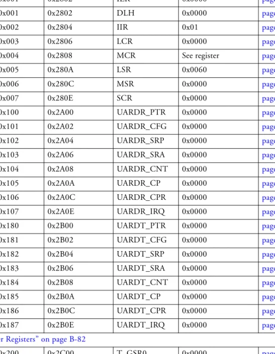
“UART Registers” on page B-65
0x05:0x000 0x2800 THR 0x01 page B-66
0x05:0x000 0x2800 RBR 0x0000 page B-67
Table B-1. I/O Processor Registers Memory Map (Cont’d)
DSP I/O Address
(IOPG:Address) Host I/O Address1 (on HA16–HAD1)
Register Name Initialization After Reset
Page Cross Reference
0x05:0x001 0x2802 IER 0x0000 page B-67
0x05:0x001 0x2802 DLH 0x0000 page B-68
0x05:0x002 0x2804 IIR 0x01 page B-70
0x05:0x003 0x2806 LCR 0x0000 page B-71
0x05:0x004 0x2808 MCR See register page B-72
0x05:0x005 0x280A LSR 0x0060 page B-73
0x05:0x006 0x280C MSR 0x0000 page B-74
0x05:0x007 0x280E SCR 0x0000 page B-74
0x05:0x100 0x2A00 UARDR_PTR 0x0000 page B-75
0x05:0x101 0x2A02 UARDR_CFG 0x0000 page B-75
0x05:0x102 0x2A04 UARDR_SRP 0x0000 page B-77
0x05:0x103 0x2A06 UARDR_SRA 0x0000 page B-77
0x05:0x104 0x2A08 UARDR_CNT 0x0000 page B-77
0x05:0x105 0x2A0A UARDR_CP 0x0000 page B-78
0x05:0x106 0x2A0C UARDR_CPR 0x0000 page B-78
0x05:0x107 0x2A0E UARDR_IRQ 0x0000 page B-78
0x05:0x180 0x2B00 UARDT_PTR 0x0000 page B-79
0x05:0x181 0x2B02 UARDT_CFG 0x0000 page B-79
0x05:0x182 0x2B04 UARDT_SRP 0x0000 page B-79
0x05:0x183 0x2B06 UARDT_SRA 0x0000 page B-80
0x05:0x184 0x2B08 UARDT_CNT 0x0000 page B-80
0x05:0x185 0x2B0A UARDT_CP 0x0000 page B-80
0x05:0x186 0x2B0C UARDT_CPR 0x0000 page B-80
0x05:0x187 0x2B0E UARDT_IRQ 0x0000 page B-80
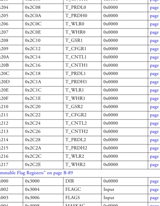
“Timer Registers” on page B-82
0x05:0x200 0x2C00 T_GSR0 0x0000 page B-82
Table B-1. I/O Processor Registers Memory Map (Cont’d)
DSP I/O Address
(IOPG:Address) Host I/O Address1 (on HA16–HAD1)
Register Name Initialization After Reset
Page Cross Reference
I/O Processor (Memory Mapped) Registers
0x05:0x203 0x2C06 T_CNTH0 0x0000 page B-84
0x05:0x204 0x2C08 T_PRDL0 0x0000 page B-86
0x05:0x205 0x2C0A T_PRDH0 0x0000 page B-86
0x05:0x206 0x2C0C T_WLR0 0x0000 page B-87
0x05:0x207 0x2C0E T_WHR0 0x0000 page B-87
0x05:0x208 0x2C10 T_GSR1 0x0000 page B-82
0x05:0x209 0x2C12 T_CFGR1 0x0000 page B-84
0x05:0x20A 0x2C14 T_CNTL1 0x0000 page B-84
0x05:0x20B 0x2C16 T_CNTH1 0x0000 page B-84
0x05:0x20C 0x2C18 T_PRDL1 0x0000 page B-86
0x05:0x20D 0x2C1A T_PRDH1 0x0000 page B-86
0x05:0x20E 0x2C1C T_WLR1 0x0000 page B-87
0x05:0x20F 0x2C1E T_WHR1 0x0000 page B-87
0x05:0x210 0x2C20 T_GSR2 0x0000 page B-82
0x05:0x211 0x2C22 T_CFGR2 0x0000 page B-84
0x05:0x212 0x2C24 T_CNTL2 0x0000 page B-84
0x05:0x213 0x2C26 T_CNTH2 0x0000 page B-84
0x05:0x214 0x2C28 T_PRDL2 0x0000 page B-86
0x05:0x215 0x2C2A T_PRDH2 0x0000 page B-86
0x05:0x216 0x2C2C T_WLR2 0x0000 page B-87
0x05:0x217 0x2C2E T_WHR2 0x0000 page B-87
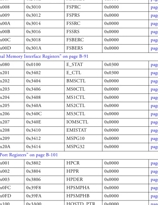
“Programmable Flag Registers” on page B-89
0x06:0x000 0x3000 DIR 0x0000 page B-89
0x06:0x002 0x3004 FLAGC Input page B-89
0x06:0x003 0x3006 FLAGS Input page B-89
0x06:0x004 0x3008 MASKAC 0x0000 page B-89
0x06:0x005 0x300A MASKAS 0x0000 page B-89
Table B-1. I/O Processor Registers Memory Map (Cont’d)
DSP I/O Address
(IOPG:Address) Host I/O Address1 (on HA16–HAD1)
Register Name Initialization After Reset
Page Cross Reference
0x06:0x007 0x300E MASKBS 0x0000 page B-89
0x06:0x008 0x3010 FSPRC 0x0000 page B-90
0x06:0x009 0x3012 FSPRS 0x0000 page B-90
0x06:0x00A 0x3014 FSSRC 0x0000 page B-91
0x06:0x00B 0x3016 FSSRS 0x0000 page B-91
0x06:0x00C 0x3018 FSBERC 0x0000 page B-91
0x06:0x00D 0x301A FSBERS 0x0000 page B-91
“External Memory Interface Registers” on page B-91
0x00:0x080 0x0100 E_STAT 0x0300 page B-92
0x06:0x201 0x3402 E_CTL 0x0300 page B-93
0x06:0x202 0x3404 BMSCTL 0x0000 page B-94
0x06:0x203 0x3406 MS0CTL 0x0000 page B-96
0x06:0x204 0x3408 MS1CTL 0x0000 page B-96
0x06:0x205 0x340A MS2CTL 0x0000 page B-96
0x06:0x206 0x340C MS3CTL 0x0000 page B-96
0x06:0x207 0x340E IOMSCTL 0x0000 page B-97
0x06:0x208 0x3410 EMISTAT 0x0000 page B-97
0x06:0x209 0x3412 MSPG10 0x0000 page B-100
0x06:0x20A 0x3414 MSPG32 0x0000 page B-100
“Host Port Registers” on page B-101
0x07:0x001 0x3802 HPCR 0x0000 page B-101
0x07:0x002 0x3804 HPPR 0x0000 page B-104
0x07:0x003 0x3806 HPDER 0x0000 page B-104
0x07:0x0FC 0x39F8 HPSMPHA 0x0000 page B-104
0x07:0x0FD 0x39FA HPSMPHB 0x0000 page B-104
0x07:0x100 0x3A00 HOSTD_PTR 0x0000 page B-105
Table B-1. I/O Processor Registers Memory Map (Cont’d)
DSP I/O Address
(IOPG:Address) Host I/O Address1 (on HA16–HAD1)
Register Name Initialization After Reset
Page Cross Reference
Clock and System Control Registers
Clock and System Control Registers
Clock and System Control group of I/P registers include:
• “PLL Control (PLLCTL) Register” on page B-14
• “PLL Lock Counter (LOCKCNT) Register” on page B-17
• “Software Reset (SWRST) Register” on page B-17
• “Next System Configuration (NXTSCR) Register” on page B-17
• “System Configuration (SYSCR) Register” on page B-19 PLL Control (PLLCTL) Register
The PLL Control (PLLCTL) register lets systems select and change the DSP’s core clock (CCLK) frequency and select powerdown modes. The PLL multiplies the clock frequency of the input clock with a programma- ble ratio. The PLL Control register address is 0x00:0x200.
0x07:0x103 0x3A06 HOSTD_SRA 0x0000 page B-107
0x07:0x104 0x3A08 HOSTD_CNT 0x0000 page B-107
0x07:0x105 0x3A0A HOSTD_CP 0x0000 page B-107
0x07:0x106 0x3A0C HOSTD_CPR 0x0000 page B-108
0x07:0x107 0x3A0E HOSTD_IRQ 0x0000 page B-108
1 HAD0 usage depends on Host port configuration.
Table B-1. I/O Processor Registers Memory Map (Cont’d)
DSP I/O Address
(IOPG:Address) Host I/O Address1 (on HA16–HAD1)
Register Name Initialization After Reset
Page Cross Reference
At reset, the PLL starts in BYPASS mode, running the CCLK clock directly from CLKIN. The reset must be active at least four clock cycle to allow full initialization of the synchronizer chain. After the PLL is locked, software can switch to a clock multiplier mode.
Figure B-1 provides bit descriptions for the register.
15 14 13 12 11 10 9 8 7 6 5 4 3 2 1 0
0 0 0 0 0 0 0 0 0 0 0 1 0 0 0 0 Reset = 0x0010
DF (Divide Frequency)
00/01=No PLL, 10=CLKIN to PLL, 11=CLKIN/2 to PLL
PO (PLL Off)
0= PLL on, 1= PLL off STOPALL (Stop All PLL Output)
0=PLL output, 1=CCLK and HCLK high
STOPCK (Stop Core Clock) 0=CCLK output, 1=CCLK high IOSEL (Core:Peripheral Clock Ratio)
0=HCLK=CCLK, 1=HCLK=CCLK/2 PDWN (Powerdown)
0=run, 1=Powerdown all CKOUTEN (CLKOUT Enable)
0=CLKOUT=0, 1=CLKOUT=HCLK DIV2 (Divide CLKIN /2 In Bypass Enable)
0=no divide, 1=CCLK=CLKIN/2 in Bypass
BYPASS (Bypass PLL Multiplier) 0=Multiplier mode, 1=Bypass mode MSEL4–0 (CLKIN Multiply Ratio)
00 = 0 to 15, 01 =16 to 31, 10 = 0.5 to 15.5, 11 = 0 to 15 MSEL5 (Second Stage Multiplier Enable) MSEL6 (Output Multiplier Enable)
Figure B-1. PLL Control (PLLCTL) Register Bits
Clock and System Control Registers
Refer to “Using The PLL Control (PLLCTL) Register” on page 14-35 for more information.
PLL Lock Counter (LOCKCNT) Register
The Lock Counter is a 10-bit register. The register address is 0x00:0x201.
The process of changing the multiplication factor of the PLL takes a cer- tain number of cycles, and therefore a Lock Counter is required in order to calculate when the PLL is locked to the new ratio. The value of the Lock Counter depends on the frequency (the higher the capacitor must be charged, the longer is the time required to lock). At power-up, the Lock Counter has to be initialized. Therefore, during reset, the lock signal is forced and set active indicating that the PLL is locked even though this may not be true. The reset pulse must be long enough to guarantee that the PLL is effectively locked at the end of the reset sequence or the soft- ware must wait before switching the clock source to the PLL output.
Software Reset (SWRST) Register
The Software Reset Register is write-only. Its address is 0x00:0x202. The DSP core software reset is initiated by the DSP core by writing 0x07 into the Software Reset (SWR) bits 2–0 in the Software Control Register. Thus, value “7” triggers SW Reset, values 0–6 specify no software reset. Bits 3 through 15 are set to 0.
If bits 2–0 are set, the reset affects only the state of the core and most of the peripherals. It does not make use of the hardware reset timer and logic and does not reset the PLL and PLL control register.
A software reset of the peripheral will cause loss of state and immediate termination of DMA processing.
Next System Configuration (NXTSCR) Register This register address is 0x00:0x203.
During normal chip operation, reset parameters may be written by the
Clock and System Control Registers
reset. A subsequent software reset updates the state of the System Config- uration register with the contents of the Next System Configuration register, and will then be allowed to propagate through to the register out- put drivers and distributed to DSP core and peripherals. For bit
descriptions, see Figure B-2 on page B-18.
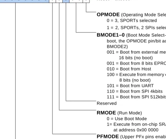
The reset state is initialized during hardware reset from boot mode pins. These bits are read-write during normal chip operation.15 14 13 12 11 10 9 8 7 6 5 4 3 2 1 0
0 0 0 0 0 0 0 0 0 0 0 0 0 0 0 0 Reset = 0x0000
OPMODE (Operating Mode Select) 0 = 3, SPORTs selected 1 =2, SPORTs, 2 SPIs selected BMODE1–0 (Boot Mode Select—at
boot, the OPMODE pin/bit acts as BMODE2)
001 = Boot from external memory 16 bits (no boot)
001 = Boot from 8 bits EPROM 010 = Boot from Host
100 = Execute from memory external 8 bits (no boot)
101 = Boot from UART 110 = Boot from SPI 4kbits 111 = Boot from SPI 512kbits Reserved
RMODE (Run Mode) 0 = Use Boot Mode
1= Execute from on-chip SRAM at address 0x00 0000 PFMODE (Upper PFx pins enable)
0 = Disable PF15–8 (16-bit bus) 1 = Enable PF15–8 (8-bit bus) Reserved
Figure B-2. Next System Configuration (NXTSCR) Register Bits
System Configuration (SYSCR) Register
The System Configuration register is a read-write register. Its address is
0x00:0x204.
A software reset will update the state of the System Configuration register with the contents of the Next System Configuration register, and will then be allowed to propagate through to the register output drivers and distrib- uted to the DSP core and peripherals. For information on the bits in this register (which are the same as the NXTSCR register), refer to Figure B-2.
The OPMODE pin is a dedicated mode control pin, it is typically used to select between one serial port or two SPI ports. During boot, the OPMODE pin serves as the BMODE2 pin.
The BMODE1–0 pins are the dedicated mode control pins. The pins and the corresponding bits in the System Configuration register configure the boot mode that is employed following hardware reset or software reset.
Interrupt Controller Registers
Interrupt Controller Registers
The Interrupt Controller module (IRQ) combines and prioritizes inter- rupt sources from the various peripherals. The peripheral interrupt controller module is a generic module used to combine and prioritize 16 interrupt sources into 12 interrupt requests. The module includes four configuration registers that individually define the priority of interrupt sources. The module also includes twelve interrupt read registers, each register being associated with one of the interrupt request. The Interrupt Controller Registers are:
• “Interrupt Priority (IPRx) Registers” on page B-20
• “Interrupt Source (INTRDx) Registers” on page B-23 Interrupt Priority (IPRx) Registers
There are four interrupt priority registers (which are part of the peripheral interrupt controller module). These registers have the following addresses:
IPR0 0x01:0x200 IPR1 0x01:0x201 IPR2 0x01:0x202 IPR3 0x01:0x203
As shown in Figure B-3, Figure B-4, Figure B-5, and Figure B-6, the IPRx registers individually define the priority of interrupt sources. Each IPRx register is a 16-bit peripheral memory mapped register which is divided into four-bit priority fields, each associated to one interrupt source. The priority level is defined from 0 to 11, 0 being the highest priority and 11 being the lowest. The interrupt request of priority 0 is connected to inter- rupt 4 of the DSP core and the interrupt request of priority 11 is
connected to interrupt 15 of the DSP core.
An interrupt source is configured and applied to one of the interrupt requests line as described in Table B-2.
15 14 13 12 11 10 9 8 7 6 5 4 3 2 1 0
0 0 1 1 0 0 1 0 0 0 0 1 0 0 0 0 Reset = 0x3210
HOSTIP (Host interrupt priority) SP0RXIP (SPORT0 RX interrupt priority) SP0TXIP (SPORT0 TX interrupt priority) SP1RXIP (SPORT1 RX interrupt priority)
Figure B-3. Interrupt Priority Register 0 (IPR0) Bits
15 14 13 12 11 10 9 8 7 6 5 4 3 2 1 0
0 1 1 1 0 1 1 0 0 1 0 1 0 1 0 0 Reset = 0x7654
SP1TXIP (SPORT1 TX interrupt priority) SP2RXIP (SPORT2 RX,SPI0 interrupt
priority)
SP2TXIP (SPORT2 TX, SPI1 interrupt priority)
UARRXIP (UART RX interrupt priority)
Figure B-4. Interrupt Priority Register 1 (IPR1) Bits
15 14 13 12 11 10 9 8 7 6 5 4 3 2 1 0
1 0 1 1 1 0 1 0 1 0 0 1 1 0 0 0 Reset = 0xBA98
UARTXIP (UART TX interrupt priority) TIMER0IP (Timer0 interrupt priority) TIMER1IP (Timer1 interrupt priority) TIMER2IP (Timer2 interrupt priority)
Figure B-5. Interrupt Priority Register 2 (IPR2) Bits
Interrupt Controller Registers
If the value of priority level field is 12 (0xC) or higher, then the interrupt source is masked and the interrupt does not propagate to any of the inter- rupt requests.
15 14 13 12 11 10 9 8 7 6 5 4 3 2 1 0
0 0 0 0 1 0 1 1 1 0 1 1 1 0 1 1 Reset = 0x0BBB
FLAGAIP (Flag A interrupt priority) FLAGBIP (Flag B interrupt priority) MDMAIP (MemDMA interrupt priority) Reserved
Figure B-6. Interrupt Priority Register 3 (IPR3) Bits Table B-2. IPRx Register Bits
Value in Priority Field (PERIxP) Interrupt Request DSP interrupt (IMASK/IRPTL)
0 DSPIRQ0 IRPTL4
1 DSPIRQ1 IRPTL5
2 DSPIRQ2 IRPTL6
3 DSPIRQ3 IRPTL7
4 DSPIRQ4 IRPTL8
5 DSPIRQ5 IRPTL9
6 DSPIRQ6 IRPTL10
7 DSPIRQ7 IRPTL11
8 DSPIRQ8 IRPTL12
9 DSPIRQ9 IRPTL13
10 DSPIRQ10 IRPTL14
11 DSPIRQ11 IRPTL15
15–12 Reserved Reserved
According to the values of the priority field in the IPR3–0 registers at reset, the initial configuration of the interrupt sources after reset are described in Table C-2 on page C-3.
Interrupt Source (INTRDx) Registers
There are twelve interrupt read registers; each register is associated with one of the interrupt request. Register addresses are as follows:
INTRD0 0x01:0x204 INTRD1 0x01:0x205 INTRD2 0x01:0x206 INTRD3 0x01:0x207 INTRD4 0x01:0x208 INTRD5 0x01:0x209 INTRD6 0x01:0x20A INTRD7 0x01:0x20B INTRD8 0x01:0x20C INTRD9 0x01:0x20D INTRD10 0x01:0x20E INTRD11 0x01:0x20F
Each INTRDx register is a 16-bit peripheral memory mapped register.
(which is part of the peripheral interrupt controller module). The value of each register is associated with one of the interrupt request (i.e., INTRD0 is associated with DSPIRQ0).
Each one indicates the status of the 16 interrupt sources for the given request (0 if masked or inactive, 1 if unmasked and active). Since several interrupt sources can be combined on one interrupt request, reading the interrupt source register allows the DSP to determine the active interrupt source(s).
At reset, interrupt sources have been assigned to a given priority level (interrupt request). For more information, see “Interrupt Priority (IPRx) Registers” on page B-20.
DMA Controller Registers
DMA Controller Registers
The Memory DMA peripheral (MemDMA) is responsible for moving data and instructions between internal and off-chip memory. This is per- formed over the DMA bus.
The MemDMA is made up of two DMA channels: a dedicated “read”
channel and a dedicated “write” channel. Data is first read and stored in an internal 4-word FIFO buffer. Once full, the FIFO’s contents are writ- ten to their destination. This process is repeated for the desired number of the transfers. Upon completion an interrupt is generated to the processor.
It should be noted that this scheme is free from overrun errors because of the interlocking nature of a read followed by a write.
DMA, MemDMA Channel Write Pointer (DMACW_PTR) Register The register address is 0x02:0x100. This is a Read-Only register that holds the pointer to the current descriptor block for the DMA Write operation.
The reset value is 0x0000.
DMA, MemDMA Channel Write Configuration (DMACW_CFG) Register
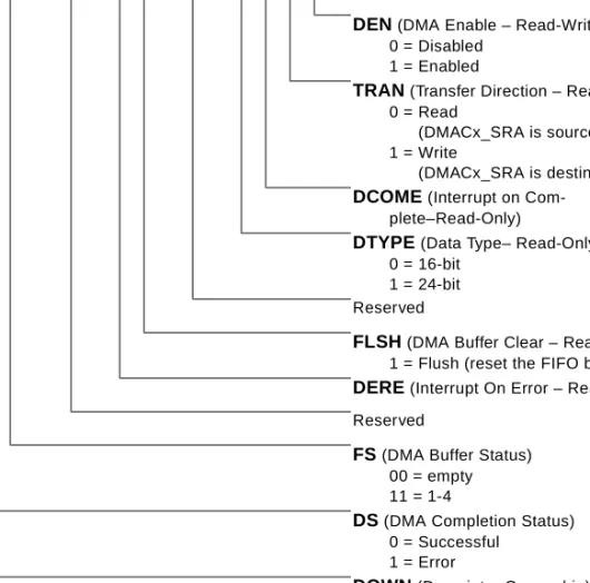
The register address is 0x02:0x101. The DMACW_CFG register should only be written when starting DMA operation. Figure B-7 describes this register bits. Additional information on bits (not covered in the Figure B-7) include:
• Direction: Bit 1 (TRAN) must be set (=1) for the Write operation
• DMA Buffer Clear: Bit 7 (FLSH) should be set (=1) only if a DMA transfer has completed unsuccessfully.
• Descriptor Ownership: Bit 15 (DOWN) is checked before a full descriptor block download is begun to determine if the descriptor
For more information on using DMA processes, see “I/O Processor” on page 6-1.
15 14 13 12 11 10 9 8 7 6 5 4 3 2 1 0
0 0 0 0 0 0 0 0 0 0 0 0 0 0 0 0 Reset = 0x0000
DEN (DMA Enable – Read-Write) 0 = Disabled
1 = Enabled
TRAN (Transfer Direction – Read-Only) 0 = Read
(DMACx_SRA is source) 1 = Write
(DMACx_SRA is destination) DCOME (Interrupt on Com-
plete–Read-Only)
DTYPE (Data Type– Read-Only) 0 = 16-bit
1 = 24-bit Reserved
FLSH (DMA Buffer Clear – Read-Write) 1 = Flush (reset the FIFO buffer) DERE (Interrupt On Error – Read-Only) Reserved
FS (DMA Buffer Status) 00 = empty 11 = 1-4
DS (DMA Completion Status) 0 = Successful
1 = Error
DOWN (Descriptor Ownership) 0 = DSP
1 = DMA
Figure B-7. DMA, MemDMA Channel Write Configuration (DMACW_CFG) Register Bits
DMA Controller Registers
DMA, MemDMA Channel Write Start Page (DMACW_SRP) Reg- ister
The register address is 0x02:0x102. The 16-bit DMA Write Start Page reg- ister holds a running pointer to the DMA address that is being accessed and the memory space being used for a Write transfer. The reset value is
0x0000.
DMA, MemDMA Channel Write Start Address (DMACW_SRA) Register
The register address is 0x02:0x103. This 16-bit read-only register holds the Write transfer start address. The reset value is 0x0000.
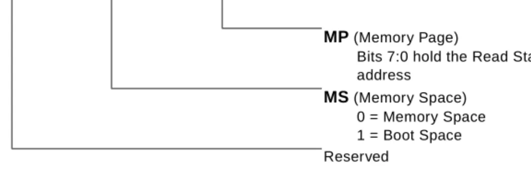
DMA, MemDMA Channel Write Count (DMACW_CNT) Register The register address is 0x02:0x104. The 16-bit Write Count read-only reg- ister holds the number of words in the transfer. The reset value is 0x0000.
15 14 13 12 11 10 9 8 7 6 5 4 3 2 1 0
0 0 0 0 0 0 0 0 0 0 0 0 0 0 0 0 Reset = 0x0000
MP (Memory Page)
Bits 7:0 hold the Write Start Page address
MS (Memory Space) 00 = Memory Space 01 = Boot Space 10 = IO Space 11 = reserved Reserved
Figure B-8. DMA, MemDMA Channel Write Start Page (DMACW_SRP) Register Bits
DMA, MemDMA Channel Write Chain Pointer (DMACW_CP) Register
The register address is 0x02:0x105. The 16-bit DMACW_CP register holds the pointer to address of next descriptor for a Write transfer. The reset value is 0x0000.
DMA, MemDMA Channel Write Chain Pointer Ready (DMACW_CPR) Register
The register address is 0x02:0x106. Bit 0 in the 16-bit Read-Write register sets the status of the descriptor write operation. If bit = 1, the status is Descriptor Ready; 0 = Wait. Bits 15–1 are not used.
This register should be set in the software after each descriptor is written to the internal memory. This lets the DMA know that a new descriptor block has been written in case the state machine has stalled because the descriptor block was not ready. This bit is cleared by the hardware upon beginning the data transfers of the described work block or after a reading a descriptor block with the ownership bit not set. Failure of the software to set this bit could potentially cause the DMA engine to permanently stall waiting for this bit.
DMA, MemDMA Channel Write Interrupt (DMACW_IRQ) Regis- ter
The register address is 0x02:0x107. The DMA, MemDMA Channel can generate an interrupt upon a completion of a transfer. The interrupt occurs after the last write of the transfer is executed. Writing a one to bit 0 of the DMACW_IRQ register clears the DMA interrupt. Bits 15–1 are not used. The reset value is 0x0000. Because this bit is sticky, it needs to be cleared in the interrupt service routine to prevent the interrupt from occurring repeatedly.
DMA Controller Registers
DMA, MemDMA Channel Read Pointer (DMACR_PTR) Register The register address is 0x02:0x180. This is a Read-Only register that holds the pointer to the current descriptor block for the DMA Read operation.
The reset value is 0x0000.
DMA, MemDMA Channel Read Configuration (DMACR_CFG) Register
The register address is 0x02:0x181. The DMACR_CFG register should only be written when starting DMA operation. The reset value is 0x0000. The first descriptor’s address should be written to the DMACR_CP Chain Pointer reg- ister followed by writing a “1” to the configuration register setting the DEN (DMA Enable) bit 0. This will enable the DMA process and the first descriptor block will be fetched from internal memory. The dynamic allo- cation of descriptors is controlled by the “ownership” bit (bit 15) of each descriptor block.
Bit 1 (Direction) is set to 0 for the Read operation.
The DMA, MemDMA Channel generates an interrupt if the “Interrupt on Error” bit 8 is set and the corresponding DMA channel is disabled dur- ing operation. For bit descriptions for this register (which are the same as the DMACW_CFG register), see Figure B-7 on page B-25.
DMA, MemDMA Channel Read Start Page (DMACR_SRP) Reg- ister
The register address is 0x02:0x182. The 16-bit DMA Read Start Page reg- ister holds a running pointer to the DMA address that is being accessed and the memory space being used for a Read operation.
DMA, MemDMA Channel Read Start Address (DMACR_SRA) Register
The register address is 0x02:0x183. This 16-bit read-only register holds the Read transfer start address. The reset value is 0x0000.
DMA, MemDMA Channel Read Count (DMACR_CNT) Register The register address is 0x02:0x184. The 16-bit Read Count read-only reg- ister holds the number of words in the transfer. The reset value is 0x0000.
15 14 13 12 11 10 9 8 7 6 5 4 3 2 1 0
0 0 0 0 0 0 0 0 0 0 0 0 0 0 0 0 Reset = 0x0000
MP (Memory Page)
Bits 7:0 hold the Read Start Page address
MS (Memory Space) 0 = Memory Space 1 = Boot Space Reserved
Figure B-9. DMA, MemDMA Channel Read Start Page (DMACR_SRP) Register Bits
DMA Controller Registers
DMA, MemDMA Channel Read Chain Pointer (DMACR_CP) Register
The register address is 0x02:0x185. The 16-bit DMACR_CP register holds the pointer to the address of the next descriptor for a Read transfer. The reset value is 0x0000.
DMA, MemDMA Channel Read Chain Pointer Ready (DMACR_CPR) Register
The register address is 0x02:0x186. Bit 0 in the 16-bit Read-Write regis- ter sets the status of the descriptor write operation. If bit = 1, the status is Descriptor Ready; 0 = Wait. Bits 15–1 are not used.
This register should be set in the software after each descriptor is written to the internal memory. This lets the DMA know that a new descriptor block has been written in case the state machine has stalled because the descriptor block was not ready. This bit is cleared by the hardware upon beginning the data transfers of the described work block or after a reading a descriptor block with the ownership bit not set. Failure of the software to set this bit could potentially cause the DMA engine to permanently stall waiting for this bit. The reset value is 0x0000.
DMA, MemDMA Channel Read Interrupt (DMACR_IRQ) Regis- ter
The register address is 0x02:0x187. The DMA, MemDMA Channel can generate an interrupt upon a completion of a transfer. The interrupt occurs after the last write of the transfer is executed. Writing a one to bit 0 of the DMACR_IRQ register clears the DMA interrupt. Bits 15–1 are not used.