G E N E R AT I O N O F S PAT I A L L I G H T D I S T R I B U T I O N S
P h D d i s s e r t a t i o n
L Á S Z L Ó D O M J Á N
T U T O R : D R . L Á S Z L Ó K O C S Á N Y I D O C E N T
D e p a r t m e n t o f A t o m i c P h y s i c s F a c u l t y o f N a t u r a l S c i e n c e s
T U B u d a p e s t
2 0 0 4
Ta b l e o f c o n t e n t s
1 Acknowledgements ...4
2 Theses ...5
2.1 Introduction ...5
2.2 Stripe illuminator based on LED array and parabolic mirror for active triangulation sensors used on mobile robots...5
2.2.1 Description of the problem ... 5
2.2.2 The construction and properties of the stripe illuminator ... 6
2.2.3 Summary of new results in technical sciences ... 7
2.3 Theoretical and numerical examination of the stripe illuminator made of a linear emitter placed at the focal line of a cylindrical lens to optimise the operation in external space...8
2.3.1 Description of the problem ... 8
2.3.2 Examination of the stripe illuminator made of a linear emitter placed at the focal line of a cylindrical lens regarding operation in external space ... 8
2.3.3 Summary of new results in technical sciences ... 9
2.4 Ternary phase-amplitude (+1,-1,0) modulation with transmission type twisted nematic liquid crystal displays for smoothing of spatial intensity distribution of Fourier holograms ...10
2.4.1 Description of the problem ... 10
2.4.2 Realisation of ternary phase-amplitude (+1,-1,0) modulation with transmission type twisted nematic liquid crystal displays ... 11
2.4.3 Summary of new results in technical sciences ... 12
2.5 Publications ...13
2.5.1 Publications related to the theses ... 13
2.5.2 Publications in optical engineering and science... 14
3 General introduction ... 15
4 Stripe illuminator based on LED array and parabolic mirror for active triangulation sensors used on mobile robots ... 18
4.1 Introduction ...18
4.1.1 General considerations... 18
4.1.2 Stripe illuminators with lasers... 19
4.1.3 Stripe illuminators with spectral lamps... 20
4.1.4 Stripe illuminators with LEDs ... 21
4.2 Operation principle ...22
4.3 Design process by using an optical CAD software...23
4.3.1 The geometrical optical model of the LED ... 24
4.3.2 The calculation of the optimal parabolic shape and aperture ... 26
4.3.3 Tolerance analysis... 28
4.4 Realisation ...30
4.5 Results and conclusions...31
4.5.1 Optical and geometrical characteristics... 31
4.5.2 Eye Safety ... 34
4.5.3 Results on a mobile robot... 42
5 SNR analysis of the stripe illuminator based on linear emitter and cylindrical lens against solar irradiance ...43
5.1 Introduction ...43
5.2 The radiometric analysis of the stripe illuminator ...45
5.2.1 Definition of source parameters ... 45
5.2.2 Radiance distribution at the exit aperture of the cylindrical lens ... 46
5.2.3 Calculation of the irradiance behind the lens ... 50
5.2.4 Lens parameters yielding maximal total light power ... 53
5.3 SNR against sunshine for sources with different types of emitters ...53
5.3.1 Definition of SNR ... 54
5.3.2 SNR applying LED array... 55
5.3.3 SNR applying laser diode array ... 57
5.3.4 SNR applying incandescent source... 60
5.4 Conclusions ...63
6 Ternary phase-amplitude modulation with transmission type twisted nematic liquid crystal displays for Fourier holographic data storage ...65
6.1 Introduction ...65
6.2 Derivation of the Jones matrix describing both the polarisation and phase modulation of a transmission type twisted nematic LC cell ...67
6.3 Generation and detection of arbitrary elliptical polarisations ...73
6.4 TPA modulation setup of Jang and Shin ...76
6.5 Ternary Phase-Amplitude modulation applying transmission type twisted nematic LC cell ...77
6.5.1 Ternary phase-amplitude modulation with ī=5.2 ... 77
6.5.2 Ternary phase-amplitude modulation with ī=6 ... 80
6.5.3 Ternary phase-amplitude modulation with ī=6.6 ... 82
6.6 Fourier plane homogenization with test images ...83
6.7 Summary and conclusions ...88
7 Appendix I ...89
7.1 Virtual image of a single LED chip ...91
7.2 The virtual image of the whole LED array ...92
8 Appendix II ...94
9 References... 98
1 A c k n o w l e d g e m e n t s
The number of people supporting my research work is very large so I have no chance to list everyone.
First I would like to thank my tutor Dr. László Kocsányi, associate professor of the Institute of Atomic Physics Technical University Budapest, who has given me professional orientation and personal support since I was a university student. Secondly I would like to thank Dr. Gábor Szarvas, technical director of Optilink Hungary RT for the many valuable technical discussions and lots of support to my research activity. I would like to thank Prof. Dr. Péter Richter, Chairman of the Institute of Atomic Physics Technical University Budapest, for helping me in the formulation of my scientific theses and in the preparation of my articles. There are further people, whom I would like to thank for the lots of professional help to find the results published here: Dr. László Gazdag, Sándor Várkonyi, Dr. Pál Koppa, Dr. EmĘke LĘrincz, Dr. Wendelin Feiten, Dr. Gábor Erdei and the whole staff of the Institute of Atomic Physics and the Optilink Hungary RT. At last I would like to thank my family, my father and mother for the personal support and my brother for correcting the English in my publications and dissertation.
2 T h e s e s
2 . 1 I n t r o d u c t i o n
A spatial light distribution can be characterised by the spatial distributions of the following physical parameters depending on the coherence properties of the light: field vector, intensity, mutual intensity, polarisation, spectral power density, radiance. As my scientific theses concern mainly practical applications I do not consider the different possibilities of mathematical interpretation of spatial light distributions with more details.
Different optical applications require the generation of spatial light distributions of different physical properties. E.g. a very general task of technical optics is the generation of a light spot with very small geometrical size that is applied in many fields as optical data storage, laser surgery, laser material processing, etc. The application of movie and image projection requires spatial modulation of the spectral intensity of light according to the image to be projected. Since in most of the cases the light emitted by the primary sources does not meet the requirements of the applications, hence additional optical elements are needed for the modification of the light radiation. Such an equipment consisting of one ore more primary light emitters and some optical elements for the modification of the properties of the emitted light can be called a light source or a light modulator. A spatial light distribution suiting to the requirement of a specific application can be obviously created on many different ways, which raises the problem of finding the technically and economically optimal solutions. Furthermore the steady development of technology enables to find more and more optimal solutions from time to time.
The first and second groups of theses are related to stripe illuminators for robotic applications, where the spatial modulation of the intensity and spectral intensity of light is required. The third groups of theses are related to spatial light modulation for holographic data storage applications, where the spatial modulation of the complex amplitude of polarised coherent light waves are considered.
2 . 2 S t r i p e i l l u m i n a t o r b a s e d o n L E D a r r a y a n d p a r a b o l i c m i r r o r f o r a c t i v e t r i a n g u l a t i o n s e n s o r s u s e d o n m o b i l e r o b o t s
Closely related publications: 1 and 2 of the list given in point 2.5.
2 . 2 . 1 D e s c r i p t i o n o f t h e p r o b l e m
The light sources illuminating only a stripe of space are called stripe illuminators. An ideal light-stripe is such a spatial light distribution in which the light intensity is constant inside a certain three
dimensional stripe of space and zero outside of it. The most important application area of these light sources are the active triangulation sensors with structured illumination, which are also applied as obstacle recognition sensors of autonomous mobile robots (AMR). The target parameters of the developed stripe illuminator were specified according to the requirements of an obstacle recognition sensor developed for an experimental AMR of Siemens (ROAMER) and they are the following: 2m illumination range; stripe width of 6-8 cm; highest possible light intensity to detect objects with low reflexivity; high spectral intensity and simple capability of temporal modulation yielding high SNR against the background illumination in internal space; eye safety; simple construction for cheap production.
2 . 2 . 2 T h e c o n s t r u c t i o n a n d p r o p e r t i e s o f t h e s t r i p e i l l u m i n a t o r
The above requirements can be fulfilled with a stripe illuminator constructed of a linear array of high power LEDs and a cylindrical parabolic mirror. The linear LED array is placed on the focal line cylindrical parabolic mirror and the LEDs are illuminating in the direction of the central line of the parabolic mirror. The light rays emerging from the LEDs are collimated in one direction by reflecting on the cylindrical parabolic mirror. An additional rectangular aperture placed at the plane of the LED array blocks the “off-axis” rays after reflecting on the mirror. This construction supplies very high total light power and intensity because of the large number of applied high power LEDs. The narrow bandwidth of the light emitted by the LEDs enables the spectral filtering of background illumination by applying an optical band-pass filter matched to the emission of the LEDs in the detecting optics.
The application of cheap elements makes the stripe illuminator economically reasonable too.
I built a geometrical optical model of the selected high power LED (Siemens SFH487P, 880nm central wavelength) in an optical CAD system and designed a configuration (parabolic shape, distance between LEDs and mirror, size of rectangular aperture) optimally realising the above listed requirements. I made the tolerance analysis of the LED mounting that resulted tolerances of 0.2 mm for the positioning and 0.3° for the orientation.
The following simple and economic solution was found to realise the designed light source. The calculated parabolic shape was cut into thin metal plates by a precision laser material processing machine. More such metal plates were fixed side by side in a Al box and a flexible mirror foils was stretched onto the parabolic edges of the metal plates by springs. The accurate positioning and orientation of the LEDs were solved by a special assembling and holding frame.
The technical parameters of the realised stripe illuminator are the following. The stripe width is 75 mm (FWHM) at 2 m distance from the source. The intensity of the stripe are 5.5 mW/cm2, 1.1 mW/cm2, 0.6 mW/cm2 at 0.1m, 1m and 2m distances respectively. The spectral intensity of the source was measured to be 69, 14 and 7.5PW/cm2/nm at 0.1m, 1m and 2m distances respectively.
Comparing these values with spectral intensities measured in internal spaces SNRs between 140 (room illuminated by artificial light) and 7 (room illuminated by strong sunshine) can be obtained
depending on the intensity of the background illumination. The operation of the stripe illuminator was tested in a special active triangulation sensor. In internal space the light source supplied detectable signal even for objects of very small reflectivity, as black objects or objects made of transparent glass.
According to the tests all types of objects except fully transparent or reflective surfaces of optical quality could be detected by the light source in internal space. By increasing the numerical aperture of the detecting optics and the detection time surfaces of optical quality may be also detected by the light source. The optical sensor was mounted onto an AMR to test the operation of the light source. The AMR could fulfil all of its navigation tasks by relying only on the signals of the optical sensor about the obstacles lying in its environment. I analysed the eye safety of the stripe illuminator based on physical principles and valid technical norms. Both analyses resulted that the stripe illuminator is eye safe.
2 . 2 . 3 S u m m a r y o f n e w r e s u l t s i n t e c h n i c a l s c i e n c e s
I. I recognised and justified with numerical calculations that the light source constructed of a cylindrical parabolic mirror, a linear LED array placed at the focal line of the mirror and a transmitting aperture of rectangular shape placed at the plane of the LED array realises a high power, eye safe stripe illuminator by which a stripe of less than 9 cm stripe width is illuminated within a distance range of 0-2m. I prove with test measurements that the intensity and spectral intensity of the light stripe are high enough even for the detection of objects with low reflectivity in internal space thus the stripe illuminator can be effectively applied in obstacle recognition sensors based on active optical triangulation. To reach the stripe width of 9 cm the LEDs should be positioned with 0.2 mm tolerance and the orientated with 0.3°
tolerance, which are technically feasible requirements. These tolerance values were calculated in an optical CAD system based on a geometrical optical model of the LED.
II. I recognised that a technically and economically effective solution of this stripe illuminator is a flexible mirror foil stretched onto metal plates having the required parabolic shape; the accurate positioning of the LEDs can be solved with a special mounting and holding frame.
I prove with test measurements that the realised stripe illuminator supplied 75 mm stripe width (FWHM) within the 0-2 m distance range. As the light source of an optical triangulation sensor the stripe illuminator supplied signals high enough even for detecting objects with very low reflectivity (black objects, glass objects). The SNR against the background illumination varied between 140 and 7 depending on the intensity of background light. I justified with radiometric calculations and measurements prescribed by the valid standards that stripe illuminator is eye safe.
2 . 3 T h e o r e t i c a l a n d n u m e r i c a l e x a m i n a t i o n o f t h e s t r i p e i l l u m i n a t o r m a d e o f a l i n e a r e m i t t e r p l a c e d a t t h e f o c a l l i n e o f a c y l i n d r i c a l l e n s t o o p t i m i s e t h e o p e r a t i o n i n e x t e r n a l s p a c e
Closely related publications: 3 of the list given in point 2.5.
2 . 3 . 1 D e s c r i p t i o n o f t h e p r o b l e m
These theses consider the generation of such spatial light distributions that allow active triangulation sensors to operate in external space. The most important noise source for the external operation of these sensors is the intense background light caused by sunshine. The most important condition of efficient operation in external space is that spectral intensity of the stripe illumination should be high enough compared to the spectral intensity of terrestrial solar illumination, consequently the spatial modulation of spectral intensity is required.
2 . 3 . 2 E x a m i n a t i o n o f t h e s t r i p e i l l u m i n a t o r m a d e o f a l i n e a r e m i t t e r p l a c e d a t t h e f o c a l l i n e o f a c y l i n d r i c a l l e n s r e g a r d i n g o p e r a t i o n i n e x t e r n a l s p a c e
I examined in which way stripe illuminators supplying high enough SNRs against solar illumination can be realised by the construction of a cylindrical lens and a linear emitter (in reality rectangular, but one edge is much shorter than the other one) placed at the focal line of the lens. This construction is very effective for realising high power stripe illumination because of the large surface size of the rectangular emitter. Such a light source can be constructed of many different emitter types as LED array, laser diode array and incandescent source, each of them have different physical sizes and angular emission characteristics. My main aim was to set up a general theoretical model by which the illumination of the different practical stripe illuminators can be described, their external space operation can be optimised and the different practical configurations can be compared. Firstly I built a radiometric model of the optical system assuming a spatially invariant rectangular emitter of arbitrary angular radiation distribution and an ideal cylindrical lens. The model resulted an integral by which the (spectral) intensity can be calculated in any point of the illuminated stripe. I determined the optimal focal length and numerical aperture of the cylindrical lens that couples the maximal light power into a stripe of given width from a rectangular emitter of a given geometrical size. By the numerical evaluation of the radiometric integral I examined the SNRs against solar illumination
applying different practical rectangular emitters as linear LED chip array, linear array of packaged LEDs, laser diode array and tungsten incandescent sources. Stripe illuminators with four different geometrical parameters (see Table) were examined by the emitter types listed above.
Configuration Illuminating distance
Stripe width
1 1 m 0.01 m
2 1 m 0.05 m
3 2 m 0.01 m
4 2 m 0.05 m
The SNR was defined as ratio of the spectral intensity of the stripe at maximal distance and the spectral intensity of direct solar radiation. The terrestrial solar spectrum published by the American Society for Testing and Materials were applied in the calculations.
By applying a linear emitter made of linear LED chip array SNRs over one were obtained with chips emitting at 450nm, 660nm and 950nm central wavelengths for all the configurations of the table. The 880nm LED chip array supplied SNR over one for the configurations 1,2 and 4. By applying a linear array of 950nm packaged LEDs SNRs over one were obtained for all the configurations except the 3rd one. SNR over one was obtained also by applying 660nm packaged LEDs for configuration 2. By applying a linear array of 5mW packaged laser diodes SNRs over 0.7 were obtained for all configurations at all the investigated wavelengths (405, 635, 785, 840, 950 and 1550nm). The 405 and 950nm laser diodes supplied SNRs over one for all the configurations. By increasing the power of the laser diodes the SNRs can be further increased. The SNRs were calculated also for tungsten linear sources of 2500K and 3000K temperatures. SNR over one were obtained for the 2nd configuration of the table at wavelengths over 800nm with the 2500K tungsten source and over 540nm with the 3000K one. These sources can be effectively applied if a stripe illuminator with very high total power and broad spectral band is required. For the configurations 1,3,4 the SNR was over one only in very narrow spectral bands (in the solar minima), thus the application of these sources is not advantageous because of the low power efficiency.
2 . 3 . 3 S u m m a r y o f n e w r e s u l t s i n t e c h n i c a l s c i e n c e s
I. I examined and modelled the stripe illuminator made of an ideal cylindrical lens and a spatially invariant rectangular emitter of arbitrary angular radiation distribution placed at the focal line of the lens to examine its effectiveness in external space measurements. I established a radiometric integral by which the (spectral) intensity of the illuminated stripe can be calculated for rectangular emitters of arbitrary angular radiation distribution and an ideal cylindrical lens of arbitrary focal length and aperture size. This model is able to
describe practical stripe illuminators realised with different rectangular sources as LED array, laser diode array and incandescent source.
II. I defined the SNR as the ratio of the spectral intensities of the stripe illuminator and of direct sunshine. By the numerical evaluation of the radiometric integral I calculated the obtainable SNRs for stripe illuminators applying LED chip arrays, arrays of packaged LEDs and laser diode arrays operating at various wavelengths; I also calculated the SNRs using 2500K and 3000K tungsten rectangular sources. According to the obtained SNRs I selected those emitter types by which SNRs over one could be obtained: LED chip arrays of 470, 525, 660, 880, 940 and 950nm wavelengths; packaged LED arrays of 660 and 950 nm wavelengths (very simple and economical solutions!); array of packaged 5mW laser diodes of 405, 635, 785, 840, 950, 1050nm wavelengths; 2500K and 3000K tungsten incandescent sources in different spectral bands defined by the geometry of the illuminated stripe. By these calculations I showed that the stripe illuminator based on a cylindrical lens and a linear emitter can be effectively applied in external space measurements.
2 . 4 T e r n a r y p h a s e - a m p l i t u d e ( + 1 , - 1 , 0 ) m o d u l a t i o n w i t h t r a n s m i s s i o n t y p e t w i s t e d n e m a t i c l i q u i d c r y s t a l d i s p l a y s f o r s m o o t h i n g o f s p a t i a l i n t e n s i t y d i s t r i b u t i o n o f F o u r i e r h o l o g r a m s
Closely related publications: 4 and 5 of the list given in point 2.5.
Other related publications: 6-12 of the list given in point 2.5.
2 . 4 . 1 D e s c r i p t i o n o f t h e p r o b l e m
These theses concern with the spatial modulation of the complex amplitude of linearly polarised coherent light for holographic data storage. In Fourier holographic data storage data images of several bytes of information are stored in holograms. The data images are usually created by spatial light modulators (SLM), the Fourier transformation is made by an objective. A basic problem of Fourier holography is that intensity of the zero spatial frequency component can be several magnitudes higher than the average intensity of other frequencies. Storing such a hologram does not optimally utilise the dynamic range of the storing material. A well known method to destruct the zero frequency component is to give random phase modulations to the different SLM pixels. The conventional solution for this method is that the SLM is imaged onto a random phase mask with same pixel number and geometry as the SLM by an objective of sub-pixel distortion. Both the design and fabrication of an objective with sub-pixel distortion and the 6 axes alignment required for the pixel matched positioning of the SLM and phase mask are complicated technical tasks, thus this is a very
uneconomical solution. Furthermore for those data images in which the bright SLM pixels well correlate with the phase mask pixels of similar phase shifts the zero frequency component is not destructed, thus they should be prevented by coding techniques that leads to data capacity losses.
Because of the above described reasons it would be very advantageous to realise the spatial amplitude and phase modulation of light required for the generation of Fourier holograms with smoothed intensity distributions with a single SLM pixel.
2 . 4 . 2 R e a l i s a t i o n o f t e r n a r y p h a s e - a m p l i t u d e ( + 1 , - 1 , 0 ) m o d u l a t i o n w i t h t r a n s m i s s i o n t y p e t w i s t e d n e m a t i c l i q u i d c r y s t a l d i s p l a y s
My research work concerned with the problem of realising the required complex amplitude modulation of light by applying a single pixel of a transmissive twisted nematic LCD. The simplest answer for the described problem is the ternary phase-amplitude (TPA) modulation containing three states with complex amplitude modulations of +1,-1 and 0. This modulation scheme is already known in the field of correlation filters.
The complex amplitude modulation of an ideal transmission type twisted nematic LC cell can be described by a Jones matrix assuming that the LC molecules are uniformly twisting within the LC medium. According to the model the LC cell has two important parameters: the phase retardation that can be modulated between a maximal value and zero by applying electrical field to the cell, the maximal value is taken at zero field; and the twist angle of the LC molecules within the cell that is invariant to the applied electrical field and approximately equal to r90° for commercially available LCDs. The elements of Jones matrix are non-linear functions of the phase retardation and the twist angle. In order to obtain TPA modulation I placed the LC cell between an “elliptical polariser” and an
“elliptical analyser”. Based on the Jones matrix I built a numerical model by which the complex amplitude modulation of the LC cell could be evaluated for arbitrary elliptically polarised illumination and light detection. An elliptical polarisation can be described by two independent parameters (e.g.
ratio of major and minor axes and direction of major axis) thus the illuminated and detected elliptical polarisations can be described by four independent parameters. The complex amplitude modulation of the LC cell was calculated as a function of the phase retardation in points of the four dimensional parameter-space that describes the incident and detected elliptical polarisations. The elliptical
A n e l l i p t i c a l p o l a r i s e r i s a n o p t i c a l e l e m e n t u s e d t o g e n e r a t e a r b i t r a r y e l l i p t i c a l p o l a r i s a t i o n . O n e r e a l i s a t i o n i s a s e q u e n c e o f a r e v o l v i n g l i n e a r p o l a r i s e r a n d a r e v o l v i n g q u a r t e r w a v e p l a t e . A n e l l i p t i c a l a n a l i s e r i s c a p a b l e o f t r a n s m i t t i n g o n e e l l i p t i c a l p o l a r i s a t i o n a n d b l o c k i n g t h e o r t h o g o n a l e l l i p t i c a l p o l a r i s a t i o n . I t c a n b e r e a l i s e d b y t h e s e q u e n c e o f a r e v o l v i n g q u a r t e r w a v e p l a t e a n d a r e v o l v i n g l i n e a r p o l a r i s e r .
polarisations for which the LC cell realises TPA modulation were found by computer search. The searching condition was that the calculated complex amplitude modulation function must contain three points of complex amplitudes A1,A2,H with the following conditions: 0.95<|A1/A2|<1.05;
0.95S<arg(A1/A2)<1.05S; |A1|2/|H|2>15. As the maximal phase retardation of an LC cell depends on the wavelength and different LCDs have different maximal phase retardations as well, hence the computer search was executed for more different maximal phase retardation values. By increasing the maximal phase retardation better modulation capabilities are expected. Applying an LC cell with 5.2 phase retardation TPA modulation can be obtained with an amplitude transmission of |A1|||A2|=0.5, namely 25% of the incident light power can be utilised. An LC cell with a phase retardation of 6 supplies TPA modulation with |A1|||A2|=0.6, thus 36% of the light power is utilised. An LC cell with a phase retardation of 6.6 yields TPA modulation with |A1|||A2|=0.9, thus 81% of the light power is utilised. In the last case |H|=0.16 resulting a contrast ratio of (0.9/0.16)2=32 between the intensities of the bright and dark states. The intensity contrast ratios in the first two cases were 15 and 16.
I made test measurement to verify the calculated results experimentally applying a transmission type twisted nematic LCD of Sony (LCX017DLT). The TPA modulation characteristics calculated for phase retardations of 5.2 and 6 were measured at 532 and 473 nm wavelengths respectively. The measured complex modulation curves were consistent with the calculations, TPA modulation could be experimentally realised with similar parameters as the calculations predicted. The intensity of the Fourier plane were compared for TPA and normal intensity modulation of 2 states applying test data bit patterns. Applying conventional intensity modulation of 2 states the ratio of peak and average intensities of the Fourier plane was 200:1, while in the case of TPA modulation it was 8:1.
2 . 4 . 3 S u m m a r y o f n e w r e s u l t s i n t e c h n i c a l s c i e n c e s
I. I recognised that TPA modulation can be realised with transmission type twisted nematic LC cells of approximately r90° twist angle, if the LC cell is placed between an elliptical polariser and an elliptical analyser and the configurations of the elliptical polariser and analyser are optimised to the phase retardation of the LC cell.
II. I recognised that by increasing the phase retardation of the LC cell and applying an elliptical polariser and analyser optimised to the increased phase retardation the properties of TPA modulation (transmission of bright states, contrast ratio between intensities of bright and dark states) can be enhanced. I showed with numerical calculations and test measurements that with phase retardations of 5.2, 6 and 6.6 the obtainable amplitude transmissions of TPA modulation are 0.5, 0.6 and 0.9 respectively. The contrast ratios between the intensities of bright and dark states are 15,16 and 32 respectively for the above phase retardation values.
2 . 5 P u b l i c a t i o n s
2 . 5 . 1 P u b l i c a t i o n s r e l a t e d t o t h e t h e s e s
1. Domján L, Kocsányi L, Richter P, Várkonyi S, Feiten W. Stripe illuminator based on LED array and parabolic mirror for active triangulation sensors used on mobile robots. Optical Engineering;
2000, 39(11): 2867-2875
2. Domján L, Kocsányi L, Richter P, Szarvas G, Várkonyi S, Feiten W. Optisches Sensorsystem zur Detektion eines Objektes. German Patent; 1999, 19810366.9, International patent pending
3. Domján L, Kocsányi L, Richter P, Jeszenszky É.: SNR analysis of the stripe illuminator based on linear emitter and cylindrical lens against solar irradiance. Optics and Lasers in Engineering, 2003, 40(3), p. 201
4. Domján L, Koppa P, Szarvas G, Reményi J. Ternary phase-amplitude modulation with twisted nematic liquid crystal displays for Fourier-plane light homogenization in holographic data storage.
Optik, 2002, 113(9), p. 382
5. Reményi J, Várhegyi P, Domján L, Koppa P, E LĘrincz: Amplitude, phase and hybird ternary modulation modes of a twisted-nematic liquid crystal display at 400 nm. Applied Optics (accepted in 2003)
6. Reményi J, Koppa P, Domján L, LĘrincz E.: Phase modulation configuration of a liquid crystal display, presented at the 19thCongress of the International Comission of Optics, Florence, Italy, 25-31 August 2002
7. Szarvas G, Domján L, Koppa P, Erdei G, SütĘA: Capacity estimation for thin film multilayer holographic storage with confocal filtering, Proceedings of the EOS Topical Meeting on Advanced Imgaing Techniques, 20-23 October 2003, Delft, The Netherlands
8. Szarvas G, Koppa P, Erdei G, Domján L, SütĘ A: TöbbrétegĦ, nagy adatsĦrĦségĦ, térfogati mikro- holografikus adattárolási eljárás és rendszer, Hungarian patent application, 15 May 2003, P0301354 / 4, International patent pending
9. Domján L, Erdei G, Koppa P, Szarvas G, Ujvári T, Method and apparatus for encrypting and authenticating of data using phase-coded holographic storage, Hungarian patent application, P0104147, 2001, International patent pending
10. Domján L, Erdei G, Koppa P, Szarvas G, Ujvári T, Method and apparatus for the encryption of data Hungarian patent application, P0104183, 2001, International patent pending
11. Koppa, Várhegyi, Újvári, Lovász, Szarvas, Ujhelyi, Erdei, Reményi, Domján, SütĘ, Lorincz:
Holographic data storage in thin polymer films, Proceedings of SPIE -- Volume 5216, p. 165
12. Szarvas G, LĘrincz E, Richter P, Koppa P, Erdei G, Fodor J, Kalló P, SütĘ A, Domján L, Újhelyi F: Method and apparatus for the distribution of data marks on a medium, and method and apparatus for the holographic recording and readout of data, Hungarian patent, February 4 2000, P 0000518, International patent pending
2 . 5 . 2 P u b l i c a t i o n s i n o p t i c a l e n g i n e e r i n g a n d s c i e n c e
13. Domján L, Szarvas G, Mike Sz: Binokuláris videó szemüveg optikai rendszere, Hungarian patent application, 21 November 2002, P020399314. Domján L, Szarvas G, Mike Sz: Optical arrangements for head-mounted displays, US patent application, 18 November 2003,
15. Domján L, Szarvas G, Mike Sz: Multiple imaging arrangements for head-mounted displays, US patent application, 18 November 2003,
3 G e n e r a l i n t r o d u c t i o n
Optical devices are very widely used in consumer products and in industrial and scientific applications as well. The most important consumer product areas based on optical technologies are lighting products (e.g. room or car lamps), data storage devices (CD,DVD,MO), communication systems, photographic and video systems and eye correction glasses. I can list only some of the industrial applications since there are very many of them: microscopes, machine controlled inspection systems, laser material processing, lithographic systems, position measurements applied in e.g. geodesy and robotic applications. Optical systems are also utilised in various fields of nature science as biology, medicine, astronomy, chemistry, material and environmental sciences, etc.
My PhD thesis relate to the establishment of spatial light distributions optimised to meet the requirements of special applications. A device that creates a certain spatial light distribution can be called a light source or a light modulator. Such a device contains usually at least one light emitter and some optical elements (lenses, mirrors, filters, polarizers, etc ) that modify the illumination to meet the requirements of the special optical applications. Some examples of applications requiring special spatial light distributions are: spatial modulation of light intensity is required in film and image projection applications; the focusing of light into a very small spot is a general problem in many applications as data storage, laser surgery, laser material processing; the establishment of spatial light structures as stripes, gratings, circular patterns is required in position sensing using structured illumination. Such spatial light distributions can be usually created on many ways because of the wide variety of light emitters (e.g. lasers, LEDs, gas lamps, incandescent sources) and light modulating tools. Hence finding an optimal solution regarding technological and economical objectives is a non trivial issue. Furthermore the technological progress in the fields of light emitters, light modulating elements, modelling tools and computer technology enables to find more optimal solutions from time to time for a given application.
Chapters 4 and 5 deal with the establishment of stripe illuminators for robotic applications. Robot manipulators are already applied in many fields of industrial systems as e.g. mounting, painting, drilling, food production. Another very interesting field of robotics are the autonomous mobile robots (AMR) which are very intensively researched both in university and industrial laboratories. A typical AMR is a vehicle capable of moving autonomously within an environment that is either partially known or absolutely unknown by it. Such AMRs can be applied both in industrial and consumer applications as cleaning robots, transport robots, agriculture robots, etc. In order to make accurate and safe movements without hitting the humans and the objects surrounding the robot sensors are required to recognise the objects and to measure their positions. There are many different types of AMRs developed by universities and industrial research laboratories such as the ROAMER of Siemens and the human like robots of Honda, which are not yet widely applied in industrial or consumer applications. From pure technical point of view today’s AMRs are capable of solving different tasks
without threatening the health or material property of human beings, but the high costs of the reliable and accurate sensors prevent the widespread application of this technology both in the consumer and the industrial areas. Hence huge efforts are made to develop low cost sensors for reliable obstacle recognition and position measurement. Chapter 4 of my dissertation discusses a low cost stripe illuminator designed for active vision systems applied in AMRs. The stripe illuminator is based on a cylindrical parabolic mirror and a linear LED array placed at the focal line of the mirror. The stripe illuminator effectively worked on the AMR of Siemens (ROAMER) as part of a low cost stripe illumination based active vision sensor system. The design of this stripe illuminator concentrated mainly on two parameters: on the irradiance and spectral irradiance of the light stripe. High irradiance was required to detect objects with low reflectivity and high spectral irradiance was needed to achieve good signal to noise ratio (SNR) against the background illumination. The achieved spectral irradiance was high enough to obtain excellent SNRs against the background illumination of indoor environments, but in outdoor environment with direct sunshine the source could not be applied.
Chapter 5 consider stripe illuminators based on a cylindrical lens and a rectangular emitter placed at the focal line for outdoor applications. The examination focuses on the spectral irradiances of the stripe illuminators realised with different rectangular emitters such as LED array, laser diode array and incandescent sources of different temperatures. By comparing the obtained spectral irradiances with the spectral irradiance of direct sunshine the achiveable SNRs against sunshine are calculated.
The spectral irradiances and the SNRs are calculated by applying the means of radiometry and the theoretical radiation characteristics of the analysed emitter types.
Chapter 6 deals with establishing special spatial light distribution for holographic data storage in which the complex amplitude of light is spatially modulated. In holographic data storage the storage unit is a hologram that can store a data image containing up to megabits of data, in contrast to conventional digital optical data storage (CD,DVD) in which the storage unit is a single spot storing usually only a single bit of information. The storage holograms can be written side by side in a single thin layer or can be written on a multiplexed way into volume of holographic storing material as well.
The main advantage of holographic storage over the conventional digital optical storage techniques is that extremely high storage capacity can be obtained through volume multiplexing of holograms.
According to theoretical calculations and experimental data e.g. in a multiplexed holographic disk having the same geometrical measures as a compact disk more than one terabytes of information can be stored. It is well known that similar or even higher amounts of data can be stored by semiconductor memories and magnetic hard drives as well. The main advantage of holographic and in general of optical disks over these concurrent technologies is that the cost of the storing medium is significantly lower. An other advantageous application area of this technology is high security data storage. By applying a spatially phase modulated reference beam during hologram recording a physical encryption of the stored data can be achieved. The data image stored in the hologram can be read only if the hologram is illuminated with the same phase modulated reference beam used at recording, thus the data specifying the phase modulation of the reference beam make an encryption key. Holographic data
storage has been intensively researched for 20-30 years but today there is no commercial product based on this technology. The lack of products is mainly caused by the expensive elements required in a holographic storage device such as coherent laser, spatial light modulator, CCD sensor and objectives corrected for wide object field. Hence technological improvements reducing the costs are essentially needed by holographic data storage to leave the laboratory. The data image stored in a hologram is displayed by a spatial light modulator (SLM) which is illuminated with a coherent light beam. In thin storing material the Fourier transform of the data image is usually stored to achieve optimal data density. In order to get rid of the high peak at zero frequency of the hologram the data image should be both amplitude and phase modulated. Conventional SLMs are optimised for modulating only the intensity of light to display images for the eye or a camera. The phase modulation is usually obtained by an external phase modulating mask having the same pixel number and geometry as the SLM and the two devices are imaged onto each other with sub-pixel resolution. Both an objective supplying sub-pixel distortion and the six axes alignment of the SLM and phase mask are expensive technologies. Chapter 6 considers the realisation of the required amplitude any phase modulation of light by applying a single twisted nematic liquid crystal SLM of transmission type, which is the most conventional SLM available on the market. By illuminating the SLM with elliptically polarized light and detecting elliptical polarization the required amplitude and phase modulation of light can be achieved. Since each SLM pixels can be operated independently the complex amplitude of light can be spatially modulated.
4 S t r i p e i l l u m i n a t o r b a s e d o n L E D a r r a y a n d p a r a b o l i c m i r r o r f o r a c t i v e t r i a n g u l a t i o n s e n s o r s u s e d o n m o b i l e r o b o t s
4 . 1 I n t r o d u c t i o n
4 . 1 . 1 G e n e r a l c o n s i d e r a t i o n s
Stripe lighting sensors are widely used in robotics to measure the position of obstacles in the workspace of an autonomous mobile robot [1.][2.][3.]. They operate on the principle of illuminating a light stripe ( usually horizontal) around the robot (see 4.1. Fig.), and this room area is surveyed by a camera. If an obstacle is hit by the light stripe, it scatters a portion of the illumination back, which causes a bright-spot in the image of the detecting camera. Through determining the position of the image spot by image processing, the position of the obstacle can be calculated, if we know the relationship between the image points and the points of the light stripe. The camera lens transforms the points of the room onto the 2 dimensional imaging device. Knowing the parameters of this transformation is neccesary to make position measurements with a stripe lighting sensor.
M obile robot
Video c am era View ing area
Stripe illum inat ion
B a s i c s t r i p e - l i g h t i n g s e n s o r s e t u p u s e d o n a m o b i l e r o b o t 4 . 1 . F i g .
In this paper we want to focus on the problem of finding an efficient and economic stripe illuminator for the above purpose.
The three main characteristics of a stripe illuminator are:
1. The irradiance of the illuminated light (measured in mW/cm2).
2. The spectral irradiance of the illuminated light (measured in mW/cm2/nm).
3. The geometrical width of the stripe.
We discuss first the influence of the irradiance. The detectability of objects with low reflectivity becomes better by increasing the irradiance. If the source is to be used on a mobile robot, which operates among people, it is a further requirement that the source must not injure the human eye. This limits the irradiance of the illuminated light depending on the wavelength and on the type of the source.
High spectral irradiance helps supressing the disturbing effects of the background light. The background light in the environment of the robot is the main noise-source for a striping sensor [1.].
There are two possibilities for suppressing the effects of the disturbing background illumination. If the stripe illuminator emits just in a narrow spectral band (such as lasers and LEDs), then by using an optical bandpass filter which is fitted to the spectral band of the light source in front of the camera the background light can be supressed. Another filtering method can be used when the light source is pulsed, and two images, one with and one without stripe illumination are taken. By substracting the second image from the first, the signals originating from the background illumination cancel. If it is neccesary, both methods can be used simultaneously.
The width of the light stripe influences the achiveable distance resolution of the sensor. The less the stripe width is, the better the achiveable resolution becomes. Namely the localization of an object is based on the fact that it has to be on the intersection of the illuminated stripe and of the line, drawn from the corresponding image point through the center of the camera objective. By decreasing the width of the light-stripe, this intersection becomes shorter, therefore the resolution becomes better.
However decreasing the stripe width has also a drawback, namely that the space covered by a light- stripe becomes narrower, and the number of stripe illuminators needed to cover the whole room increases.
4 . 1 . 2 S t r i p e i l l u m i n a t o r s w i t h l a s e r s
Laser
Collimating lens
Cylindrical lens
Light stripe
S t r i p e - i l l u m i n a t o r w i t h l a s e r a n d c y l i n d e r - l e n s 4 . 2 . F i g .
The most widely used version for a stripe illuminator is a collimated laser and a cylindrical lens, where the cylindrical lens creates the needed light stripe (see 4.2. Fig.). The main advantages of this version are that the stripe width can vary between small (1mm) and large (10cm) values, and that the very small spectral bandwidth of lasers enables a very high spectral irradiance. In addition the electronic pulse modulation of semiconductor lasers is easy and finally, that the optics used is quite simple. The main drawbacks are: the high costs of lasers, and the very strict eye safety limits for laser sources [4.][13.], which may limit the application in a strongly illuminated environment.
4 . 1 . 3 S t r i p e i l l u m i n a t o r s w i t h s p e c t r a l l a m p s
Cylindrical lens
Spectral
lamp Light stripe
Spectral lamp
Collimating Light stripe lens
Light stripe Conic
mirror
S t r i p e i l l u m i n a t o r v a r i a t i o n s w i t h s p e c t r a l l a m p s 4 . 3 . F i g .
Stripe illuminators can also be produced with different types of spectral lamps (e.g. gas lamps, incandescent lamps). Two common arrangements for creating light stripes with spectral lamps are shown in 4.3. Fig.. In the first version the stripe is produced by a cylindrical lens [5.]. In the second version the rays are first collimated by a lens and the parallel beam is projected onto a conic mirror having an axis parallel with the beam. The conic mirror reflects the rays in such a way that a light stripe normal to the cone-axis is produced. In order to collect a portion of those rays, which are not emitted in the direction of the lens, sometimes a back reflector used.
The main advantages of the application of spectral lamps in stripe illuminators are, that a very high irradiance, and a good spectral irradiance can be achieved. But it has also disadvantages. Since only a small portion of the total emitted light can be collected and collimated, therefore in order to achive a high spectral irradiance (e.g. 10PW/cm2/nm at 1m distance) a total light power of hundreds of Watts are needed for the whole stripe. The application of such high power lamps on a mobile robot is
inpractical. The simplest solution for periodical pulsing of such lamps at the frequency needed (>10 Hz) is mechanical chopping, which is also disadvantageous compared to electronic modulation.
4 . 1 . 4 S t r i p e i l l u m i n a t o r s w i t h L E D s
Stripe illuminators can also be constructed using LEDs. The rapid progress of LEDs in the last decade enabled them to substitute for incandescent sources in applications, in which high irradiance is needed, as e.g. break-lamps of cars [6.][7.] or lasers in medical therapy[8.]. The main advantage of LEDs over spectral lamps is that the LEDs emit with higher spectral radiances (measured in mW/cm2/sr/nm). The technical parameters of an emitter (radiance, spectral radiance, ability of collimation), which are important when making a stripe illuminator of it, are superior for lasers compared to LEDs. According to [4.] the same eye safety regulations are as valid for LEDs as for lasers, but since the emitting area of LEDs (~0.4x0.4 mm) is much greater than the emitting area of laser diodes (~10x10 µm) LEDs are expected to supply better eye safety. A further advantage of LEDs compared to lasers is their lower costs. This can be very important in mass production, primarily when an array of sources is needed to be used in an application requiring a high total light power (>500mW). Since the power of a single LED (20 mW) or a cheap Laser Diode (10 mW) is not strong enough for a striper sensor used in a well illuminated environment (>1W needed), the application of an array of cheap, high power LEDs is an effective and economical solution.
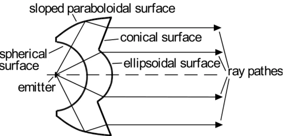
Creating a light-stripe with LEDs is a problem similar to creating a collimated beam, because in most cases using the "cylindrical form" of the collimating optics yields a stripe illumination. Collimation of LED light has been studied by some articles. Wilcken [9.] describes two optical setups for collimating the light of LEDs using conventional optical elements. In the first one an LED with a flat-truncated package is equipped with a pin-hole aperture that makes a semi point light source. The beams leaving the pin-hole are collimated with an objective lens of large Numerical Aperture (Effective Focus Length (EFL)=4.59mm, NA=0.5). In the second one, the beams of an LED with an integrated lens are focused into a pin-hole aperture by an objective lens of the same type, and the beams leaving the aperture are collimated with a second objevtive lens. Both versions give a collimated beam of high quality. The main disadvantage is the high loss of the emitted power (about 90%) because of the pin hole. Spigoulis describes in [10.] a complex optical element, which is proposed for collimating or focusing the light of semi-point sources as e.g. LEDs (see 4.4. Fig.). First the rays of the emitter enter slightly refracted into the element through a spherical surface. Then the rays close to the axis are collimated by refraction on an ellipsoidal surface, and the rays with larger angles are first totally internally reflected on a sloped paraboloidal surface and then refracted on a conical surface.
spherical
conical surface ellipsoidal surface sloped paraboloidal surface
surface emitter
ray pathes
C o m p l e x o p t i c a l e l e m e n t o f S p i g o u l i s f o r c o l l i m a t i n g a n d f o c u s i n g t h e l i g h t o f s e m i - p o i n t s o u r c e s
4 . 4 . F i g .
Parkin and Pelka present a Fresnel-like lens with a lot of facets for collimating or focusing the light of LEDs and lamps [11.]. The rays at different heights are collimated through total internal reflection on different facets of the lens. The advantage of the last two collimators is that they collect the emitted rays in large acceptance angles, so a great portion of the total emitted power is collimated. By using the cylindrical form of any of these systems with a linear LED array on the focal line, a technically effective stripe illuminator could be created, but the production costs of a master, by which such cylindrical optical elements can be produced with complicated, non-circular cross-sections, are very high.
In summary I recognised that none of these solutions leads directly to an efficient, eye-safe and cost effective stripe illuminator.
4 . 2 O p e r a t i o n p r i n c i p l e
My aim was to create a stripe illuminator thatx has a maximal full stripe width of 6-10cm (suitable for a number of robotic applications), x supplies high irradiance,
x supplies high spectral irradiance,
x can be electronically modulated up to 10 Hz frequency.
A stripe illuminator meeting these requirements is shown in 4.5. Fig. It consists of a cylindrical mirror with parabolic cross-section, and of a linear array of high intensity IR LEDs. The focal line of the mirror is the line containing the focal points of all the parabolic cross sections, and the base line is the line containing all their base points. The operating principle is that a parabolic mirror collimates the beams of a point source, if it is located at the focal point. Therefore, if we put an array of point sources onto the focal line of a cylindrical parabolic mirror, then the beams, after reflection on the mirror, will be parallel with the plane, defined by the focal line and the base line. So we get a stripe illumination.
Since the LEDs can not be regarded as point sources, the effect of finite source size needs to be considered. The coordinate system applied in this chapter is shown in 4.5. Fig. The x axis is parallel
with the focal line of the mirror, z is parallel with the axis of the parabolic cross sections, and y is perpendicular to the illuminated stripe. The LEDs are positioned along the focal line of the mirror with an orientation, such that their optical axes are parallel with the z axis.
y x z
Cylindrical parabolic mirror Linear LED array
Light stripe 6-10 cm
T h e b a s i c s t r u c t u r e o f t h e l i g h t s o u r c e 4 . 5 . F i g .
4 . 3 D e s i g n p r o c e s s b y u s i n g a n o p t i c a l C A D s o f t w a r e
I decided to use IR LEDs because they have the maximum light power. High power IR LEDs are available with truncated flat surface or with integrated lens. I chose LEDs with flat surface, because the integrated lens has poor imaging quality, and this makes the LED less point-like. The Siemens SFH 487P LED was selected that has a continuous output light power of 22mW at 880nm central wavelength and a truncated T1 3mm plastic package. In order to evaluate the concept and to find the optimal parabolic geometry, a geometrical-optical model of the whole system in the CAD software OSLO Six was created.4 . 3 . 1 T h e g e o m e t r i c a l o p t i c a l m o d e l o f t h e L E D
PN junction Spherical back reflector
Plastic package
Front surface of chip z
y
Front surface of package
Cylindrical side of package
p side of junction
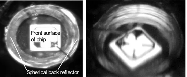
T h e s t r u c t u r e o f t h e S i e m e n s S F H 4 8 7 P L E D w i t h o u t r a y s 4 . 6 . F i g .
The structure of the LED consists of an emitting chip, a metal back reflector of spherical shape, and a plastic package (see 4.6. Fig.). Through consultations with the manufacturer I got to know the exact structure and positioning of the chip and the internal back reflector. This information was necessary to simulate the light generation and extraction in the LED. The simulation model was the following: the light is generated in the pn-junction and propagates in all directions towards the different chip surfaces. The rays that arrive at the first surface with an incident angle less than the angle of total reflection refract at the surface and leave the chip. The rays with an incident angle over the angle of total reflection reflect and propagate towards the next surface of the chip. The rays that reach the substrate are stopped, because the substrate is not transparent to the generated light.
Sides of plastic package
Emitting chip
Back reflector
T h e m o d e l o f t h e S i e m e n s S F H 4 8 7 P L E D w i t h e m i t t e d r a y s
4 . 7 . F i g .
As 4.7. Fig. shows, a portion of the rays leave the chip through the front surface and propagates towards the front surface of the package. An other portion of the rays leaves the chip through the sides of the chip, mainly close to the junction, and propagates to the back reflector, and after reflecting or scattering propagates towards the front surface. 4.8. Fig. shows two camera images of the LED at 100mA forward current. In 4.8. Fig./a a microscope image is shown in which the axes of the LED and of the microscope were parallel. Because of the limited numerical aperture of the microscope 4.8.
Fig./a shows the radiant intensity distribution of the chip and reflector for those rays that propagate close to the optical axis of the LED. As it can be seen in this case the most significant portion of the total emission comes from the front surface of the chip and a much less significant portion comes from the total surface of the back reflector. As the LED illuminates in a wide angular field another microscope image was taken with an arrangement in which the LED was tilted and the optical axes of the microscope and of the LED subtended about 30 degrees (see 4.8. Fig./b). In this image the brightness of the reflector is much closer to the brightness of the chip surface than in the previous image, thus in this tilted direction the reflector illuminates similar radiant intensity as the chip does.
The appearance of these images can be explained quite well by the model. As 4.7. Fig. shows a portion of the rays leave the chip through the front surface, that is why the front surface is bright and sharp in both microscope images. Another portion of the rays leaves the chip at the sides and illuminates the whole area of the back reflector. After reflecting and scattering on it they leave the package mainly in skew directions. The optical model of the LED and two measured microscope images justify that both the chip and the internal reflector of the LED “radiate”, thus both of them should be taken into account when designing light sources with this LED. A good practical estimation is that the total emission of this LED comes from a circular aperture having the same diameter as the aperture of the back reflector (1 mm). It is important to emphasize that this 1 mm aperture diameter is much less than the diameter of the plastic package (3.25 mm) but larger than the lateral size of the chip (0.4*0.4 mm).
Front surface of chip
Spherical back reflector
a: Camera image of SFH 487P LED taken in the direction of LED axis
b : C a m e r a i m a g e o f S F H 4 8 7 P L E D t a k e n i n a n a n g u l a r d e v i a t i o n f r o m t h e L E D a x i s 4 . 8 . F i g .
4 . 3 . 2 T h e c a l c u l a t i o n o f t h e o p t i m a l p a r a b o l i c s h a p e a n d a p e r t u r e
Blocking apertures
LED
Parabolic mirror
Aperture height z
y
35.2
y - z c r o s s s e c t i o n o f t h e s t r i p e i l l u m i n a t o r 4 . 9 . F i g .
The basic setup of our light source consists of an LED, a cylindrical parabolic mirror and a blocking aperture (see 4.9. Fig.). The blocking aperture, which has a rectangular shape, serves to stop the rays propagating "far" from the optical axis and so reduces the width of the stripe. At the same time it reduces the total emitted power by blocking a portion of the emission.
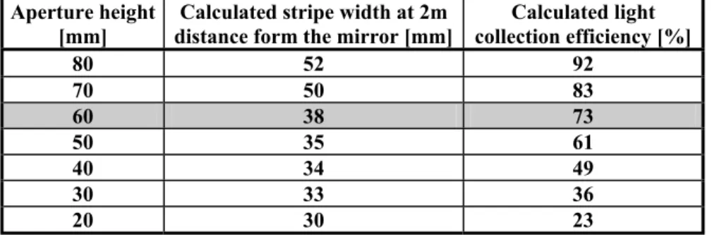
The design evaluation consisted of the following steps: I tested the basic setup with parabolic cross sections of different sizes ( R = 60, 70, 80, 90 mm, parabola equation: y = 1/(2*R)*x2[mm] ) and with different aperture heights (from 20 to 90 mm). I calculated the resulting stripe widths at 2m distance and the ratios of the power collected into the stripe over the total emitted light power. These values were estimated as the ratio of the number of rays transmitted by the aperture relative to the total numbers of rays that arrived at the parabolic mirror. This is an important characteristic for the different setups, because apertures of different heights transmit different percentages of the total radiation. With the parabolas of 60 and 70 mm radii the divergence angle of the illuminated light was too high and this resulted too high stripe widths at reasonable light collection efficiencies. The higher divergence angle of the illumination is caused by the shorter focal lengths of the parabolas of shorter radii. 4.1. Table and 4.2. Table show the calculation results for R = 80 and 90 mm parabolic cross sections, which make the two best candidates for choosing the most effective parabolic shape for the stripe illuminator.
Aperture height [mm]
Calculated stripe width at 2m distance form the mirror [mm]
Calculated light collection efficiency [%]
80 52 92
70 50 83
60 38 73
50 35 61
40 34 49
30 33 36
20 30 23
R e s u l t s o f c a l c u l a t i o n s f o r t h e c y l i n d r i c a l m i r r o r o f p a r a b o l i c c r o s s s e c t i o n d e f i n e d b y y = 1 / ( 2 * 8 0 m m ) * x2 [ m m ]
4 . 1 . T a b l e
Aperture height [mm]
Calculated stripe width at 2m distance form the mirror [mm]
Calculated light collection efficiency [%]
90 56 92
80 52 84
70 45 75
60 37 65
50 34 54
40 31 44
30 29 33
R e s u l t s o f c a l c u l a t i o n s f o r t h e c y l i n d r i c a l m i r r o r o f p a r a b o l i c c r o s s s e c t i o n d e f i n e d b y y = 1 / ( 2 * 9 0 m m ) * x2 [ m m ]
4 . 2 . T a b l e
All the stripe widths shown in 4.1. Table and 4.2. Table are under 60mm, but I supposed that the stripe width of the real source would become bigger because of the misplacements and bad alignments of the LEDs. Therefore the R=80 mm parabolic cross section with 60 cm aperture height (see the highlighted row in 4.1. Table) was selected as an optimal setup for the application. 4.10. Fig. shows the projection of the ray paths in the yz-plane for this setup. According to the calculations in ideal case this setup can supply a light stripe of 4 cm width at 2 m distance that is below the required 6-10 cm. It is worth to mention that the selected cylindrical parabolic mirror has a focal length of 40 mm.
P r o j e c t i o n o f r a y p a t h e s t o t h e y z - p l a n e f o r t h e c y l i n d r i c a l m i r r o r w i t h a p a r a b o l i c c r o s s s e c t i o n , d e s c r i b e d b y y = 1 / ( 2 * 8 0 m m ) * x2 [ m m ] , a n d w i t h 6 0 c m a p e r t u r e h e i g h t
4 . 1 0 . F i g .
4 . 3 . 3 T o l e r a n c e a n a l y s i s
z
x
y
DX DZ DY Cylindrical parabolic
mirror
Linear LED array
D e f i n i t i o n o f m i s p l a c e m e n t p a r a m e t e r s f o r t o l e r a n c e a n a l y s i s 4 . 1 1 . F i g .
All previously described calculations were made with one LED and the LED was in the optimal position and orientation in front of the cylindrical-parabolic mirror. In the realisation a linear array of LEDs is used that are mounted onto a printed circuit stripe. In this case the misplacements of the different LEDs cause an increase of the stripe width. Therefore a tolerance analysis was carried out considering the errors in the position and orientation of the LEDs. The position of any misplaced LED can be expressed with 3 misplacement vectors (DX, DY, DZ). The misplacement DX of the LEDs has no significance, because the x axis is parallel with the focal line of the parabolic mirror.
The orientation of a misplaced LED can be expressed with three rotation angles (TLA, TLB,TLC).
The meaning of these misplacement parameters is shown in 4.11. Fig.. In the calculations each LED is considered as a rotationally symmetric device ignoring that the emitting chip has a rectangular shape.
Originally the axis of the LED is parallel with the z axis, then the LED-axis is first rotated around the x axis by TLA, and then rotated by TLB around the already rotated y axis. TLC means the rotation of the LED around the already twice (TLA, TLB) rotated z axis that is identical with the symmetry axis of the LED. Because of the assumed rotational symmetry of the LED this last rotation (TLC) has no influence. The results are summarised in 4.3. Table. The stripe-widths given in 4.3. Table are calculated as the maximal differences between the ray with maximal y coordinate and the ray with minimal y coordinate incident at 2m distance from the mirror. This table shows that for keeping the stripe width under 10 cm, which was the goal of our design, a very accurate mounting is necessary (see the highlighted row).
DCY [mm] DCZ [mm] TLA [degree] TLB [degree] Calculated stripe-width at 2m distance [mm]
r0.1 r0.1 r0.2 r0.2 63
r0.2 r0.2 r0.3 r0.3 88
r0.3 r0.3 r0.5 r0.5 126
R e s u l t s o f t o l e r a n c e a n a l y s i s a b o u t t h e i n f l u e n c e o f t h e L E D - m i s p l a c e m e n t o n t h e s t r i p e w i d t h
4 . 3 . T a b l e
The position of the chip in the package varies with an uncertainty of 0.5 mm (catalog data) for the LED type used, which is larger than the required 0.2 mm positioning accuracy. Therefore sorting of the LEDs is necessary by measuring the chip position compared to the surfaces of the package. The position of the chip relative to the cylindrical side of the package (in x and y directions) was measured with an Abbe comparator of 1Pm resolution. The position of the front surface of the chip relative to the front surface of the package (in z direction) was measured by an optical microscope and a dial meter of 10Pm resolution. The microscope was focused first onto the chip surface and second onto the front surface of