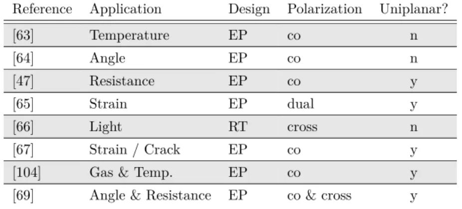
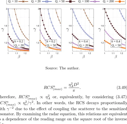
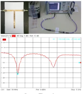
PVA based capacitive chipless sensors: (a) resonant frequency and (b) normalized resonant frequency as a function of the relative humidity of the environment. Simulated versus measured results of the normalized magnitude of the reflection coefficient to compare the resonant frequency.
MOTIVATION
Since this technology can participate in most applications, even the price of the tag's chip can be an obstacle to the demand for ultra-low-cost solutions. Driven by the promise of achieving low-cost wireless miniaturized sensors through chipless sensing, this technology was chosen to be the main driver of the current research.
RESEARCH SCOPE
In both architectures, the carrier frequency of the signal is swept and the backscattered wave from the tag is measured at each frequency step. In addition to the architecture of the reader, the antennas also play an important role in the reading strategy of the entire system.
RELATED STATE-OF-THE-ART STUDIES
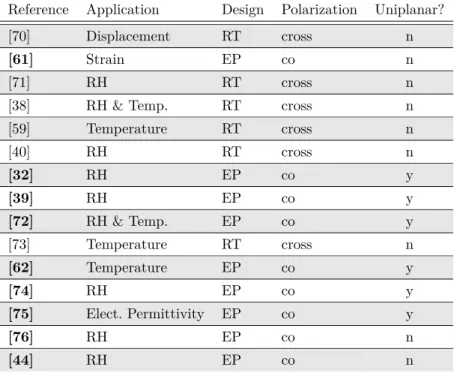
In addition, it is also observed that most of the sensors operate on the 2 to 6 GHz band, while higher frequencies have been investigated in a few cases. All the sensors carried his information about the shift of frequency where RCS peak occurred, except for the work in [62], which is based on slot resonators, and the work in [44], based on grounded loop resonators.
THESIS OBJECTIVES
DOCUMENT ORGANIZATION
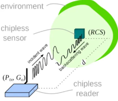
Analysis and experimental results of the effect of self-interference in low-profile chipless readers are left to Chapter 6. An important measure of the chipless system is the maximum read distance at which the backscattered EM waves reach the chipless reader with sufficient power to be correctly interpreted.
READING RANGE
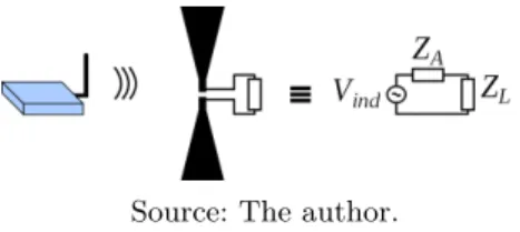
RADAR CROSS SECTION OF AN ANTENNA
Furthermore, it is important to emphasize that the structural mode is independent of the antenna loading. Finally, as mentioned above, the antenna mode term RCS depends on the radiation characteristics of the antenna.
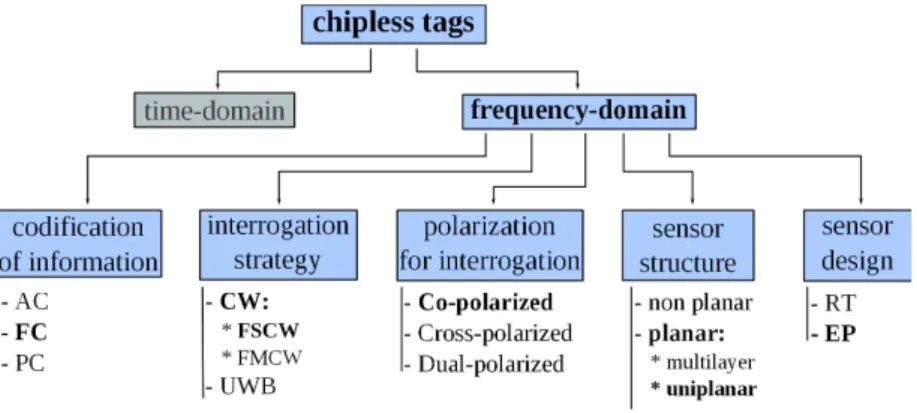
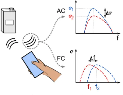
FIGURES OF MERIT OF CHIPLESS SENSORS
2.2, the transducer can be modeled either as part of the antenna or as the antenna load. As a result, the quality factor of the antenna can be related to the 3 dB bandwidth of the RCS frequency response.
RADIATION EFFICIENCY IN MINIATURIZED DIPOLE-BASED ANTENNAS
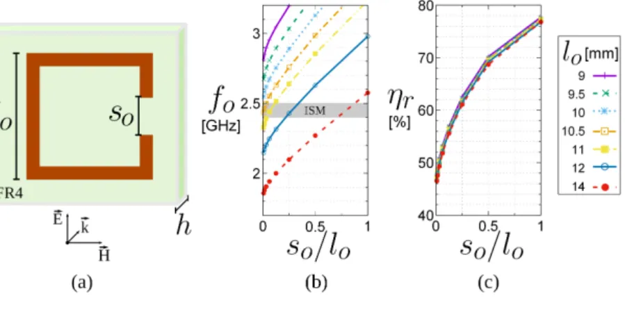
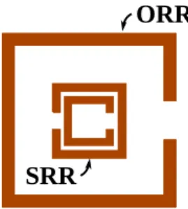
It can therefore be noted that, at resonance, the radiation resistance of the circular ORR depends exclusively on the slit angle. In this structure, the gap length of the ring (so) can be used to adjust the resonance frequency (fo) for a given lateral length (lo).
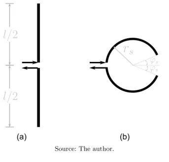
SPLIT-RING RESONATOR
Excitation of the SRR fundamental resonance can be achieved either by a time-varying perpendicular magnetic field or by an electric field parallel to the slits [92]. All the above features of the SRR can also be investigated in the integration of single-plane miniaturized backscattering-based sensors in which high sensitivity is required and where specific radiation properties must be well understood.
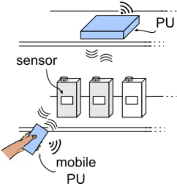
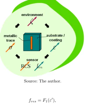
SENSOR CONCEPT
Therefore, this will lead to a new shifted resonance frequency (of the whole structure) higher than that of the scatterer. The new resonance frequency value would be such that the total inductance was equal to the self-capacitance of the scatterer.
EQUIVALENT ELECTRICAL MODEL
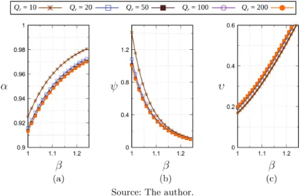
Making this substitution leads to the expressions where β is the normalized resonance frequency of the sensitized resonator (β=ωr/ωs=fr/fs). In addition, the distributor quality factor (Qs) can be used to quantify these losses.

SENSITIVITY ANALYSIS
Therefore, it can be stated that to estimate the total variation of the resonance frequency of the sensor, β|ε. From the plot on the left, it can be better observed that as the quality factor of the resonator decreases, the sensitivity decreases.
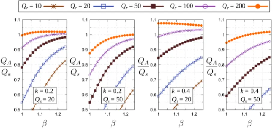
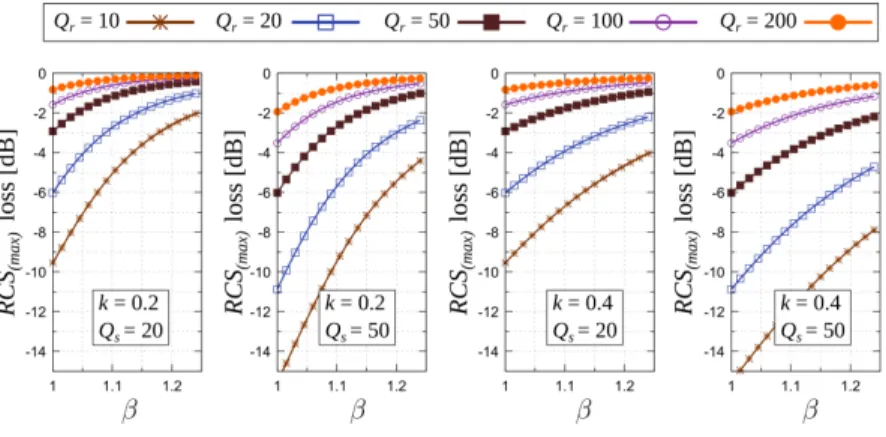
RADIATION EFFICIENCY ANALYSIS .1 Radiation efficiency calculation
Indeed, due to the increase of the real equivalent part of the diffuser, as observed from the results in the results of the graphs and the expression in (3.46), it should be expected that the radiation efficiency decreases. Finally, when the quality factor of the resonator exceeds that of the diffuser (Qr >> Qs), then γ≈1 and the radiation efficiency remains almost the same as that of the diffuser.
CHAPTER CONCLUSIONS
The sensor will benefit more from the sensitivity of the resonator since both resonances, of the scatterer and the resonator, are closer. Moreover, it is also positive from the point of view of the quality factor of the sensor as a whole.
STRUCTURE LAYOUT AND SIMULATION .1 Layout
In another way, in the above resonance subplots they start(end) at the ORR, but end(start) at the inner ring of the SRR. The first lines in the table correspond to the case of ORR (no transducer).
IMPLEMENTATION
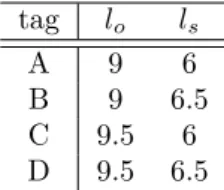
Therefore, a minimal gap of the ORR was considered. Based on the chosen set of dimensions and also in anticipation of possible inaccuracies during the manufacturing process of the structures, the final dimensions were chosen (shown in table 4.2). The SRR was sensitive to the humidity of the environment; in other words, the sensor was configured as an RH sensor.
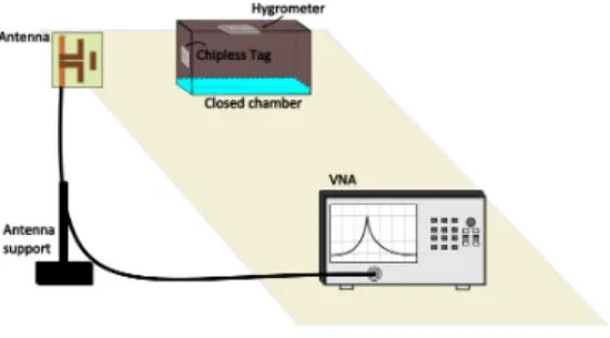
EXPERIMENTAL RESULTS .1 Measurement setup
The RCS of the sensor and its corresponding ORR (without coupled SRR) were measured before the PVA coating was applied. It was observed that the overall frequency shift (relative to its initial value) of the sensor is higher than in the ORR case.
CHAPTER CONCLUSIONS
In this scenario, a good sensitivity is still important, so that the sensor guarantees that the peak is out of band when needed. Finally, based on the results, some improvements in the design of the sensor are suggested and some experimental results are presented.
READING RANGE CONSIDERATIONS FOR THE DESIGN The design of a FD-FC low-cost chipless sensors should start with
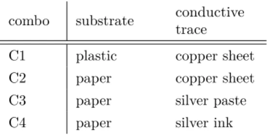
The results of the prototypes implemented with paper substrate are compared with other chipless sensors presented in literature fabricated with flexible substrate. However, this may not be the case if conductive materials with lower conductivity are to be used for the metal traces.
MATERIALS CHARACTERIZATION AND SIMULATIONS Flexible substrates are usually low-cost, conformable, and, in some
The main characteristics of the flexible substrates are summarized in Table 5.2, where FR-4 is included for comparison purposes. It is observed that the relative permittivity value of the plastic (PET) and the paper is very close.
IMPLEMENTATION AND EXPERIMENTAL RESULTS .1 Implementation
Another effect of this ratio is also appreciated in the lower quality factor of the sensors implemented in paper. The results were also consistent with the theoretical analysis of the sensor based on its electrical model.
CHAPTER CONCLUSIONS
Nevertheless, single-antenna setups are more prone to the self-interference effect1 due to the presence of an interference signal at the receiver chain caused by the leakage of the high-power output signal from the transmitter. However, in monostatic architectures the sensitivity term in the radar equation now becomes a function of the transmitted power.
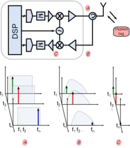
INTERFERENCE SOURCES IN CHIPLESS READERS In a typical reader with FSCW radar architecture as the one
Therefore, new theoretical expressions are needed for the maximum read range as a function of the SIC circuit performance when the reader is limited either by its noise floor, specifically the transmitter leakage noise, or by the dynamic range due to the transmitter leakage signal. Therefore, the main challenge for the reader is to distinguish the tag from these two interfering ones.
READING RANGE CONSIDERING THE TRANSMITTER LEAK- AGE AND A SIC TECHNIQUE
In addition to the impact of the transmitter leakage noise, the high power leakage signal must also be analyzed. For example, it is necessary that the down-converted signal is digitized with sufficient accuracy at the input of the digital processing unit.
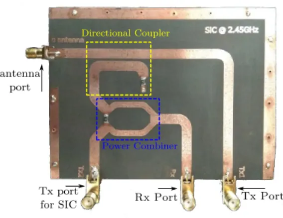
CASE STUDY
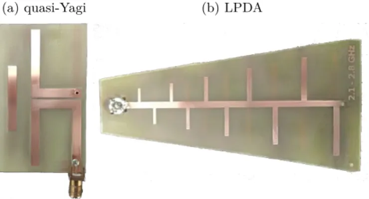
Measurements were taken at a distance of 20 cm from the tag in the center of the LPDA antenna. 6.9(a)), it can be seen that the curve corresponding to the first gain setting (D1) clearly showed the tag resonance valley.
CHAPTER CONCLUSIONS
CONCLUSIONS AND MAIN CONTRIBUTIONS
It was concluded that if the reader is looking to be low-cost and low-profile, requiring a monostatic single-antenna configuration, its read range will most likely be limited by the self-interference of its transmitter. First, when the reader is limited by the high power leakage signal from the transmitter.
FUTURE WORK
In this way, a theoretical analysis was carried out to determine the limits of the reading area, taking into account this question. Furthermore, further analysis of the antenna effect on the quality factor results is needed.
LIST OF PUBLICATIONS
Abstract: This paper presents the main results presented in Chapter 4, i.e. the full-wave simulation results and sensitivity measurements of the proposed sensor. Abstract: In this work, a study of the effect of self-interference cancellation in single-antenna monostatic chipless RFID readers on their read range was presented.
Appendices
RADIATION RESISTANCE OF AN ORR
Therefore, one can find the total radiation resistance by substituting the total electric dipole moment of the ORR into (A.10) from the result obtained in (A.9), and then dividing this expression by the current amplitude squared. In other words, it is demonstrated that, independent of the resonance frequency value, the radiation resistance is only dependent on the slit opening.
PARAMETER EXTRACTION FOR THE CIRCUIT MODEL For the estimation of the shifted frequency caused by the coupling
GENERAL CONSIDERATIONS
READER ANTENNA AND REFLECTOR SIZE
B.4, the theoretical RCS of the metal plates was used as reference (RCSplate= 4πA2/λ2, where A is the plate area). As a conclusion, it can be stated that for small reading distances, large metal plates can lead to erroneous RCS estimation of the tag.
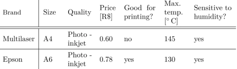
CONDUCTIVE INKS FOR INKJET PRINTED CIRCUITS Inkjet printers allow to use different solution-based materials,
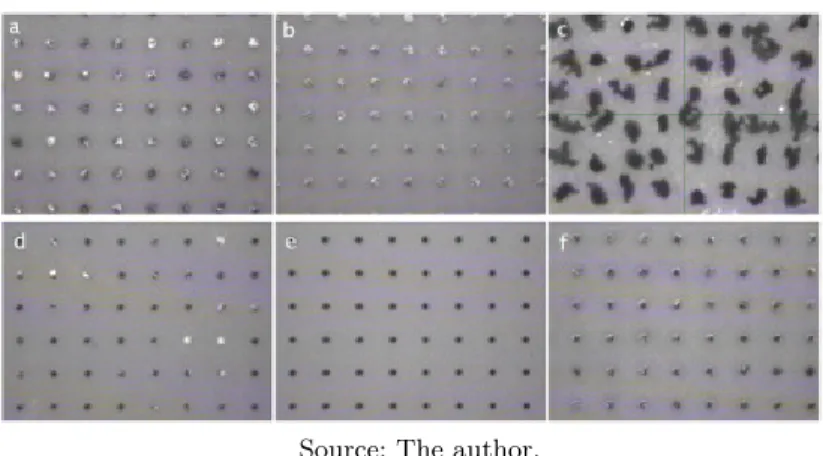
Photographs of pre-sintered and sintered squares taken with a fiducial camera are shown in Fig. Further analysis of the printed squares was done by measuring their thickness (and roughness) on a Detak profilometer.
DIELECTRIC PROPERTIES CHARACTERIZATION
Plots of the processed measurements are also shown, obtained from calculations in ADS software from Keysight. Simulated vs measured results of the normalized magnitude of the reflection coefficient to compare the resonance frequency.
FINAL DISCUSSION AND CONCLUSIONS
With regard to dielectric measurements, it can be deduced that it is very important that each type of paper is correctly characterized as they have different dielectric properties which directly affect the chipless tag design. It can also be used as a substrate for chipless tags or passive electronics in which the conductive traces are not printed, but a different type of material such as copper tape is used instead [149].