The State Space Average Model of
Buck-Boost Switching Regulator Including all of
The System Uncertainties
Mohammad Reza Modabbernia
Electrical Engineering Group, Technical and Vocational University, Rasht Branch Rasht, Iran
Fatemeh Kohani Khoshkbijari Sama Technical and Vocational Training College, Islamic Azad University, Rasht
Branch, Rasht, Iran [email protected]
Reza Fouladi Device and Process Modeling
and Simulation Lab Islamic Azad University,
Tehran South Branch Tehran, Iran [email protected]
Seyedeh Shiva Nejati Electrical Engineering Group
Sardar Jangal Higher Education Institute
Rasht, Iran [email protected]
Abstract—In this paper a complete state-space average model for the buck-boost switching regulators is presented. The presented model includes the most of the regulator’s parameters and uncertainties. In modeling, the load current is assumed to be unknown, and it is assumed that the inductor, capacitor, diode and regulator active switch are non ideal and they have a resistance in conduction condition. Some other non ideal effects look like voltage drop of conduction mode of the diode and active switch are also considered. This model can be used to design a precise and robust controller that can satisfy stability and performance conditions of the buck-boost regulator. Also the effects of the boost parameters on the performance of the regulator can be shown easily with this model. After presenting the complete model, the buck-boost converter Benchmark circuit is simulated in PSpice and its results are compared with our model simulation results in MATLAB. The results show the merit of our model.
Keywords-Buck-boost regulator; average model; SMPS; MATLAB; PSpice
I. INTRODUCTION
DC-DC Power converters are one of the standard components of switch mode power supplies (SMPS). They are used in personal computers, laptops, PDAs, office appliances, aircrafts, satellite communication equipment and DC motor starting circuits. The input of these converters is an unregulated DC voltage and its output is a regulated voltage [1].
In these converters, the switching capabilities of power devices are utilized to achieve the high efficiency. The non ideal nature of switches and their conduction mode resistance, and because the voltage and current can not suddenly become zero in switching times, there is some power loss on them. Due to these effects, the typical efficiency of such converters are actually about 70% to 95% [2].
Among the varieties of DC-DC converters, the Buck-boost regulator is used in applications where the output voltage should be higher than the input. In comparison with the other converters such as Buck or Buck-Boost, designing a controller for it is more difficult since this converter is a non minimum phase system and has a zero in the right half plan. In other words, since the control input of this converter (duty cycle of triggering pulse) is presented in both voltage and current equations, the state equations solution and controlling this regulator are more difficult [3].
The topology of DC-DC converters consists of two linear (resistor, inductor and capacitor) and nonlinear (diode and active switch) parts. Because of the switching properties of the power elements, the operation of these converters varies by time. Since these converters are nonlinear and time variant, to design a linear controller, we need to find a small signal model basis of linearization of the state space average model about an appropriate operating point of it. The small signal analysis and controller design in frequency domain for DC-DC converters are carried out by references [4-6].
work on buck-boost state space average model began in the 1970 decade by Cuke and Middlebrook [7], a model that consists of the aforementioned parameters was not presented.
Basso, Tomescue and Towati considered the boost regulator with inductance resistance, capacitance resistance and output current [8-10]. Benyakov only considers the capacitance resistance and output current regarding the said model and designs a robust controller. He mentioned the complexity of complete model and avoids presenting it in parametric form [11]. A linear model for Pulse Width Modulator(PWM) switch with an ideal diode and switch in both continuous and discontinuous current mode is presented in [12] and the effect of turn on resistance of diode and switch is considered in [13] for this model. An averaged model of boost regulator with consideration of capacitance and inductance resistances is demonstrated in [14]. Also, an average model to the PWM switch is presented by considering the diode and switch resistance and their voltage drop in discontinuous current mode without presenting the state space averaged model of regulator [15]. Finally, the state space average model of the boost regulator in the presence of all of the system uncertainties are presented in [16] and its P-Δ-K represented are introduced in [17].
In this paper, on the basis of state space average method, we first obtain the state space equations of a Buck-boost regulator in turn on and turn off modes by considering all the system parameters such as an inductor with resistance, a capacitor with resistance, a diode and switch on mode resistance and voltage drop, a load resistance and unidentified load current. Then the state equations are linearized around circuit operation point (input DC voltage and current versus output DC voltage). The coefficients of state space equations will therefore be dependent on the DC operating point in addition to the circuit parameters. At the end the duty cycle parameter “d” (control input) is extracted from the coefficients and introduced as an input.
Finally the buck-boost converter Benchmark circuit is simulated in PSpice and its results are compared with our complete model simulation results in MATLAB. The simulations were done in three scenarios. The results are very closed to each other.
II. BUCK-BOOST REGULATOR STATE EQUATUONS FOR ON-OFF TME SWITCHING
In modeling of the state space, the state variable which principally are the elements that store the energy of circuit or system (capacitance voltage and inductor current) have significant importance. In an electronic circuit, the first step in modeling is converting the complicated circuit, into basic circuit in which the circuit lows can be established. In switching regulators, there are two regions; the on region and off region. The on time denoted by d T, and the off time is denoted by d' T= (1-d) T, in which T is the period of steady state output voltage. “Fig.1” shows a buck-boost switching regulator. The switch is turned on (off ) by a pulse with a period of T and its duty cycle is d. Therefore we can represent the equivalent circuit of the system in two on and off modes with d T and d' T seconds respectively, by “Fig.2” and “Fig.3”.
Consideration iL and vC as our state variables (x = [iL vC]' ) and of writing the KVL for the loops of “Fig.2” we
will have:
Figure 1. Buck-boost regulator circuit
Figure 3. Equal circuit of Buck-boost regulator in off times
1 1
1 1
x A x B u
y C x D u
= + = + (1) G O L O out M c L D v v i i
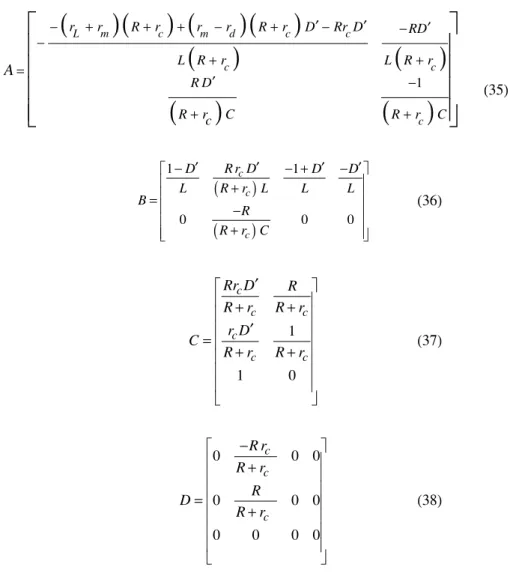
x u y i
v v i v = = = (2)
(
)
(
)
1 0 1 0 L m c r r L AR r C
− + = − + (3)
(
)
1 1 1 0 00 0 0
c
L L
B
R
R r C
− = − + (4) 1 0 1 0 1 0 c c R R r C R r + = + (5) 1
0 0 0
0 0 0
0 0 0 0
c c c R r R r R D R r − + = + (6)
2 2
2 2
x A x B u
y C x D u
= + = + (7) G O L O out M c L D v v i i
x u y i
v v i v = = = (8)
(
)
(
)
(
)
(
)
2 1c L L c d d c
c c
c c
Rr Rr r r Rr r r R
L R r L R r
A
R
R r C R r C
+ + + + − − + + = − + + (9)
(
)
(
)
2 1 0 00 0 0
c c c
R r
R r L L
B
R
R r C
− + = − + (10) 2 1 1 0 c c c c c c Rr R
R r R r r
C
R r R r
+ + = + + (11) 2
0 0 0
0 0 0
0 0 0 0 c c c R r R r R D R r − + = + (12)
The set of state equations “(1)” to “(12)” shows the state of buck-boost regulator in the on and off time of switch. We can combine these two set of equations as following [8,9]:
(
)
(
)
(
)
(
)
1 2 1 2 1 2 1 2 1 1 1 1 P p P PP P p
p
A A d A d
B B d B d
x A x B u
y C x D u C C d C d
D D d D d
= + − = + − = + = + = + − = + − (13)
(
)(
) (
)(
)
(
)
(
)
(
)
(
)
1
L m c m d c c
c c
P
c
r r R r r r R r d Rr d Rd
L R r L R r
R d
R rc C R r C
A ′ ′ − + + + − + − − ′ − + + = ′ − + +
(14)(
)
(
)
1 10 0 0
c c P
c R r d
d d d
L R r L L L
B
R
R r C
′ ′ ′ ′ − − + − + = − + (15) 1 1 0 c c c c P c c
Rr d R R r R r
r d C
R r R r
′ + + ′ = + + (16)
0 0 0
0 0 0
0 0 0 0 c c P c R r R r R D R r − + = + (17)
III. LINEARIZATION OF STATE EQUATIONS AROUND OPERATING POINT
The results presented in section2 are acceptable when the circuit time constant is much larger than the period of switching. . If the duty cycle be a constant value (d = D), the state equations in “(13)” will become linear. For regulating the voltage on a desired value, we have to change the value of D by a controller. In general, the state equations of “(13)” are nonlinear and we have to linear them around an operating point (D). When the system is in equilibrium and the duty cycle is on its nominal value (D), then we can obtain the system state values in equilibrium points (x = [IL VC]' ) and the DC output values .
1
0
G L O
P p P p
M C
D
V I I
x A x B u X A B
V V V − = + = = − =
(18)
(
)(
)
(
)
(
)(
)
(
)
(
) (
)
2 2(
)
(
) (
)
(
)
21 1
1 1
c c c c
G O M D
c c c c
G O M D
R r D R R r D R r D R r D
V I V V
X
R R r D D R D R r R R R r D D R R r D
V I V V
′ ′ ′ ′
+ − + + − +
+ −
Δ Δ Δ Δ
=
′ ′ ′ ′ ′ ′
+ − + − Δ + − +
+ −
Δ Δ Δ Δ
(
)(
) (
)
2 2L m c c d c d m m c
r r R r R r R r r r R r r r D′ R D′
Δ = + + + + + − − + (20)
And , O out p p L V I
Y C X D U Y
I = + = (21) Where
(
) (
)
2(
)
2(
) (
)
(
)
21 1
c c c c
O G O M D
R R r D D R R r D R R R r D D R R r D
V = + ′ − ′ V + + ′ − ΔI − + ′ − ′ V − + ′ V
Δ Δ Δ Δ (22)
(
) (
1)
(
)
2(
) (
1)
(
)
2c c c c
out G O M D
R r D D R R r D R r D D R r D
I = + ′ − ′ V + + ′ I − + ′ − ′ V − + ′ V
Δ Δ Δ Δ (23)
And
(
c)(
1)
(
c)
(
c)(
1)
(
c)
L G O M D
R r D R R r D R r D R r D
I = + − ′ V + + ′I − + − ′ V − + ′V
Δ Δ Δ Δ (24)
Finally for linearization of the system, on basis of classic method, we divided our variables into two parts. The first part is static part (a fixed DC level), and the second part is a small amplitude that modulates the DC level. On this basis, the variables in the state equations can be defined as follows:
ˆ ( ) ˆ ( ) ˆ ( ) ˆ ( )
o O o
x t X x
d t D d
u t U u
v t V v
= + = + = + = + (25)
In which VO, x = [iL vC]' and U = [VG IG VM VD]' are the nominal values of the DC output voltage, state
variables and no controllable inputs respectively. Each of them has small variations (denoted with ^ ) around nominal values. By substituting equations “(25)” in “(13)” and assumed that the duty cycle d has also variation dˆ
(d= D +dˆ), we will have
(
)
(
)
(
)
(
)
1 2 1 2
1 2 1 2
0
ˆ
ˆ ˆ ˆ
ˆ
ˆ ˆ ˆ
P P
O o P P O
X x A x B u A A X B B U d X
V v C x D u C C X D D U d V
+ = + + − + − + + = + + − + − + (26) Or
(
)
(
)
(
)
1 2 1 2
1 2
ˆ ˆ ˆ ˆ
, ˆ ˆ ˆ ˆ
P P
o P P
E A A X B B U
x A x B u E d
F C C X
v C x D u F d
= + + = − + − = − = + +
(27)
( ) ( ) ( ) ( )
(
)
(
)
( ) ( )
2 2 2
2 3 2 1
1 1 1
2
1 1
D K R D KD R D
K D R D D KR D R D R
V I V V
G O M D
L L L L
R D R D R D RD
V I V V
G O M D
C C C C
E
′ ′ ′ ′
− + + Δ + Δ
′ ′ ′ ′ ′
− + − + Δ − Δ
+ −
Δ Δ Δ Δ
=
′ ′ ′ ′
− − − −
+ + +
Δ Δ Δ Δ
− + − − (28) And
(
)
(
)
(
)
(
)
(
)
2 1 2 1 1 1 1c c c c
G O M D
c c c c
G O M D
R r D R r D R r D R r D
V I V V
F C C X
r D Rr D r D r D
V I V V
− − ′ − ′ − ′ ′
+ + +
Δ Δ Δ Δ
= − = − − ′ − ′ − ′ ′ + + +
Δ Δ Δ Δ
(29)
With
c d d c c m m
K=Rr +Rr +r r −r r −Rr (30)
And Δ is defined by “(20)”.
IV. STATE SPACE AVERAGE MODEL
An important point in the set equations in that APand CP are related to d'=1-d. Since d = D +dˆthen AP and
CP are related todˆ. It can be shown that with good approximation this dependence is negligible. By sub situation
AP, BP, CP and DP by their equivalents in term of d, A1, B1, C1 and D1 we will obtain:
(
)
[
]
[
(
)
]
(
)
[
]
[
(
)
]
1 2 1 2
1 2 1 2
ˆ
ˆ 1 ˆ 1 ˆ
ˆ
ˆ 1 ˆ 1 ˆ
x A d A d x B d B d u E d
y C d C d x D d D d u F d
= + − + + − + = + − + + − + (31)
d = D +dˆ therefore, we have for the first above equation.
(
)
(
)
(
)
(
)
1 2 1 2 ˆ 1 2 ˆ 1 2 ˆ
ˆ 1 ˆ 1 ˆ ˆ ˆ
x=A D+A −D x+B D+B −D u+E d+ A −A d x+ B −B d u (32)
Since dˆ, uˆand xˆdenotes small variation of the duty cycle, input and state of system respectively, their product is very small and we can neglect terms such asd xˆ ˆandd uˆ ˆ.
ˆ ˆ ˆ ˆ
x=A x+B u+E d (33)
In the same manner, the effect of d xˆ ˆ and d uˆ ˆ in second equation of “(32)” is negligible. Therefore we can represent the buck-boost regulator state equations like this:
ˆ
ˆ ˆ ˆ
ˆ
ˆ ˆ ˆ
ˆ L ˆ ˆ
C G O O out M L D i
x A x B u E d
v
y C x D u F d
v
v i
i
x u y
v i v = + + = = = + + =
(
)(
) (
)(
)
(
)
(
)
(
)
(
)
1
L m c m d c c
c c
c
r r R r r r R r D Rr D RD
L R r L R r
R D
R rc C R r C
A
′ ′
− + + + − + − − ′
−
+ +
=
′ −
+ +
(35)
(
)
(
)
1 1
0 0 0
c c
c R r D
D D D
L R r L L L
B
R
R r C
′
′ ′ ′
− − + −
+
=
−
+
(36)
1
1 0
c
c c
c
c c
Rr D R
R r R r
r D C
R r R r
′
+ +
′
= + +
(37)
0 0 0
0 0 0
0 0 0 0
c c
c R r R r R D
R r
−
+
=
+
(38)
Eand F are represented with equations “(28)” , “(29)” respectively.
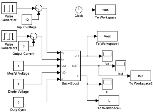
V. SIMULATION WITH PSPISE AND MATLAB
To show the accuracy of our complete model, we simulate the buck-boost benchmark circuit with PSpice and then compare its consequences with the simulation results of presented model in MATLAB. “Fig. 4”, “Fig. 5” and “Fig. 6” show the buck-boost benchmark circuit in PSpice and its equivalent model in SIMULINK respectively. The simulations were performed under the following conditions: L = 200 μH, C = 220 μF, R = 44 Ω, rm=rd=rC = 0.1Ω, rL = 0.2 Ω and VG = 12 V. The switching frequency is 240 kHz and various cases of simulation
have been considered. In the first case, the forward voltage drop of the active switch accompanied by the load current and the diode voltage drop have been reckoned zero and 0.1 V respectively. In the second case, the voltage drop of the diode and active switch, and also load current are 0.1 V, 0 V and 1 A respectively. Finally, with the consideration of forward voltage drop equal to 1 V for the diode and active switch, a sudden change of 5V in the input voltage and 3 A in the output current have been taken into account for the converter.
Figure 5. The buck-boost benchmark circuit in SIMULINK
Figure 6. Equivalent model of Buck-boost regulator in SIMULINK
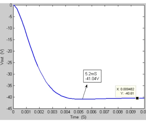
A. Switches with no forward voltage drop and I0 = 0 A
Figure 7. Output voltage with IO = 0 A, VD= 0.1 V and VM= 0 V in PSpice
Figure 8. Output voltage with IO = 0 A, VD= 0.1 V and VM= 0 V in MATLAB
TABLE I. COMPARING THE RESULTS WITH IO=0A,VD=0.1VAND VM=0V
Output Voltage Overshoot
PSpice Between -40.451
and -40.994 -41.387V
MATLAB -40.61 -41.04V
B. Active switch with VM= 5.7 V and IO= 1 A
The results of simulation with IO = 1 A, VD =0.1 V and VM =5.7 V are shown in “Fig. 9” and “Fig. 10”.
VM=5.7 V is the drain source voltage drop of IRF540 MOSFET in PSpice. The table II shows these simulation
Figure 9. Output voltage with IO = 1 A, VD= 0.1 V and VM= 5.7 V in PSpice
Figure 10. Output voltage with IO = 1 A, VD= 0.1 V and VM= 5.7 V in MATLAB
TABLE II. COMPARING THE RESULTS WITH IO=1A,VD=0.1VAND VM=5.7V
Output Voltage Overshoot
PSpice Between -21.211
and -21.487 -21.702V
MATLAB -21.28 -21.5V
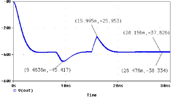
C. 5V and 1A disturbances in the input voltage and load current
If we consider a BJT transistor like 2N6546 instead of IRF540 MOSFET, we will have a 1 V voltage drop on the collector-emitter of transistor. The results of simulation with IO= 0 A and VD=VM=1 V are shown in “Fig.11”
Figure 11. Output voltage with VD= VM= 1 V in PSpice. There are a 5V and 1A disturbances in input voltage and load current respectively
Figure 12. Output voltage with VD= VM= 1 V in MATLAB. There are a 5V and 1A disturbances in input voltage and load current
respectively
TABLE III. COMPARING THE RESULTS WITH VD=VM=1V .THERE ARE A 5VAND 1ADISTERBANCES IN INPUT VOLATGE AND
LOAD CURRENT RESPECTIVILY
Output Voltage Input Voltage Overshoot
Load Current Overshoot
PSpice Between -37.826
and -38.334 -45.417V -25.9537V
MATLAB -36.46 -43.45V -24.97V
VI. CONCLUSION
an average model is presented for buck-boost regulator with all of the above uncertainties. By neglecting some of them, we can easily convert this complete model to any other simple model. Also by converting it to the P-Δ-K configuration, we can analyze any linear controller by μ-synthesis theorem. Finally, the buck-boost converter Benchmark circuit is simulated in PSpice and its results are compared with our model simulation results in MATLAB. The results are so closed to each other.
REFERENCES
[1] N.Mohan, T. M. Undeland, and W. P. Robbins, “Power Electronics, Converters, Applications, and Design,” John Wiley & Sons, 2003. [2] R. Erickson, “DC-DC Converter,”Article in Wiley Encyclopedia of Electrical and Electronics Engineering.
[3] V. I. Utkin, “Sliding Mode Control Design Principles and Applications to Electric Drives,” IEEE Trans. On Industrial Applications, Vol. 40, pp. 23-36.
[4] J.H. Su, J.J. Chen, and D. S. Wu, “Learning Feedback Controller Design of Switching Converters via MATLAB/SIMULINK,” IEEE Trans. On Education, Vol.45, pp. 307-315, 2002.
[5] J R. B. Ridley, “A New Continuous-Time Model for Current –Mode Control,” IEEE Trans. On Power Electronics, Vol. 6, No. 2, PP. 271-280, 1991.
[6] P. Li, and B. Lehman,“A Design Method for Paralleling Current Mode Controlled DC-DC Converters,” IEEE Trans. On Power Electronics, Vol. 19, PP. 748-756, May 2004.
[7] R.D. Middlebrook, and R S.cuk., “A General unified Approach to Modeling switching converter power stages," IEEE PESC, Record, PP 18-34, 1976.
[8] F. Alonge, F. D’Ippolito, and T. Gangemi, “Identification and Robust Control of DC/DC Convertor Hammerstein Model”, IEEE Transaction on Power Electronics, Vol. 23(Issue6), November 2008.
[9] B. Tamescu, “On the Use of Fuzzy Logic to control Paralleled DC-DC Converters,” PHD Thesis, Blackbury, Virginia Polytechnic Institute and State University, October 2001.
[10] A.Towati, “Dynamic Control Design of Switched Mode Power Converters,”Doctoral Thesis, Helsinki Jniversity of Technology, 2008. [11] R. Naim, G. Weiss, and S. Ben-Yaakov, “H∞ Control Applied to boost Power Converters,” IEEE Trans. On Power Electronics, vol.
12, no. 4, pp. 677-683, July 1997.
[12] V. Vorperian, “Simplified Analysis of PWM Converters Using the Model of the PWM Switch,Parts I (CCM) and II (DCM),” Trans. On Aerospace and Electronics systems, vol. 26, no. 3 May 1990.
[13] V. Vorperian, “Fast analytical techniques for Electrical and Electronics Circuits,” Cambridge University Press, 2004, ISBN 0-521-62442-8.
[14] A. Romero, “Circuito Integrade de Control Deslizante Para Convertidores Conmutados Continua”, Thesis Doctoral (en Realizacion). Department d’Enginyeria Electeronica Universital Polictecnica de Catalunya.
[15] C. M. Ivan, D. Lascu, and V. Popescu, “A New Averaged Switch Model Including Conduction Losses PWM Converters Operating in Discontinuous Inductor Current Mode,” SER. ElEC ENERG. Vol. 19, No. 2 , PP 219-230, August 2006.
[16] M. R. Modabbernia, A. R. Sahab, M. T. Mirzaee, and K. Ghorbani, “The State Space Average Model of Boost Switching Regulator Including All of the System Uncertainties,” Advanced Materials Research, Vol.4-3-408, pp 3476-3483, 2012.
[17] M. R. Modabbernia, A. R. Sahab, and Y. Nazarpour, “P-Δ-K Model of Boost Switching Regulator with All of The system Uncertainties Based On Genetic Algorithm,” International Review of Automatic Control, Vol. 4, No. 6, November 2011.
AUTHORS PROFILE
Mohammad Reza Modabbernia was born in Rasht, IRAN, in 1972. He received the B.S. degree in Electronics Engineering and M.S. degree in control engineering from KNT, the University of Technology, Tehran, IRAN in 1995 and 1998 respectively. He is the staff member of Electronic group of Technical and Vocational university, Rasht branch, Rasht, IRAN. His research interests include Robust Control, Nonlinear Control and Power Electronics.
Fatemeh Kohani Khoshkbijari was born in Rasht, Iran in 1982. She received her B.Sc. degree in electrical engineering from Islamic Azad University of Lahijan, Lahijan, Iran, in 2005 and the M.Sc. degree in Electrical Engineering from Islamic Azad University Tehran South Branch, Tehran, Iran, in 2008. As a novel research in nanotechnology, her M.Sc. thesis was awarded by Iranian Nanotechnology Initiative Council. She is a university lecturer at Sama Technical and Vocational Training College, Islamic Azad University, Rasht Branch since 2009. Her research interests include Low Power Design, Device Physics, Process/Device Design, CAD Development for Process and Device Design, Simulation, Modelling and Characterization of Nanoscale Semiconductor Devices.
Reza Fouladi was born in Rasht, Iran in 1978. He received the B.S. degree in Electrical Engineering in 2002 from Guilan University and M.Sc. degree in Electronics from Islamic Azad University Tehran South Branch in 2006. His research interests include simulation and Modelling of nanoscale devices and quantum transport in devices.