A Modified Hardware Efficient Watermarking Scheme
for Intellectual Property Protection in Sequential
Circuits
Jeebananda Panda, Siddhant Malik, Neeta Pandey, Asok Bhattacharyya
Abstract – This paper presents a modified scheme for intellectual property protection in sequential circuits by embedding watermark in state transition graph in order to prove ownership in case of intellectual property theft. The hardware requirement, in general, increases for designs which are watermarked. The proposed scheme is hardware efficient than the existing scheme. The proposed scheme is illustrated through an example of a six bit sequence detector. The workability of the scheme is demonstrated by simulating RTL using VHDL simulators. The performance comparison with the existing scheme indicates that the proposed scheme is hardware efficient than the existing one.
Keywords –FSM, Intellectual Property Protection, VLSI, Watermark, Signature.
I. I
NTRODUCTIONWith electronics industry witnessing stupendous growth in the last decade, cases where intellectual property theft has increased manifold. With the advancement in technology, design automation tools have become important and integral part of the electronics industry. It is imperative to test the design using simulation tools before actual fabrication. The simulation tools generate files which are transferred to the foundry for the next step i.e. fabrication. These files can be easily stolen if one has access to the workstation of the researcher. Such a theft can’t be prevented but it is possible to prove the ownership of the “stolen intellectual property” with the help of watermarking technique. There are significant research efforts towards addressing various issue in watermarking as is evident from the literature [1-10] and references cited therein.
In this paper the embedding of watermark in state transition graph of a sequence detector (taken as an example of sequential circuit) as a measure to prove the ownership of intellectual property has been discussed. Oliveira [5,6] proposed a methodology that can be efficiently used to prove ownership of the sequential circuits. The watermark is embedded by introducing duplicate states [5,6] in the State Transition Graph (STG) of the circuit whereas redundant state transitions are used for watermarking in [7]. The techniques proposed in [5,6,7] are robust and non-detectable. Any sort of tampering with the watermark would in turn cause the loss of functionality. Hence, making it tamper proof. The approach [8] focuses on modeling regular sequential functions as finite state machines and exploiting some unutilized input vectors. Modifications were introduced so as to trigger a specific response with known input excitations. It was shown how the odds of reproducing
identical behavior can be made arbitrarily small. It was also demonstrated how machines, which have been infringed upon, are effectively detected. E. Charbon [9] puts forward the concept of hierarchical watermarking for IC design. The techniques have been proposed for the synthesis and detection, and to quantify its resilience to engineering modifications. The paper proposes basic algorithms for generation of watermark at various abstraction levels in IC design. These algorithms are tested for robustness against forgery. The paper [10] addresses the issue of high security risks whenever Intellectual property (IP) blocks are reused for facilitating the design process of System-on-a-Chip. The current state-of-art schemes for this purpose are explained and compared. It also includes discussion on the major considerations such as embedding cost, probability of co-incidence etc.
This paper addresses the problem of implementing watermarking in sequential circuits and puts forward a modification to classical Oliveira approach. The proposed approach is more efficient than the existing approach in terms of hardware requirement. This paper is organized in five sections. Section II briefly reviews the classical Oliveira approach followed by the detailed description of the proposed approach. An example of 6-bit sequence detector is taken for demonstration. The implementation scheme is given in Section III. The functional verification of proposed scheme is carried out through VHDL simulation. An analysis and comparison of the results for both the watermarked and non-watermarked state machines is detailed in Section IV followed by conclusion in section V.
II. D
ESCRIPTION OFO
LIVIERAA
PPROACH AND THEM
ODIFIEDA
PPROACHCopyright © 2014 IJECCE, All right reserved related to the increase in hardware requirement which
translates to larger area on the chip therefore the designer has to look for opportunities for hardware optimization. Thus embedding of watermark should be both invisible and hardware efficient.
A six bit sequence detector to detect the sequence “100111” is taken as an example to demonstrate watermarking in sequential circuits. The sequence detector is designed as a Mealy machine and its STG is depicted in Fig.1 which has six states {a, b, c, d, e, f}. The detailed description for designing a sequential circuit as a Mealy machine is given in Appendix 1. These six states are referred to as “original states” for further discussion in this paper. The process of watermarking is explained with help of embedding a signature “110” in STG using both the Oliveira [5,6] and the proposed approach.
The technique proposed by Oliveira [5,6] embeds watermark in the STG by duplicating the original STG and adding watermark detection states. The reasons why these additional states are added are described
below:-(i) Duplication of original states:- For the sequential machines watermarked with the approach proposed by Oliveira it is essential to duplicate the original states when designing the STG of the watermarked machine. This is necessary because of the fact that the control from the watermark detection states never shifts back to the “original states”. That is why to meet the first and foremost requirement of watermarking that the watermarked machines and non-watermarked machines be similar functionally, the duplicate states are added to conserve the functionality of the non-watermarked machine.
(ii) Watermark Detection States:- These states are required because of the fact that whenever watermark sequence will be asserted at the input of the sequence detector, these states will be traversed and hence will be instrumental in proving the ownership of the machine under consideration. The step by step description of Oliveira’s approach for two different scenarios is as
follows:-(i) Watermark sequence not present at the input:-It is the case when the input to the sequence detector does not contain the watermark sequence. In this case the original states will be the only ones that will be traversed and control won’t move to the watermark detection states. The output in this case would solely depend upon traversal of original states.
(ii) Watermark Sequence Present at the input:-It is the case when the watermark sequence is present in the input to the sequence detector. In this case the control shifts from original states{a,b,c,d,e,f} to the watermark states{r,s,t}. It is important to note here that the control will be transferred from the watermark states to the duplicate states {g,h,i,j,k,l} and not to the original states in this case. In this case the output would solely depend upon traversal of duplicate states. Since, the duplicate states are essentially similar in design to the original states the behavior of the machine will be identical to the machine without watermark.
To illustrate the above two points with an example, let us consider an input sequence “1001111”. The sequence
detector of Fig.1 traverses through {a, b, c, d, e, f, b} upon assertion of “1001111” at its input. Since this sequence begins with a ‘1’ which is part of signature, the control in STG of Fig. 2 initially shifts to the watermark states and the detector routes through {a, r, i, j, k, l, r}. It confirms the above two points, that once the control is with watermark states it will shift to the duplicate states and not the original states [Fig. 2]. The output of ‘1’ is asserted on detection of the “100111” for sequence detectors of Figs. 1 and 2 but different set of states are traversed. Thus, the technique proposed by Oliveira fulfils the first requirement that watermarked machine and the machine which doesn’t have watermark are functionally similar. The watermark is completely hidden which is proven by the fact that both the watermarked and non-watermarked machines are identical in behavior to any input sequence. However, the technique proposed by Oliveira is hardware intensive i.e. requires a larger area on the chip which is discussed in section IV and consumes more power.
Fig.1. Original S.T.G for 6-bit sequence detector. The proposed method modifies the original STG by including only signature states. Fig.3 shows the machine designed with the proposed approach. The step by step procedure to design the watermarked sequential circuit using the proposed approach is as
under:-(i) The number of original states is determined from the number of bits in sequence to be detected i.e. for a six bit sequence detector there will be six original states in the sequence detector. The original states are labeled as {a,b,c,d,e,f}.
(ii) The number of states that detect the watermark sequence will depend on the number of bits in watermark. (iii)The STG is redesigned in such a way that whenever the input contains watermark sequence, the traversal is made through watermark states. The control shifts back to the original states on complete traversal of the watermark states.
Fig.2. Modified S.T.G. for 3-bit watermarked sequence detector according to the technique proposed by Oliveira
[5,6].
Keeping the procedure to design watermarked machine using the proposed scheme in mind, the original STG of Fig1 is modified and redesigned in Fig.2. To illustrate the functionality of the watermarked machine designed with the proposed approach with an example, we will consider an input sequence “1001111”. Since this sequence begins with a ‘1’ and not a ‘0’ the control initially shifts to the watermark states and the detector routes through {a, r, c, d, e, f, r}. The output of ‘1’ is asserted from the sequence detector on detecting the sequence “100111”. For the same input sequence “1001111”, the sequence detector of Fig.1 behaves in an identical manner externally that is the output of ‘1’ is asserted on detection of the “100111” but internally a different set of states are traversed. The sequence detector of Fig.1 traverses through {a, b, c, d, e, f, b} upon assertion of “1001111” at its input. Thus, the technique proposed in this paper fulfils the first requirement that watermarked machine and the machine which doesn’t have watermark arefunctionally similar. The watermark is completely hidden which is proven by the fact that both the watermarked and non-watermarked machines are identical in behavior to any input sequence. However, the technique proposed in this paper embeds the watermark in a more efficient manner when compared in terms of hardware requirement. A close observation of Fig.2 and Fig.3 reveals that the technique proposed in this paper uses only nine states against the fifteen states required by the technique proposed by Oliveira and therefore requires lesser hardware(refer to section IV) than
the existing technique. This translates into lesser on chip area and power consumption when compared with the existing technique.
Fig.3. Modified S.T.G. for 3-bit watermarked sequence detector using proposed technique
III. I
MPLEMENTATIOND
ETAILSThe STGs of Figs. 1-3 are implemented in order to show the usefulness of the proposed scheme. The RTL schematic shown in Fig.4 is used for illustration. The circuit is modeled using VHDL. The original states {a,b,c,d,e,f} are assigned numbers from 1-6; whereas the numbers 7-12 are given to duplicate states {g, h, i, j, k. l}i.e. state ‘l’ corresponds to number 12. Numbers are used for representing state transitions in order to have one more level of security because only the designer will be able to tell which state corresponds to which number. The signature states {r, s, t} are numbered as ‘13, 14, 15’ i.e. ‘r’=13; ‘s’= 14 and so on.
Fig.4. RTL schematic for 6-bit sequence detector {watermarked and non-watermarked}.
IV. S
IMULATIONR
ESULTSCopyright © 2014 IJECCE, All right reserved Report. In order to show similarity in the functionality, an
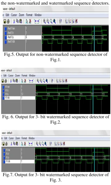
input sequence of “100111” is applied to the STGs of non -watermarked sequence detector; the sequence detector watermarked with 3-bit signature using the existing approach and proposed approach. The corresponding results are shown in Figs. 5 -7. It may be noted that the output is exactly the same for the same input sequence i.e. there is no difference in the outputs from watermarked and non-watermarked sequence detectors, hence no difference as far as functionalityis concerned, and thereby achieving our foremost goal that watermark is not detectable. However, there is a striking difference between the states which are being traveled for the same input sequence for the non-watermarked and watermarked sequence detectors.
Fig.5. Output for non-watermarked sequence detector of Fig.1.
Fig. 6. Output for 3- bit watermarked sequence detector of Fig.2.
Fig.7. Output for 3- bit watermarked sequence detector of Fig. 3.
In order to show the traversal of signature states for STG of Fig. 2 and 3, a sequence “1100111” (“110” is the signature) is inputted to the machines and the output is shown in Figs. 8 and 9 respectively. It may be observed that upon receiving the input of sequence“110” the states traversed are “13, 14, 15” which correspond to states {r, s, t} respectively for both cases. Thus, the claim of watermarking of machine is proved.
The hardware requirements of different machines are compared by synthesizing the VHDL code for the STGs of Figs. 1 – 3, the result is given in Table 1. Following observations are made from data provided in Table 1.
Fig. 8 Output for 3- bit watermarked sequence detector of Fig.2 for “1100111”
Fig.9. Output of proposed 3- bit watermarked sequence detector for “1100111”
1. Flip-Flops Requirement:-From the table1 given in the post synthesis report section the number of low density flip flops required for the non-watermarked sequence detector is the lowest i.e. 10 and it is highest for the 3-bit watermarked sequence detector for the existing technique i.e. 20. The proposed technique reduces the number of flip flops to 14 against 20 for the existing technique [5,6]. 2. Cell Usage: - The number of cells used for the non-watermarked sequence detector is the lowest i.e. 12. The 3-bit watermarked sequence detector designed with the existing technique [5,6] highest i.e. 30 whereas the one designed with proposed technique uses only 19 cells. 3. The number of IOs, IO buffers and the number of clock buffers are the same for all the three machines. Thus all the machines are identical as seen from outside i.e. even if they have different internal configuration they are all identical in appearance to the user.
Further, it may be noted that the number of output buffers may be reduced significantly (to two from five) by using a combinational detection circuit that detects the last signature state. To elaborate it further, let us consider that an input sequence “1101” is applied then watermark states would be traversed. Once the state‘t’ is reached, the detection circuit would indicate that watermark has been traversed.
Table 1: Hardware requirements
Component Details
Details of Type of Machine
Non-watermarke
d sequence detector
3-bit watermarked
sequence detector [5,6]
3-bit watermarked
sequence detector [proposed ]
FLIP-FLOPS 10 {LD} 20 {LD} 14 {LD}
IOs 7 7 7
CELL
USAGE 12 {BELS} 30 {BELS} 19 {BELS}
CLOCK Buffers
1
{BUFGP} 1 {BUFGP} 1 {BUFGP}
IO Buffers 1{IBUF} 5{OBUF}
1{IBUF} 5{OBUF}
The results of timing analysis are given in Table 2. The maximum operational frequency for the watermarked machines with the existing techniques is slightly less as compared to the sequential machine without watermark. But, with the technique proposed and implemented in this paper the maximum operational frequency is very close to the machine without watermark. This is the major accomplishment of our work.
Table 2: Timing details
Timing and Frequency Criteria
--Details of Type of Machine
Non-watermarked
sequence detector
3-bit watermarked
sequence detector
[5,6]
3-bit watermarked
sequence detector [proposed ] Minimum
input arrival time before clock
3.789ns 4.554ns 4.014ns
Maximum
Frequency 214.29MHz 178.52MHz 209.84MHz Maximum
output required time after clock
6.897ns 6.897ns 6.897ns
V. C
ONCLUSIONA modified scheme for embedding watermarks in state transition graph is presented in this paper. The proposed scheme reduces the hardware requirement in comparison to the existing technique. The workability of the proposed scheme is illustrated through six bit sequence detector. VHDL simulations using VHDL simulators are included to prove the claim of embedding the watermark in the STG with minimal hardware overhead and at the same time keeping the watermarked machine similar in behavior to the non-watermarked machine. Further, the maximum frequency of watermarked circuits with this proposed scheme found to be much higher than that of classical Oliveira [5,6] technique.
A
PPENDIXIn this paper all the state transition diagrams for sequence detectors are designed using mealy machines. Mealy machines are a set of finite state machines where the output ‘z’ from the machine is dependent on the current state ‘y’ and the present input ‘x’ to the machine. In this paper the current states ‘y’ are represented as:
-Original State Name Encoded State Number
a 1
b 2
c 3
d 4
e 5
f 6
g 7
h 8
i 9
j 10
k 11
l 12
r 13
s 14
t 15
In this paper the current input ’x’ is of one bit i.e. it can be either 0 or 1. Depending upon x and y the output z is asserted. In this paper the output z is of one bit i.e. 0 or 1. The figure below shows a basic mealy machine.
Here states ‘y’ are represented as S(i) and state transitions are represented by arrows connecting from one state to another. From the figure above it is clear that the state transition from one state to another is dependent on the present input (shown in red). The output ‘z’ is represented in blue on top of the arrow showing state transition. This is the standard representation while drawing state transition graph for a mealy machine. The same is followed in this paper.
Design of a Sequence Detector as a Mealy Machine
The procedure to design a sequence detector as a Mealy machine is discussed with an example of a five bit sequence detector. The steps for the design of a sequence detector are listed asunder:-1. Determine the Type of sequence detector:- It is also important to decide the type of sequence detector to be designed. There are two types of sequence detectors:-a. Overlapping Sequence Detectors:- In an sequence detector that allows overlap, the final bits of one sequence can be the start of another sequence. The output for an overlapping sequence detector that detects “11011” for an input of X=11011011011 is Z=00001001001.
b. Non-Overlapping Sequence Detectors:- In an sequence detector that does not allow overlap, the final bits of one sequence cannot be the start of another sequence. The output for a non-overlapping sequence detector that detects “11011” for an input of X=11011011011 is Z=00001000001.
For our explanation we will take the design of an overlapping sequence detector.
Copyright © 2014 IJECCE, All right reserved our example the sequence detector detects a six bit
sequence “11011”. Hence the total number of states would be five. We label these states A, B, C, D, and E. State A is the initial state.
3. Characterize Each State by What has been Input and What is Expected
:-State Has Awaiting
A -- 11011
B 1 1011
C 11 011
D 110 11
E 1101 1
4. Do the Transitions for the Expected Sequence. Shown here is a partial drawing of the state diagram. It has only the sequence expected. Note that the diagram returns to state C after a successful detection; the final 11’s are used again.
5. Insert the Inputs That Break the Sequence.
6. Hence, we have successfully shown the design of a five bit sequence detector.
R
EFERENCES[1] S. M. Mousavi, A.Naghsh, S. A. R. Abu-Bakar, “Watermarking Techniques used in Medical Images: a Survey,” Journal of Digital Imaging, DOI 10:1007/s10278-014-9700-5.
[2] M. Ghebleh, A. Kanso and H. S. Own,“A blind chaos-based watermarking technique Security and Communication Networks,7, pp. 800–811, 2014.
[3] P. Prathik, R. Krishna, R. A. Nafde, K. Shreedarshan, “An Adaptive blind video watermarking technique based on SD-BPSO and DWT-SVD,” 2013 International Conference on Computer Communication and Informatics (ICCCI), pp 1 -6. [4] W. Liang, X. Sun, Z. Ruan, J. Long, , C.Wu, “A Sequential
Circuit-Based IP Watermarking Algorithm for Multiple Scan Chains in Design-for-Test,” Radioengineering, 20, pp.533-539, 2011.
[5] A. L. Oliveira, "Techniques for the Creation of Digital Watermarks in Sequential Circuit Design,” IEEE Transactions on Computer-aided Design of Integrated Circuits and Systems, Vol. 20, no. 9, pp.1101-1117, 2001.
[6] A. L. Oliveira, “Robust Techniques for Watermarking Sequential Circuit Designs,” Proc. IEEE/ACM Design Automation Conf., pp.837–842, 1999.
[7] A. Cui, C. H. Chang, , S. Tahar, and A. T. Abdel-Hamid, “A Robust FSM Watermarking Scheme for IP Protection of Sequential Circuit Design,” IEEE Transactions on Computer-Aided Design of Integrated Circuits and Systems, 30, pp. 678– 690, 2011.
[8] J. Toruoglu, and E. Charbon, "Watermarking Based Copyright Protection of Sequential Functions,” IEEE journal of Solid State Circuits, Vol. 35, no. 3, pp. 434-440, 2000.
[9] E. Charbon, “Hierarchical Watermarking in IC Design,” Proc. IEEE Custom Integrated Circuit Conf., May 1998, pp. 295–298. [10] A. T. Abdel-Hamid, S. Tahar and E M. Aboulhamid, “IP
Watermarking Techniques- Survey and Comparison,” Proceedings of The 3rd IEEE International Workshop on System-on-Chip for Real-Time Applications, pp. 60-65, , 2003.
A
UTHOR’
SP
ROFILEJeebananda Panda
Born on 15 th Feb, 1968 in Odisha , India . He got graduated in Electrical engineering and subsequently in electronics and Communication engineering in 1988 and 1989 respectively. He got his M.E degree in Applied Electronics specialization from Bharathiyar University in 1992. Presently working as Associate Professor in the Department of Electronics and Communication Engineering, Delhi Technological University, Delhi, India. He is working for Ph.D in Dept. of Electronics in Engineering, Faculty of Technology, Delhi University. His field of research is Watermaking of Digital Data.
Siddhant Malik
Siddhant completed his B.E. in Electronics and Communication Engineering from Delhi College of Engineering,Delhi in June,2013. He has a keen interest in designing high end cameras for smartphones, processors and cache design for high performance CPU's. He is currently working as a Camera Hardware Design Engineer with Qualcomm, Bangalore.
Neeta Pandey
Completed M.E. in Microelectronics from Birla Institute of Technology and Sciences, Pilani and Ph.D. from Guru Gobind Singh Indraprastha University Delhi. She has served in Central Electronics Engineering Research Institute, Pilani, Indian Institute of Technology, Delhi, Priyadarshini College of Computer Science, Noida and Bharati Vidyapeeth’s College of Engineering, Delhi in various capacities. At present, she is Assistant Professor in ECE Department, Delhi Technological University. A life member of ISTE, and member of IEEE, USA, she has published papers in international, national journals of repute and conferences. Her research interests are in analog and digital VLSI Design.