Structural and vibrational analysis of nanocrystalline Ga 1 x Mn x N films deposited by
reactive magnetron sputtering
J. H. Dias da Silva, D. M. G. Leite, A. Tabata, and A. A. Cavalheiro
Citation: Journal of Applied Physics 102, 063526 (2007); doi: 10.1063/1.2783844 View online: http://dx.doi.org/10.1063/1.2783844
View Table of Contents: http://scitation.aip.org/content/aip/journal/jap/102/6?ver=pdfcov Published by the AIP Publishing
Structural and vibrational analysis of nanocrystalline Ga
1−xMn
xN films
deposited by reactive magnetron sputtering
J. H. Dias da Silva,a兲D. M. G. Leite, and A. Tabata
Depto. de Física, Advanced Materials Group, São Paulo State University-UNESP, Bauru SP 17033-360, Brazil
A. A. Cavalheiro
Depto. de Biociências, Advanced Materials Group, São Paulo State University-UNESP, Botucatu SP 18618–000, Brazil
共Received 21 June 2007; accepted 26 July 2007; published online 27 September 2007兲
The structural and vibrational properties of nanocrystalline Ga1−xMnxN films deposited by reactive
magnetron sputtering were analyzed in a wide composition range 共0⬍x⬍0.18兲. The films were structurally characterized using x-ray diffraction with Rietveld refinement. The corresponding vibrational properties were investigated using micro-Raman and Fourier transform infrared spectroscopies. The films present a high crystallized fraction, crystallites having wurtzite structure, and high orientation texture with thecaxis oriented perpendicular to the substrate surface. Rietveld analysis indicates that Mn atoms are incorporated substitutionally into Ga positions and show that the ionic character of cation-N bonds along the c axis is favored by the Mn incorporation. No evidence for Mn segregation or Mn rich phases was found in the composition range analyzed. Micro-Raman scattering spectra and infrared absorption experiments showed progressive changes with the increase ofxand monotonic shifts of the GaN TO and LO peaks to lower frequencies. The structural and vibrational analyses are compared and the influence of Mn on the static and dynamic properties of the lattice is analyzed. ©2007 American Institute of Physics.
关DOI:10.1063/1.2783844兴
I. INTRODUCTION
The diluted magnetic semiconductor Ga1−xMnxN is a
promising candidate for spintronics applications.1,2The Cu-rie temperature above 300 K and the increasing interest and control of the ferromagnetism are among the advantages of focusing on the properties of this material. The success of the preparation of ferromagnetic Ga1−xMnxN using the molecular
beam epitaxy 共MBE兲 technique is quite recent3–7 and has attracted the attention of several groups concerning the men-tioned as well as other techniques.8–14
In a recent report we have described the preparation of
Ga1−xMnxN nanocrystalline films using the sputtering
technique.15 The low substrate temperature, allowed by the plasma breaking of N2 molecules and the use a metallic Ga target covered by small Mn pieces, makes the preparation and Mn incorporation simple and versatile. Even though films prepared by sputtering are generally amorphous or polycrystalline, the recent improvement of the sputtering technique allowed the preparation of crystalline single do-main GaN films,16indicating that crystalline Ga1−xMnxN can
possibly be produced by this technique. Among the advan-tages of the sputtering technique is the possibility to grow the films at relatively low temperatures, resulting in more control on the phase separation during growth. The role of phase separation and its relation with the ferromagnetic properties in this material are at present under debate,9,17,18
giving importance to the understanding of the Mn role while affecting the structural, vibrational, and electronic properties of the material.
The combination of x-ray diffraction and Raman scatter-ing techniques has proved to reveal some of the most impor-tant structural and vibrational characteristics of the nanocrys-talline materials.7,9,10,19,20 In particular, the Rietveld refinement of the diffractograms can address thoroughly the question of phase formation and Raman scattering is efficient to reveal the presence of ordered polarization-dependent brational modes as well as structural disorder and local vi-brational modes. Although the use of these techniques con-cerning the presence of nonmagnetic impurities in crystalline GaN is relatively well explored in the literature, the investi-gation related to the presence of magnetic elements presents only a few reports.7,10
In the present study the Rietveld refinement of x-ray diffraction, micro-Raman scattering, as well as Fourier trans-form infrared 共FTIR兲 spectroscopy were applied to investi-gate the structural and vibrational properties of
nanocrystal-line Ga1−xMnxN films, which are produced by reactive
sputtering in a wide Mn concentration range.
II. EXPERIMENTAL DETAILS
The films were prepared using the reactive rf magnetron sputtering technique. Pure 共6N兲 N2 atmosphere and a 共7N兲 Ga target were utilized. The Mn was introduced into the films by covering the target with small Mn pieces. The Mn content in the compound was easily controlled using this technique. Samples were prepared on amorphous silica
a兲Author to whom correspondence should be addressed. Tel.:
⫹55 共14兲
3103-6178. FAX: ⫹55 共14兲 3103-6084. Electronic mail: [email protected]
JOURNAL OF APPLIED PHYSICS102, 063526共2007兲
0021-8979/2007/102共6兲/063526/6/$23.00 102, 063526-1 © 2007 American Institute of Physics
共a-SiO2兲, Si共100兲, and GaAs共100兲substrates. The collisions of the plasma energetic ions with the surface of the deposit-ing films were minimized due to the use of a planar magne-tron configuration with a relatively large 共5 cm兲 target to substrate distance. More details about film preparation were given elsewhere.15
Oxygen contamination was not detected共neither in Ra-man nor in infrared—assigned to bands around 1000 cm−1兲. Some H contamination was detected in association with bands present in 1590 cm−1共assigned to Ga–H oscillations兲 and in 3500 cm−1共assigned to N–H vibrations兲. Residual H
2 is also detected in the gas analysis prior to deposition, but not in the N2gas used. This was attributed to target contami-nation from the previously prepared GaN:H samples.21
The Ga/ Mn ratio was measured by energy dispersive
x-ray 共EDX兲 spectroscopy, in a Zeiss DSM 960 scanning
microscope. The Mn content was found to be directly pro-portional to the area covered by Mn in the target.15No direct measurement of the nitrogen content was made. Neverthe-less, the similarity of the optical properties of the undoped films with crystalline GaN indicates that the composition is close to stoichiometry.15,21
X-ray diffraction experiments were performed in a-2
geometry, using CuK␣ radiation in a rotating anode setup
共Rigaku-Ultima 2000+兲, with aKfilter. A refinement of the measurements using the Rietveld method was performed
with the Rietveld refinement program DBWS-9807.22 The
samples used in the analysis were the ones deposited onto amorphous silica. Tests on samples deposited on Si and GaAs oriented crystals did not show significant differences. The micro-Raman scattering experiments were per-formed at room temperature using a Jobin-Yvon T64000
triple spectrometer in backscattering geometry. The Ar+
488.0 nm laser line was used as excitation. No light polar-ization analysis was used to carry out the experiments. Infra-red absorption bands were measuInfra-red in a Magna 760 FTIR spectrophotometer in samples deposited on Si and GaAs sub-strates.
III. RESULTS AND DISCUSSION
The deposition of nanocrystalline Ga1−xMnxN films by
the reactive magnetron sputtering technique using a Ga target
in N2 atmosphere and Mn cosputtering was versatile and
efficient. Films with compositions between x= 0.00 and x
= 0.18 were produced using this technique15. The x-ray dif-fraction共XRD兲patterns关Figs.1共a兲–1共d兲兴show that the
struc-ture of the films belongs to the P63mc space group with
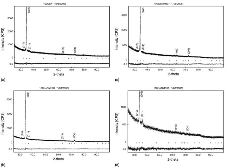
FIG. 1. Rietveld graphics for different compositions of Ga1−xMnxN films关共a兲–共d兲兴deposited by reactive sputtering. Each figure关共a兲–共d兲兴shows the observed
pattern共dot line兲, calculated pattern共solid line兲, and the goodness of the fit or residual pattern共at the bottom兲, obtained from the difference between calculated and observed patterns. The corresponding refinement results are presented in TableI.
063526-2 Dias da Silvaet al. J. Appl. Phys.102, 063526共2007兲
strong preferential orientation at the 关002兴 direction. Using the Scherer formula and the diffraction peak width, we could estimate crystallite mean sizes of the order of 25 nm in all samples.
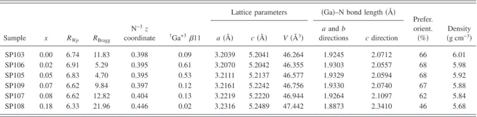
The data obtained by Rietveld refinement are shown in Table I. The preferential orientation parameter in the 关002兴
direction, associated with thecaxis perpendicular to the sub-strate surface, was calculated using the March-Dollase func-tion. The data show that the samples with lower manganese concentrations共up tox⬍0.07兲display higher degree of ori-entation, reaching approximately 68% in sample SP106. For higher Mn concentrations 共x⬎0.08, Table I兲 the orientation degree decreases, indicating that higher amounts of manga-nese tend to break the long range ordering incdirection.
The lattice expansion caused by the manganese inser-tion, noticed by the increase of the unit cell volume from 46.264 共GaN兲 to 47.442 Å3 共x= 0 . 18兲, can be associated with the bigger size of the manganese as compared to gal-lium. This fact, associated with the smaller atomic weight of
Mn 共54.94 g mol−1兲 compared with that of Ga
共69.72 g mol−1兲, causes also the decrease in the material den-sity from 6.01共GaN兲to 5.68 g cm−3 共x= 0.18兲. The increase in the unit cell volume as a consequence of the Mn insertion occurs almost isotropically with the a andcparameters in-creasing simultaneously. As a matter of fact, the ionic共 cova-lent兲 radii of Ga+3, Mn+3, and N−3 in angstroms are 0.47
共0.61兲, 0.58 共0.72兲, and 1.46共1.32兲, respectively,23 thus the expected ionic and covalent Ga–N bond lengths for this structure are both 1.93 Å. It is interesting to notice that in spite of the monotonic increase in the lattice parameters共a
=b andc兲, the bond distances displayed in TableIexhibit a slightly different behavior. In a and b directions, the bond distance suffers firstly a slight increase共for smallx兲and later tends to decrease with the increase in the Mn content, being of the order of the sum of the covalent radii. On the other hand, the bond incdirection that is of order of the sum of the ionic radii presents a slight decrease with the first Mn incor-poration and then increases continuously with the Mn con-tent. The bond polarities and lengths that take place in this structure should play an important role in defining the pref-erential orientation texture observed in the films.
The nitrogen position共N−3zcoordinate, TableI兲remains practically unaffected until x= 0.07, showing that the
struc-ture expands isotropically to receive low concentrations of the Mn cation in the Ga site. When the Mn concentration is further increased from this value, the nitrogen atoms leave their original positions, affecting also the rigid positions of the gallium site. This effect can be observed by the increas-ing in the RBraggfactor, which is associated with correlation between the real structure with the proposed model. In spite of this, a good refinement quality was obtained for all of the samples, noticed by the Rwp factor, which presents values between 6% and 7%.
The thermal anisotropic parameter for the Ga sites共11兲
should be interpreted in association with the variations of the nitrogen coordinate 共N−3z兲 and the lattice parameters. The biggest oscillation of this parameter, corresponding to the oscillations of the Ga and Mn ions in the referred direction for the x= 0.02 andx= 0.05, can be understood as a conse-quence of the insertion of Mn in the lattice, since in these samples, the lattice expansion is not followed by the dis-placement of the N atom. As a consequence the cation sites are expanded raising the diffraction probability of these sites. With the increase of the Mn concentration abovex= 0.05 the nitrogen atoms are displaced toward z= 0.5, demonstrating that the higher amounts of manganese require more space. This structural rearrangement comprises the gallium site in theab plane, noticed by the decrease in the11 values. On the other hand, an increase in c is verified, causing the in-crease in Ga–N bond length. This event leads to the enhance-ment ionic character of the bond in the c direction, which is followed by the decrease of the preferential orientation of the crystallites.
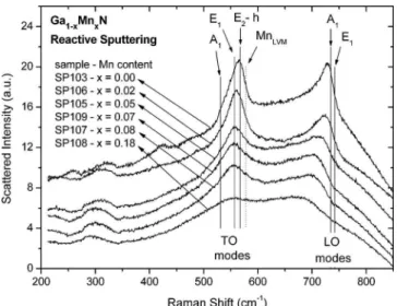
The vibrational properties of the films were focused with
the help of Figs. 2 and 3, which display the micro-Raman
and infrared absorption results, respectively. Figure2shows the first order Raman scattering bands for films with different Mn contents. The peak positions corresponding to the trans-verse and longitudinal optical modes in the GaN bulk crys-tals are indicated by vertical lines. The dotted line in 578.5 cm−1 represents the vibrational frequency of a local-ized mode associated with the Mn,7,8,24 which will be dis-cussed ahead. A band associated with the acoustic modes of disordered GaN is also observed in 300 cm−1.10,12,19
As it was expected for nanocrystalline films, the Raman spectra of the undoped material共x= 0兲presents intermediate
TABLE I. Refined structural data for Ga1−xMnxN films with different Mn contents obtained through the Rietveld refinement. Structure: hexagonalP63mc 共C6v
4兲,Z= 2,共Ref. ICSD: 25-676兲, Atomic positions: Ga+3共1 / 3 , 2 / 3 ; 0兲, Mn+3共1 / 3 , 2 / 3 ; 0兲, N−3共1 / 3 , 2 / 3 ;z兲, whereR
Wpis the refinement quality parameter,
RBraggis the structural conformity parameter, and11 is the anisotropic displacement parameter. Lattice and bond parameters are also displayed, as well as the
preferential orientation and density.
Sample x RWp RBragg
N−3z
coordinate †Ga+311
Lattice parameters 共Ga兲–N bond length共Å兲
Prefer. orient.
共%兲
Density
共g cm−3兲 a共Å兲 c共Å兲 V共Å3兲
aandb
directions cdirection
SP103 0.00 6.74 11.83 0.398 0.09 3.2039 5.2041 46.264 1.9245 2.0712 66 6.01
SP106 0.02 6.91 5.29 0.395 0.61 3.2070 5.2042 46.355 1.9303 2.0557 68 5.98
SP105 0.05 6.83 4.70 0.395 0.53 3.2111 5.2137 46.577 1.9329 2.0594 68 5.92
SP109 0.07 6.62 9.84 0.397 0.12 3.2161 5.2242 46.756 1.9330 2.0740 67 5.88
SP107 0.08 6.62 12.82 0.404 0.13 3.2219 5.2220 46.944 1.9264 2.1097 62 5.84
SP108 0.18 6.33 21.96 0.446 0.02 3.2316 5.2489 47.442 1.8873 2.3410 46 5.68
063526-3 Dias da Silvaet al. J. Appl. Phys.102, 063526共2007兲
characteristics between the GaN crystal19 and the spectrum of the corresponding amorphous20 material. The bands asso-ciated with the sets of convoluted TO and LO modes are clear in the undoped sample, being the signal measured in the backscattering configuration without polarization. The observed bands are considerably broader and the component modes are not resolved, as compared to the observed in the GaN and Ga1−xMnxN bulk crystals: the reported LO-A1
共TO-E2-high兲peak width is⬃6 cm−1共Ref.25兲 关12 cm−1共Ref.
19兲兴, while in our samples the width of the LO共TO兲band is approximately 32 cm−1 共30 cm−1兲. In amorphous GaN with similar excitation共458 nm兲, the optical modes show up in a single band, with approximate width of 160 cm−1, in which it is not possible to deconvolute the TO and LO bands.20In the amorphous case only a slight structure is observed in the broad optical band, and a clear raise in the scattering is ob-served at frequencies below 350 cm−1in association with the acoustic modes.20
The broadening of the optical vibrational peaks in our spectra can be explained by the partial relaxing of the selec-tion rules during scattering caused by the disorder of the lattice. In this way the scattering spectra also present the contribution of modes with wave vectors located outside the Brillouin zone center. Consistently, the shape of the spectrum of the nanocrystalline undoped sample resembles a broad-ened version of the vibrational mode density of states of the corresponding crystal26and with the density of states 共DOS兲
extracted from neutron diffraction experiments.27
The influence of Mn in the vibrational properties of the Ga1−xMnxN films was noticed through general aspects of the
changes produced in the spectrum, but no apparent specific band was found. The presence of Mn affects more inten-sively the band related to the LO modes due the anisotropic changes in the lattice parameters of the GaN structure caused by Mn insertion in the Ga site, which is consistent with the
strong increase in the 11 parameter for small x values
共TableI兲. Effectively, with the increase of the Mn concentra-tion, the shift of the LO peak to smaller frequencies, the weakening of its maximum intensity, and its broadening are
observed. Reported polarized measurements7 indicate that
the disorder component associated with the presence of Mn in this peak is strong even in monocrystalline films produced
by MBE.7
In a similar trend to the band related to the LO modes, the band associated with the TO modes displays a consider-able broadening 共full width at half maximum of⬃30 cm−1兲
when compared with measurements of particular vibrational modes reported for GaN crystals.7,19Also, if one considers the frequency superposition between this band and the crys-tal TO modes共Fig.2兲, it can be concluded that the observed band corresponds to an overlapping of the E1, E2, and A1
modes. TheA1is not allowed in the crystal when the excita-tion is in thec-axis direction, but it can be present here by the effect of the disorder.
One component associated with a localized vibration mode共LVM兲of Mn is expected at high frequency vicinity of the TO-E2peak.7,8,24The frequency of this mode, valid in the limit of low Mn concentration, can be estimated using the effective mass approximation,7,8,24
Mn-LVM=GaNTO
冑
GaNMnN. 共1兲
The estimation of this frequency for bulk Ga1−xMnxN
共Ref. 8兲 and for films prepared by MBE共Ref. 7兲 gives the values of 574 and 586 cm−1, respectively, while the same approximation in our samples results in 578 cm−1共TableII兲. The broadening of the TO peak includes this frequency, even in the sample without Mn. In this way it is difficult to
indi-FIG. 2. Micro-Raman scattering spectra of Ga1−xMnxN films with different
Mn concentrations, measured at room temperature using the Ar+488.0 nm
laser line excitation. The spectra were vertically shifted for clarity. The vertical solid lines indicate the positions of zone-center phonons in wurtzite GaN crystals共Ref.19兲and the vertical dotted line is located at the calcu-lated Mn recalcu-lated impurity mode frequency共Ref.8兲.
FIG. 3. Fourier transform infrared spectra in the spectral range correspond-ing to the band related to the TO modes of GaN / GaMnN films. The posi-tions of the peaks are displayed in Fig.4. Different curves correspond to different Mn contents. Bands related to the substrate absorption can also be noted in 512 and 610 nm, corresponding, respectively, to lattice vibration and impurity absorption of the Si wafer.
063526-4 Dias da Silvaet al. J. Appl. Phys.102, 063526共2007兲
vidualize a band at this frequency in our spectra, even though the changes in the line shape with the increasing Mn content are consistent with the existence of such band. In this way we did not succeed in individualizing a component associ-ated with the localized Mn modes. Harima7observed that the detection with crossed polarization relative to the excitation in Ga1−xMnxN crystals promoted the individualization of a
peak in 586 cm−1, and consequently associated its presence with the TO-E2-high mode associated with the vibrations of Mn in Ga sites, which are known to presentC3vsymmetry in the wurtzite lattice.
The TO-A1 mode of the GaN–GaMnN is IR active, and
Fig.3shows the absorption bands in FTIR spectra associated with this mode. The minimum of the transmittance spectrum
共maximum of the absorption coefficient兲 tends to shift to lower frequencies to broaden and to increase the maximum absorption with the Mn content increase. The absorption in-crease and the shift observed are probably directly associated with the increase in polarity of the cation-N bonds in thec
direction as function of Mn content, which was determined through the increase in the bond length values incdirection by the Rietveld method.
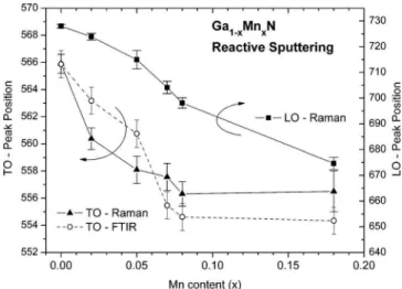
Either in IR absorption band maximum or in the Raman scattering peak, it is possible to notice that the frequency of the TO bands tends to be shifted to smaller frequencies with the increase of the Mn content, Fig.4. Nevertheless, the am-plitude of the shift is smaller in this case as compared with
the observed shifting in the LO peak, as can be seen through the analysis of Fig.4and TableII. Concerning the TO mode, the shift occurs in the range limited by the TO-E2-high and TO-E1modes of the spectrum of the GaN crystal.
With the increase in the Mn content, the scattered inten-sities between the LO and TO peaks become increasingly important. The spectrum line shape presents well defined LO and TO bands whenx= 0, but evolves to a structure in which these peaks are almost completely convoluted whenx= 0.18. A similar behavior was reported for Ga1−xMnxN films with
high Mn content and high disorder degree,7,10 and can be understood, in general, as a result of disorder. In particular, the increases of both the N vacancies 共dominant兲and of the
MnLVM peak component 共minoritary兲 are expected to
con-tribute to the scattering in the frequencies between the TO and LO peaks.
We could not notice in the spectra any characteristics directly related to the free carriers or to the interaction
be-tween carriers and vibrational modes. In n doped GaN the
interaction with plasmons was reported to cause an important coupling with the LO modes, producing a shift of the corre-sponding peak to high frequencies,19,28while thep doping is expected to cause an increase in the scattering at low frequencies.29
The shift of the transmittance minima to smaller fre-quencies is represented in Fig. 4 together with the shifts of the Raman peaks. There is a close similarity between the shifts observed in the transmittance, related to the TO-A1, mode and the Raman TO peak, which in our measurements is
probably dominated by theE2-high modes. Based on known
results for the Raman scattering in GaN共Ref.19兲and on the modifications in the line shape of the TO peak, we can speculate that for low Mn content and high orientation tex-ture in the direction perpendicular to the substrate, the Ra-man TO band is dominated by theE2-highmodes. Differently, when the Mn concentration is high and the orientation tex-ture becomes weaker, it is probable that the Raman TO-A1
andE1, which have smaller frequencies, are raised, while the
E2-highpeak tends to decrease, since it is dependent on the
alignment between the caxis and the incident beam normal
to the substrate. Besides the decrease of the overall Raman scattering and the increase of the IR absorption are probably related to the increase of the polar character of the material bonds observed in the Rietveld analysis.
The disorder effect produced by the Mn insertion in Ga site is observed through the increase in the anisotropic dis-placement parameter for the Ga-site atoms 共11兲, which is followed by a decrease in the film orientation texture. This result is consistent with the vibrational band broadening, red-shifts, and the presence of acoustic bands. These lattice dis-order effects can affect the magnetic properties of the mate-rial by changing carrier dynamics characteristics and consequently the interaction of carries with localized mag-netic moments of the Mn ions with the lattice neighboring atoms.
Both the x-ray diffraction and the Raman scattering do not show any evidence of phase segregation, indicating that if there are segregated clusters, their occurrence is below the detection limit of these techniques. In the scanning electron
TABLE II. Wave numbers of values of the Raman bands maxima and FTIR minima for Ga1−xMnxN samples with different Mn contents.
Sample x
Raman TO Raman LO FTIR TO
共cm−1兲 共cm−1兲 共cm−1兲
SP103 0.00 565.9 728.0 565.7
SP106 0.02 560.4 723.9 563.2
SP105 0.05 558.1 715.0 560.7
SP109 0.07 557.6 704.1 555.5
SP107 0.08 556.3 698.1 554.6
SP108 0.18 556.5 674.6 554.3
FIG. 4. Peak position related to the TO 共left axis兲 and LO 共right axis兲
vibration modes of Ga1−xMnxN compound, as determined by Raman and
FTIR data共TO兲.
063526-5 Dias da Silvaet al. J. Appl. Phys.102, 063526共2007兲
microscopy measurements we did not find composition dif-ferences in film surfaces with different superficial morpholo-gies. The homogeneity of the samples is also evidenced in the micro-Raman spectra taken in different positions and in the regularity of the transmittance spectra in the visible and near infrared ranges.15 Thus, we can conclude that in the films prepared by reactive sputtering under the conditions used, the cluster formation or phase segregation is absent or very small, that is, the produced material is essentially ho-mogenous. In this way the Ga1−xMnxN nanocrystalline films
produced by reactive sputtering are potential candidates to present interesting properties, such as ferromagnetism at temperatures above 300 K, in spite of the observed disorder effects. The magnetic characterization of the material will be addressed in a future work.
IV. CONCLUSIONS
The structural and vibrational properties of nanocrystal-line Ga1−xMnxN films prepared by reactive cosputtering were
analyzed in a wide composition range. A strong orientation texture in which the c axis of the wurtzite crystallites ori-ented perpendicular to the substrate surface is present in the material. With the progressive Mn incorporation, an increase in the bond length and in the ionic character of the cation-N
bond along the c axis are observed. Correspondingly, the
vibrational frequencies of the bands associated with the set of TO and LO modes decrease with the increase of the Mn content, indicating a weakening of the cation-N bond and an increase of the lattice disorder.
Through the structural refinement and spectroscopic techniques, it was shown that the vibrational changes origi-nated from the Mn insertion in Ga site occur in a progressive way, while the structural changes do not. However, the com-bination of the results provide a clear mechanism to under-stand the modification in the structure of this material. The results indicate that the films do not display phase segrega-tion and that the Mn substitusegrega-tionally occupies the Ga sites in wurtzite crystallites. The obtained results are consistent with single phase nanocrystalline material.
ACKNOWLEDGMENTS
We would like to acknowledge the FAPESP agency
共Grant Nos. 2005/02249-0, 2004/12120-1, and 2006/
05627-8兲 for the financing, Professor Margarida Juri Saeki
for the use of the FTIR equipment, and L. F. da Silva for the assistance with the x-ray diffraction measurements.
1T. Dietl, H. Ohno, F. Matsukura, J. Cibert, and D. Ferrand, Science287,
1019共2000兲.
2S. J. Pearton
et al., J. Appl. Phys.93, 1共2003兲.
3S. Kuwabara, T. Kondo, T. Chikyow, R. Ahmet, and H. Munekata, Jpn. J.
Appl. Phys., Part 240, L724共2001兲.
4M. E. Overberg, C. R. Abernathy, S. J. Pearton, N. A. Theodoropoulou, K.
T. McCarthy, and A. F. Hebard, Appl. Phys. Lett.79, 1312共2001兲.
5G. Thaler, R. Frazier, B. Gila, C. R. Albernathy, S. J. Pearton, and C.
Segre, Appl. Phys. Lett.84, 1314共2004兲.
6S. Sonoda, S. Shimizu, T. Sasaki, Y. Yamamoto, and H. Hori, J. Cryst.
Growth37–239, 1358共2002兲.
7H. Harima, J. Phys.: Condens. Matter14, R967共2002兲.
8W. Gebiki, J. Strzeszewski, G. Kamler, T. Szyszko, and S. Podsiadlo,
Appl. Phys. Lett.76, 3870共2000兲.
9M. Zajac
et al., Appl. Phys. Lett.78, 1276共2001兲.
10Y. Y. Yuet al., J. Cryst. Growth269, 270 共2004兲.
11L. L. Guo, H. Zhang, and W. Z. Shen, Appl. Phys. Lett. 89, 161920 共2006兲.
12Y. H. Zhang, L. L. Guo, and W. Z. Shen, Mater. Sci. Eng., B130, 269 共2006兲.
13S. Granville
et al., J. Appl. Phys.100, 084310共2006兲.
14Y. K. Byeun, K. S. Han, H. J. Choi, and S. C. Choi, Mater. Sci. Eng., A, 452–453, 499共2007兲.
15D. M. G. Leite, L. F. da Silva, A. L. J. Pereira, and J. H. Dias da Silva, J.
Cryst. Growth294, 309共2006兲.
16Q. X. Guo, A. Okada, H. Kidera, T. Tanaka, M. Nishio, and H. Ogawa, J.
Cryst. Growth237, 1079共2002兲.
17M. Marques, L. K. Teles, L. M. R. Scolfaro, J. Furthmüller, F. Bechstedt,
and L. G. Ferreira, Appl. Phys. Lett.86, 164105共2005兲.
18I. T. Yoon, T. W. Kanga, and D. J. Kimb, Mater. Sci. Eng., B134, 49 共2006兲.
19N. E. Christensen and P. Perlin, inSemiconductors and Semimetals, edited
by R. K. Willardson and E. R. Weber共Academic, New York, 1998兲, Vol. 50, Chap. 13, pp. 409–427.
20H. J. Trodahl, F. Budde, B. J. Ruck, S. Granville, A. Koo, and A. Bittar, J.
Appl. Phys.97, 084309共2005兲.
21D. M. G. Leite, A. L. J. Pereira, L. F. da Silva, and J. H. Dias da Silva,
Braz. J. Phys.36, 978共2006兲.
22R. A. Young, A. C. Larson, and C. O. Paiva-Santos, User’s Guide to Program DBWS-9807 for Rietveld Analysis共Georgia Institute of Technol-ogy, Atlanta, 1998兲.
23R. D. Shannon, Acta Crystallogr., Sect. A: Cryst. Phys., Diffr., Theor. Gen.
Crystallogr.32, 751共1976兲.
24A. Kaschneret al., Appl. Phys. Lett.74, 3281共1999兲.
25L. Shi, F. A. Ponce, and J. Menendez, Appl. Phys. Lett.34, 3471共2004兲. 26C. Bungaro, K. Rapcewicz, and J. Bernholc, Phys. Rev. B 61, 6720
共2000兲.
27J. C. Nipko, C. K. Loong, C. M. Balkas, and R. F. Davis, Appl. Phys. Lett. 73, 34共1998兲.
28H. Harima, H. Sakashita, T. Inoue, and S. Nakashima, J. Cryst. Growth 189/190, 672共1998兲.
29H. Harima, T. Inoue, S. Nakashima, K. Furukawa, and M. Taneya, Appl.
Phys. Lett.73, 2000共1998兲.
063526-6 Dias da Silvaet al. J. Appl. Phys.102, 063526共2007兲