Test Structure for L1 Cache in Tiled CMPs
Mousumi Saha, Biplab K Sikdar
Abstract—This work reports a test structure to decide on the correctness of cache performance in chip multiprocessors (CMPs). The design targets the private L1 cache existing in Tiled CMPs architecture. It is developed around the cellular automata (CA) structure proposed by von Neumann in 1950’s. The theory of 3-neighborhood null-boundary CA is developed to record the inconsistent behavior of each of the processors L1 caches in CMPs. The special class of single length cycle attractor cellular automata accepts the (March) read/write status of cache word/line and evaluates the decision on the defective/inaccurate functioning of a cache module. This overcomes the inability of the classical design to identify defective behavior of CMPs cache. The test design further enables identification of the region of defective cache module in the CMPs that can help designers for defect diagnosis at design phase.
Index Terms—CMPs, cache testing, cellular automata, SACA, TACA, March test
I. INTRODUCTION
Chip Multiprocessors (CMPs) have been widely adopted [1] [2] [3] [4] [5] as the building block for future com-puter systems. Instead of building highly complex, power-hungry, single-threaded processors, CMP designers integrate multiple, potentially simpler, processor cores on a single chip to improve the overall throughput while reducing power consumption and design complexity [6] [7]. As the number of processor cores increases [8], a key aspect of CMP design is to provide fast data access for on-chip computation resources. However, the increasing number of cores in CMPs adds threats on reliability and dependability of a design. Efficient solutions are, therefore, demanded to overcome the non-compliance of the existing solutions designed for the single processor chip. A number of works has addressed the issue from different perspectives [9] [10] [11] [12] [13].
Testing is effective in modern microprocessors to detect both latent hardware defect and new defects appearing in logic and memory modules. In multithreaded multicore pro-cessors, caches are organized in multiple levels and multi-bank architectures that occupy almost 90% of the relative chip area. An innovative solution, therefore, is to be framed to find more accurate solution to the problem [14].
In 80s, Wolfram [15] studied a family of simple 1-dimensional cellular automata (CA) that could simulate complex system behaviors. A special class of Wolfram’s 3-neighborhood CA, called the linear/additive CA had been employed for developing effective methodologies for VLSI design [16]. The CA had also been found effective for efficient design of fault detection and diagnosis schemes in VLSI circuits [17][18][19].
Manuscript received September 25, 2015; revised December 30, 2015. Mousumi Saha is with the Department of Computer Applications, Na-tional Institute of Technology, Durgapur, India, [email protected].
Biplab K Sikdar is with the Department of Computer Science and Tech-nology, Indian Institute of Engineering Science and TechTech-nology, Shibpur, India, [email protected]
A cellular automata (CA) based realization of March algorithm for testing memories is reported in [20] to avoid bit by bit comparison of memory words, required in the conventional test designs. It is found to be superior than that reported in [21]. This provides the basis of this work that address the issue of high speed decision on the cache performence in CA framework.
In this background, this work targets solution for taking decision on the cache behavior to enable high performance / uninterrupted computation in CMPs. We consider 3-neighbo-rhood CA, to develop such a solution for the CMPs caches. The CA defined in 3-neighborhood runs on the status read from each cache word/line of the processors L1 caches and computes the behavior of the cells (defective or not) of an L1 cache module. It memorizes any defect in cache word during a run of March algorithm. The specific state of the n-cell CA, indicates the defective behavior (if any) of cache module. This further enables identification of the region of defective cache module in CMPs that can provide an effective solution for design defect diagnosis.
So, the salient features of this work are as follow:
• This basic design has been used in 3-neighborhood CA for fault detection of CMPs L1 cache to avoid bit by bit comparison of cache memory words, required in the conventional test designs.
• The test design also enables identification of the region of defective cache module in the CMPs and memorizes the fault along with self-testing approach.
• The study and work on testing the cache module of CMPs architecture based on 3-neighbourhood CA revealed that two instead of four rules [22] can be conveniently applied to memorize and disgnose the fault.
• In formulating Rule 252 and 255, further studies leading to theorems, experiments and results, had to be carried out.
The regular structure of CA suits better for low cost VLSI implementation of the test logic. The CA based test hardware for testing cache performance is introduced in Section IV. Section III reports the design detail. The next section provides CA preliminaries relevant to the current work.
II. CELLULARAUTOMATA
A Cellular Automaton (CA) is an autonomous finite state machine that evolves in discrete space and time. Each cell stores a discrete variable at timet that refers to the present state (PS). The next state (NS) of the cell at(t+1)is affected by its state and the states of itsneighborsatt. In this work, we consider the 1-dimensional CA, where a cell is having two states - 0 or 1 and the next state of ith
TABLE I
RM TS OF THECA <116,222,252,254,255>
PS 111 110 101 100 011 010 001 000 Rule Logicalf unction
RM T (7) (6) (5) (4) (3) (2) (1) (0)
NS 0 1 1 1 0 1 0 0 116 f =SiS
′
i+1+Si−1S
′
i
NS 1 1 0 1 1 1 1 0 222 f =Si+S
′
i−1S
′
i+1+Si+1
NS 1 1 1 1 1 1 0 0 252 f =Si−1+Si
NS 1 1 1 1 1 1 1 0 254 f =Si−1+Si+Si+1
NS 1 1 1 1 1 1 1 1 255 f = 1
0 1
00 Si−1
Si Si+1
01 11 10
1 1 Rule 255 1 1 1 1 1 1
f = 1
0 1
00 Si−1
Si Si+1
01 11 10
1
1 1 1
Rule 252
1
0 1
0
f = S + S
i+1 i
Fig. 1. Next state function for rule 252 and 255
Sit+1=fi(S t i−1, S
t i, S
t i+1) St
i−1,S t i andS
t
i+1 are the present states of the left neigh-bor, self and right neighbor of the ith
cell at time t and fi is the next state function. The states of the cells St
= (St 1, S
t 2,· · ·, S
t
n) at t is the present state of the CA. Therefore, the next state of ann−cellCAis
St+1= (
f1(S
t
0, S
t
1, S
t
2), f2(S
t
1, S
t
2, S
t
3),· · ·, fn(S t n−1, S
t n, S
t n+1))
The next state function of theith
CA cell can be expressed in the form of a truth table (Table I). The decimal equivalent of the 8 outputs (NSs) is called ‘rule’ Ri. In a 2-state 3-neighborhood CA, there can be 28
(256) rules. Five such rules 116, 222, 252, 254 and 255 are illustrated in Table I. The first row shows the combinations of PSs of (i−1)th
, ith
and(i+ 1)th
cells att. The last three rows list the NSs ofith
cell at (t + 1). A combinationSt i−1, S
t i, S
t
i+1 of PSi is referred to as the rule minterm (RMT). The column 011 of Table I is the 3rd RMT. The next states corresponding to this RMT are 0 for rule 51, and 1 for 254 & 255.
The 1-dimentional CA can be viewed as an array of cells where each cell configures with a rule. For an n-cell CA (n number of cells involved in CA), the rules that configure the cells form the rule vector. Rules of rule vcector of a CA may be uniform (all are same) or hybrid (nonuniform). The 3-cell CA with rule 254 can be written as CA<254, 254, 254>. The 4-cell CA with rule 250, 252, 254 and 255 can be written as CA<250, 252, 254, 255>, where the first cell (/leftmost cell) is set with 250, the second cell with 252, the third cell with 254 and the fourth cell with 255. The CA described first is uniform and the latter one is hybrid.
The left neighbour of the left most cell and right neighbour of the right most cell are considered zeros which are called null boundaries. In periodic boundary, the left neighbour of the leftmost cell is the rightmost cell and the right neighbour of the rightmost cell is the leftmost cell. Thus, it is formed into circular array.
1 3 7 5 13 9 11 2 6 4 12 8 14 15 10 0
Fig. 2. State transition diagram of CA<116,116,116,116>
1 13 7 3 9 11
4 5 12 14 6 15
8 0
10 2
Fig. 3. State transition diagram of CA<117,117,117,117>
State transition diagram(STD):State transition diagram of a CA describes the nature of its transition of states with time. The diagram shows that the CA goes from one state to another state with discrete time depending on the present state of the cell itself and states of its left neighbour and right neighbour cells. Simultaneously the present states of all three cells follow the logic of rule applied to that cell (described in 4th row of Table I). The logic of the rule can be derived using Karnaugh Map (Figure 1). Thus, simultaneously the present states of neighbors and applied rule take the decision of next state for a cell of CA.
A set of states can form loop (cycle) in the state transition diagram of a CA (0→0 and 1→1 of Figure 2). These are the attractors of the CA. The maximum distance traversed to reach an attractor from any other state is the depth of the CA. In Figure 2, the depth of the CA is 5.
After analyzing the state transition diagram, the following phenomena are observed:
• Each graph of STD always have an attractor(/cycle). • Any graph of STD never has more than one cycle i.e.
one graph one cycle. STD of CA<116,116,116,116> (Figure 2) has two graphs with two cycles, 0→0 and 1→1.
• An attractor may involve a single node (1→1 of Figure 2) or multiple nodes (13→7→3→9→13 of Figure 3). The attractor described first is a single length cycle at-tractor and the the latter is a multilength cycle atat-tractor. • An STD of a CA may have only single length cycle attractor graph or multiple length cycle attractor graph or combination of single length cycle and multilength cycle attractor graphs.
• Any node may have many predecessors but always has a single successor, i.e. two or more paths from predecessors to that node may exist, but more than one path never exist from that node to any other nodes.
• No of attractors and its magnitude depend on the no of cells in CA.
The CA with single length cycle attractor (0→0 and 1→1 of Figure 2) is found to be effective for the current design. The next section reports the identification of CA rules that can form single length cycle attractor.
A. Single length cycle attractor CA rules
A CAsynthesized with arbitrary rules may result in one or more attractors with multi-length cycles (Figure 2). To find the CA rules, desired for the proposed design, we need to analyze the property of the RMTs of a rule since nature of a CA is directly related to the nature of its RMTs. The following definitions and theorems are introduced that help to reduce the search space to identify the rules that only form single length cyle attractor CA. An attractor involving single node is called sigle length cycle attractor. It is also known as the fixed point attractor.
Definition 1 (Passive RMT): An RMTrof a rule is pas-sive if at time (t+1) a CA cell remains in the same state as in timet(0 to 0 or 1 to 1) onr. From Table I it can be seen that the RMTs 0, 2, 3, 6, and 7 of rule 254 are passive.
Definition 2 (Active RMT): An RMTrof a rule is active if a CA cell flips its state (1 to 0 or 0 to 1) onr. From Table I, it can be seen that the RMTs 1, 4, and 5 of rule 254 (2nd row) are active.
Definition 3 (Fixed Point Attractor): An attractor involv-ing sinvolv-ingle node is called sigle length cycle attractor. It is also known as the fixed point attractor.
Observation:All the RMTs of an RMT sequence for a fixed point attractor state are passive.
Theorem1: If RMTs- 0, 1, 2 and 3 in any rule R are simultaneously active, then there exists no fixed point attractor for the given rule R.
Proof: For a null boundary CA, the next state of the 1st cell (the left-most cell) is determined by the bit 0 (left neighbour), cell 1 itself and cell 2 (right neighbour). The different combinations of bits for cell 1 and cell 2 at timet is given in Table II.
Thus for any CA state, the value of cell 1, in terms of RMT is one among 0, 1, 2 and 3. Suppose, all the RMTs 0, 1, 2 and 3 are active, then the value of 1st cell at time (t+1) will be the complement of the value at time t. As a result,
TABLE II
DIFFERENTRMTVALUES FOR CELL1
0 cell 1 cell 2 RMT
0 0 0 RMT 0
0 0 1 RMT 1
0 1 0 RMT 2
0 1 1 RMT 3
CA can not remain in the same state in the next time step. Hence no fixed point attractor can be formed.
Theorem2: If the RMTs 0, 2, 4 and 6 in any rule R are simultaneously active, then there exists no fixed point attractor for the given rule R.
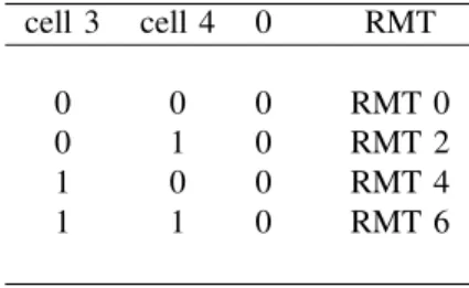
TABLE III
DIFFERENTRMTVALUES FOR CELL4
cell 3 cell 4 0 RMT
0 0 0 RMT 0
0 1 0 RMT 2
1 0 0 RMT 4
1 1 0 RMT 6
Proof: For a null boundary CA, the next state of the 1st cell (the left-most cell) is determined by cell 3, cell 4 and the bit 0 (right neighbour). The different combinations of bits for cell 3 and cell 4 at time t is given in Table III. Thus for any CA state, the value of cell 4, in terms of RMT is one among 0, 2, 4 and 6. Suppose, all the RMTs 0, 2, 4 and 6 are active, then the value of 4th
cell at time (t+1) will be the complement of the value at time t. As a result, CA can not remain in the same state in the next time step. Hence no fixed point attractor can be formed.
Theorem3: An even numbered CA rule can allow for-mation of at least one fixed point attractor, i.e. the state 0.
Proof:The 4-cell null boundary CA having one state of all 0s at time t, corresponds to RMT sequence sq<0,0,0,0>. For any even rule, RMT 0 is a passive RMT (next state 0 for RMT 0). Hence all the RMTs in the RMT sequence sq are simultaneously passive then CA would have next state of all 0s at time (t+1) and obviously it can form all 0s fixed point attractor, otherwise any one RMT in the RMT sequence sq is active it can not form all 0s attractor. Then CA can transit to another state at time (t+1).
Theorem4: If the RMTs 3, 6 and 7 of an even numbered CA rule are passive, it can allow formation of at least two fixed point attractors -that is, all 0s state and all 1s state.
TABLE IV
RULES GUIDING NON FORMATION OF FIXED POINT ATTRACTOR
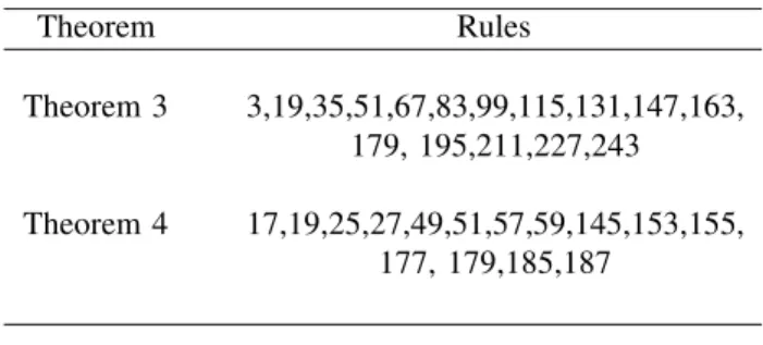
Theorem Rules
Theorem 3 3,19,35,51,67,83,99,115,131,147,163, 179, 195,211,227,243
Theorem 4 17,19,25,27,49,51,57,59,145,153,155, 177, 179,185,187
TABLE V
CARULES FOR SINGLE LENGTH CYCLE ATTRACTOR(UNIFORMCA)
number of Rule for single
passive RMTs length cycle attractor CA
3 2, 16, 32, 38, 52
4 0, 10, 15, 46, 106, 116, 120, 166, 174, 239, 244, 253, 254
all the RMTs in the RMT sequence sq are simultaneously passive then CA would have next state of all 1s at time (t+1). Obviously the even numbered rule with passive RMTs 3, 6 and 7 can allow formation of at least two fixed point attractors -that is, all 0s state and all 1s state.
Theorem 1 and 2 give a set of rules that can’t form fixed point attractors for a null boundary CA. These rules are given in Table IV. It must be noted that the table does not provide a complete set of rules that can’t form fixed point attractors. Since the reverse of the theorems 1 and 2, i.e., any of the RMTs 0, 1, 2 and 3 or RMTs 0, 2, 4 and 6 is passive and does not imply the existence of a fixed point attractor. However, Theorem 3 and Theorem 4 can help us to find the rules that can form single length cycle attractors (Table V).
Theorem5: An odd numbered CA rule can not allow formation of all 0s fixed point attractor.
Proof: Any odd numbered rule (for example 207, 145) has a 1 in the LSB (11001111 for rule 206). Thus the RMT 0 for an odd rule will always have the next state value 1. In other words, the RMT 0 for an odd rule is active. The state 0 corresponds to h0000i RMT sequence. Since the state 0 of an odd rule contains all active RMTs, hence state 0 can not allow a fixed point attractor for an odd rule of a null boundary CA.
Theorem6: If the RMTs 3, 6 and 7 are passive in an odd numbered CA rule, it can allow formation of at least one fixed point attractor -that is, all 1s state but it can not form an all 0s fixed point attractor.
Proof: The CA sinthesized with odd numbered ruleR can not allow to form all 0s fixed point attractor (Theorem 5), but if that rule R sumultaneously consists of passive RMTs 3, 6 and 7, then it can form a fixed point attractor of all 1s. So, the odd numbered rule with passive RMTs 3, 6, and 7 can allow formation of at least one fixed point attractor
TABLE VI
ATTRACTORS FOR RULES WHERE N(ATTRACTOR)=8
Rule Attractors
4 0,1,2,4,5,8,9,10 12 0,1,2,4,5,8,9,10 68 0,1,2,4,5,8,9,10 132 0,1,2,4,5,8,9,10 140 0,1,2,4,5,8,9,10 196 0,1,2,4,5,8,9,10 206 0,8,10,11,12,13,14,15 220 0,1,3,5,7,11,13,15
with all 1s state and can not allow formation of fixed point attractor with all 0s state.
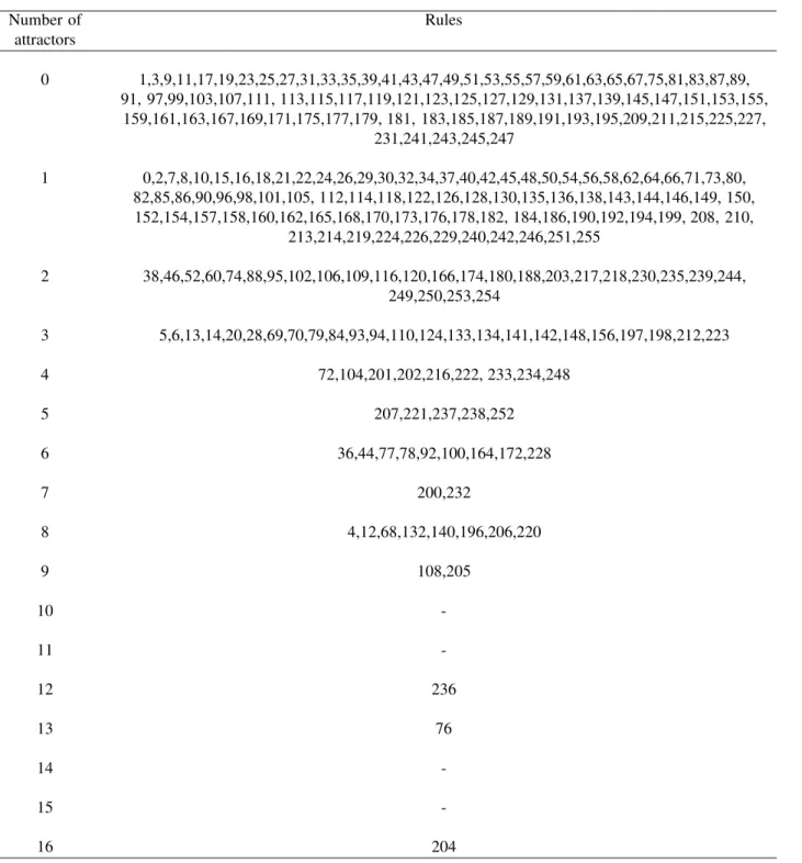
Table VI gives the 8-attractor rules and their magnitudes and Table VII provides a summary of all the rules for a 2-state 3-neighbourhood CA divided on the basis of the number of attractors. Column 1 of Table VII gives the number of attractors while column 2 contains their corresponding rules.
III. CACHE TESTING
A tiled CMP architecture consists of a number of repli-cated tiles connected over a switched direct network (Figure 4). Each tile contains a processing core with primary caches (both I- and D-caches), a slice of the L2 cache, and a connection to the on-chip network. The L2 cache is shared among the different processing cores, but it is physically distributed between them. Therefore, some accesses to the L2 cache will be sent to the local slice while the rest will be serviced by remote slices (L2 NUCA architecture). In addition, the L2 cache-tags store the directory information needed to ensure coherence between the L1 caches. On a L1 cache miss, a request is sent down to the appropriate tile where further protocol actions are initiated based on that blocks directory state.
In the design, we consider effective realization of March C− for determining correctness of the L1 cache function. However, any March algorithm, that is considered to be efficient in terms of fault coverage or any other parameter, can be realizable in the framework of proposed cellular automata (CA) based test hardware. A March test [23] [24] [25] [26] consists of a finite sequence of March elements. The March element is a finite set of operations applied to every cell in the cache array in sequence. An operation consists of writing a 0 (w0) into a cell Mi, reading an expected 0 (r0) from the cellMi; writing an 1 (w1) intoMi and then reading an expected 1 (r1) fromMi.
A read operation ‘r0’ or ‘r1’ of March algorithm stores then-bit word, read from the cache, to a register RG. These n bits are used to set the cell rules of an n-cell CA. The ith
-bit RGi sets rule for thei th
CA cell. If the CA is then run for some definite time steps, it settles to a state called attractor. For a fault in the cache, the least significant cell of the CA (Sigi) becomes ‘1’. On the other hand, Sigi is ‘0’ if the cache module is fault free. That is, by sensing only the Sigi, cache module can be declared as faulty or non-faulty.
TABLE VII
DIVISION OF RULES ON THE BASIS OF THE NUMBER OF ATTRACTORS
Number of Rules
attractors
0 1,3,9,11,17,19,23,25,27,31,33,35,39,41,43,47,49,51,53,55,57,59,61,63,65,67,75,81,83,87,89, 91, 97,99,103,107,111, 113,115,117,119,121,123,125,127,129,131,137,139,145,147,151,153,155,
159,161,163,167,169,171,175,177,179, 181, 183,185,187,189,191,193,195,209,211,215,225,227, 231,241,243,245,247
1 0,2,7,8,10,15,16,18,21,22,24,26,29,30,32,34,37,40,42,45,48,50,54,56,58,62,64,66,71,73,80, 82,85,86,90,96,98,101,105, 112,114,118,122,126,128,130,135,136,138,143,144,146,149, 150, 152,154,157,158,160,162,165,168,170,173,176,178,182, 184,186,190,192,194,199, 208, 210,
213,214,219,224,226,229,240,242,246,251,255
2 38,46,52,60,74,88,95,102,106,109,116,120,166,174,180,188,203,217,218,230,235,239,244, 249,250,253,254
3 5,6,13,14,20,28,69,70,79,84,93,94,110,124,133,134,141,142,148,156,197,198,212,223
4 72,104,201,202,216,222, 233,234,248
5 207,221,237,238,252
6 36,44,77,78,92,100,164,172,228
7 200,232
8 4,12,68,132,140,196,206,220
9 108,205
10
-11
-12 236
13 76
14
-15
-16 204
CPU Core Router L1 I Cache L1 D Cache
Directory
L2
Cache
Tile 1 Tile 2 Tile 3 Tile 4
Tile 5 Tile 6 Tile 7 Tile 8
Tile 9 Tile10 Tile11 Tile12
Tile13 Tile14 Tile15 Tile16
1 2 3 N
P 1 P 2 P 3 P
L1
N−cell CA
CA based
signature CA based signature
Decision
L1 L1 L1
CA based
signature CA based signature
Sig Sig Sig Sig
N
Fig. 5. Architecture of CA based test hardware for NUCA in CMPs
0
1
2
3
4
6
7 5
11
8 12
14
15 9
13
10
a) CA<252,252,252,252>
0
1 4
6
7
5 14
15 13
11 8
9
10
12
2
3
d) CA<252,252,255,252> 4
6
7 5 1
2
3 0
11
8 12
14
15 13
10 9
c) CA<252,255,252,252>
b) CA<255,252,252,252> 8
0
12
14
15 10
5 2
3
11 6
7
13 9 4
Fig. 6. State transition diagram of CA with fault free and faulty cache
That is, the signature response indicated in Figure 5 is tested with a CA as indicated in Figure 5. It checks the correctness of the signatures resulted out of N processors L1 caches. If signatures are found to be correct, it can be concluded that the cache module are working correctly. Otherwise, the output of the N-cell CA defines the region of defective cache module of the CMPs.
The design [22] has used the rule 254 and 255 to find the signature of the cache from the first stage since they can memorize the fault. We can not assign rule 192 and rule 207, since they can not memorize the fault. The sencond stage of the design [22] has used rule 192 and 207 to dignose the fault after getting all signature responses from the caches. In this stage, however, the rule 254 and rule 255 can not be used, since they do not have the diagnostic property. In our current work we have selected the rules 252 and 255 in both the stages because they are able to memorize as well as diagnose the fault. The next section reports the detailed design of the proposed test structure.
IV. TEST HARDWARE
The proposed test design employsn-cell CA that can settle to an single length cycle attractor X. Further, the best possible case can be, for fault free and faulty memory word, we need to form different CA so that the effect of fault can induce LSB of X as ‘1’ and ‘0’ for fault free.
In the example design of Figure 6(a) , the CA chosen for the fault free memory settles to an attractor 0 (all 0s state) if loaded with all 0s seed; in all other faulty cases, the CA selected settles to attractor 1 (withlsb1) (Figure 6(b)(c)(d)). That is, an incidence of fault in memory is translated as the switch from 0-basin to another basin withlsb1.
A. The CA structure
In this design (Figure 7) first stage activity is to test the cache performance and the second is to locate the fault region. The signature generated from the first stage gives forth the final decision in the second stage.
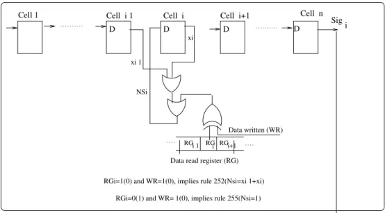
L1 cache module Sig
i i
D Q Cell N
Q D Cell 1
NSi
Data written (WR)
Cell i+1 D Q
Signature of ith Cell n
D Q
xi
xi−1
RGi−1 RG RGi+1
RGi=1(0) and WR=1(0), implies rule 252(Nsi=xi−1+xi) Data read register (RG)
RGi=0(1) and WR= 1(0), implies rule 255(Nsi=1) L1 cache module for Processor Pi (L1 )i
Cell 1
Decision
Sig i
Cell 2 D Q
i
Cell i
Q D Cell i−1
Q Q
D D
Cell i+1
Cell i Cell i−1
Q Q
D D
xi
xi−1
i
NSi
Sig
i
Sig =1; that is rule 255 (NSi =1) Sig =0; that is rule 252 (NSi =xi−1+xi)
Fig. 7. CA hardware test logic
the data bit read (r0) from cell Mi (RGi of Figure 7) is used to set the rule of ith
CA cell. The read bit RGi=0 is encoded as rule 252 ( WR=0, RGi=0 => NSi= xi−1 + xi i.e. NSi is equivalent to rule 252). When there is a fault in Mi, RGi=1 i.e. NSi=1. Therefore, rule 255 is set for thei
th cell (Figure 7).
On the other hand, when 1 is written (WR=1) to each cache cell Mi, the read bit RGi=1 is encoded as the rule 252 (WR=1, RGi=1 => NSi= xi−1 + xi -that is, NSi is equivalent to rule 252). For a fault in Mi, RGi=0 -i.e. NSi=1,rule 255 is set.
The activity of second stage is also similar to the first one. For an N no of L1 cache module, we employ anN-cell CA. When Signature is generated from ith L1 cache module (Sigi), it is used to set the rule of theith
CA cell. The Sigi=0
is encoded as the rule 252 (Figure 7) (Sigi=0=>NSi= xi−1 + xii.e. NSiis equivalent to rule 252). When there is a fault in cache module Sigi=1 i.e. NSi=1. Therefore, rule 255 is set for theith
CA cell (Figure 7).
Once signature is generated to all the cells, the CA is run
for t-steps (t <= N), initialized with all 0s seed. The CA for a fault free cache module is a uniform SACA constructed with rule 252 and so, it reaches the attractor state 0 (Figure 6(a)). On the other hand, for fault at one or more cells the CA is a hybrid one and it reaches a non-zero attractor with LSB=1 (Figure 6(b),(c) and (d)) after t-steps. Now, by sensing the LSB of the CA we can detect a faulty cache module.
V. PERFORMANCE ANALYSIS
The following discussion is to evaluate the performance of the test design in response to faults in the cache modules of CMPs.
A. Fault Detection and memorization
Let us consider the 5×4 cache memory of Figure 8 and assume that the 2nd
0 0 0 0 252 252 252 252 CA
CA 0 0 0 0 252 252 255 252
CA 252 252 252 252 252 252 252 252 CA
252 252 252 252 CA 0 0 0 0 252 252 252 252 CA
n=4 time steps For word 2: For word 1: For word 0:
For word 3: For word 4:
0 0 1 0 seed state state state
state
attractor 0 0 0 0
0 0 0 0 0 0 1 0 0 0 0 0 0 0 0 0 Word Memory
0 1 2 3
4 0 0 1 1 state
0 0 1 1 0 0 1 1
Fig. 8. Functioning of the test hardware for faulty cache
0s next state (Figure 6(a)). As word 1 is also fault free, the CA constructed for this is also the uniform CA with rule 252 and the next state is an all 0s state.
The operation ‘r0’ on word 2 results in a hybrid CA <252,252,255,252>. Its next state is non-zero 0010 (as per Figure 6(d), dotted box). The CA constructed on ‘r0’ of word 3 and 4 are also uniform CAs. Therefore, the CA for word 3 generates next state from 0010 to 0011 (3) and the CA for word 4 from 0011 to 0011 (3) (Figure 6(a)). The CA at word 4 is then run forn=4 steps and settles to the attractor state with least significant bit(lsb) 1 (Figure 8). Its lsb (1) defines that the memory is faulty. Figure 9 depicts that the cache is fault free.
That is, if thekth
(k < m) cache memory word is faulty, the test hardware [20] captures it as and only when the r0 [r1] is performed for thekth
word and memorizes it till the read operation on all the words are completed.
B. Fault diagnosis
The rule 252 and 255 applied in the first phase are to memorize the fault during performance measure of each cache module and the rules 252 and 255 applied in the second phase are to locate the region of faulty cache module during the analysis of signature. For instance, if thekth
cache module have a fault, the pattern will stuck to all 0s from msb to(k−1)th
position and all 1s fromkth toNth
position of the N-cell CA. The faulty L1 cache region can be located by analyzing the attractor state generated. For example, in Figure 6(c) the CA settles to the attractor 0111 (7) due to faulty signature from L1 of 2nd processor core. To identify the region of faulty L1 cache the N2
th
(that is, 2nd bit from left) of the attractor 0111 is checked. The bit is 1 implies that the fault is between 1st and 2ndcores. In a system with 16 processor cores (16 L1 caches), let say 5th cache produces faulty signature in stage 1. Then the stage 2 CA settles to an attractor 0000111111111111. To find the region of faulty L1 cache, the N2 = 8
th
bit of the attractor is to be checked. It is 1, which implies that the defective L1 is in between 1st
and 8th
cores. To find the exact region, we further need to check N
4 th
bit; it is zero in the present case and implies fault is in between N4
th and N8
th
cores. The similar steps continues with the bit position to be checked is 12N
th
. Therefore, the
identification of exact faulty region in worst case requires log N time steps.
C. Self testability
In the current design, we devise a technique to test the test hardware that can be tested without pushing additional logic. For this, the uniform CA with rule 252 in the first (second) phase of the test logic is initialized with 10000...0 seed. Then the CA is run forn-step (N-step) and settles to an attractor (all 1s for fault free test hradware, and for s-a-0 in test hardware the attractor with LSB 0). The LSB of the attractor then indicates faults in the test hardware.
D. Low hardware overhead
Apparently, by the analysis of CA, it seems that the component cost will increase but infact, our architecture place the CA on data path. So, considering the high density of memory, there will be no substantially increase in the entire chip area. It will be able to cater to varing and numerious demands. The overhead cost also be economically viable.
0 0 0 0
252 252 252 252 CA
0 0 0 0
252 252 252 252 CA
CA 252 252 252 252
252 252 252 252 CA
252 252 252 252 CA
CA 0 0 0 0 252 252 252 252
seed
n=4 time steps For word 2: For word 1: For word 0:
For word 3:
For word 4:
0 0 0 0 state
state
state
state
attractor 0 0 0 0
0 0 0 0
0 0 0 0
0 0 0 0
Word Memory
0 1 2 3
4 0 0 0 0 state
0 0 0 0
0 0 0 0 Cache
0 0 0 0
Signature/lsb=0
Fig. 9. Functioning of the test hardware for fault free
TABLE VIII PERFORMANCEEVALUATION
Test Hardware logic Capability of
Fault Detection Fault Memorization Fault Dignosis Self Testability
Ex-or logic Yes No No No
3-neighborhood rule 192/207 logic Yes No Yes Yes
3-neighborhood rule 254/255 logic Yes Yes No Yes
3-neighborhood rule 252/255 logic Yes Yes Yes Yes
the rule 252/255 logic to test, memorize and also diagnose the cache fault of CMPs (fourth row of Table VIII).
VI. CONCLUSION
This work proposes an efficient test structure for CMPs cache system. The solution is developed around the regular structure of 1-dimentional 2-state 3-neighborhood cellular automata (CA) with the target to achieve a self testing test structure. The special class of CA rules, forming single length cycle attractor CA, are chosen for the design. The logic, based on rule 252 and 255, is most suitable for our design compared to the rule 254/255 and 192/207 logic. The cellular automata have imense power to design an efficient circuit. The fault tolerant feature is posssible to be incorporated in the test design but the strategy for it has to be devised . To do this the rule, suitable for implementation in hardware circuit, has to be searched. This opens up future scope of work in CA based reliable test hardware design.
REFERENCES
[1] AMD. AMD Multi-core. http://multicore.amd.com/en/, 2006. [2] Intel. Multi-core from Intel. http://www.intel.com/multi-core/, 2006. [3] M. Gschwind, P. Hofstee, B. Flachs, M. Hopkins, Y. Watanabe, and T.
Yamazaki, ”A Novel SIMD Architecture for the Cell Heterogeneous Chip-multiprocessor” In Hot Chips 17, 2005.
[4] P. Kongetira, K. Aingaran, and K. Olukotun, ”Niagara: A 32-Way Multithreaded SPARC Processor.”IEEE Micro25(2):2129, 2005
[5] J. M. Tendler, J. S. Dodson, J. S. F. Jr., H. Le, B. Sinharoy, ”IBM Power4 System Microarchitecture.” IBM Journal of Research and
Development 46(1):526, 2002.
[6] Nontokozo P. Khanyile, Jules-Raymond Tapamo, and Erick Dube, ”An Analytic Model for Predicting the Performance of Distributed Applications on Multicore Clusters.” IAENG International Journal
of Computer Science, vol. 39, no. 3, pp 312-320, 2012.
[7] Tianyong Ao, Pan Chen, Zhangqing He, Kui Dai, Xuecheng Zou,
”RDCC: A New Metric for Processor Workload Characteristics Evaluation.”, IAENG International Journal of Computer Science,vol.
40, no. 4, pp 274-284, 2013.
[8] Intel. Tera-scale Computing. http://www.intel.com/technology/ techre-search/terascale/, 2006.
[9] Ransford Hyman, Koustav Bhattacharya, Nagarajan Ranganathan, ”Re-dundancy Mining for Soft Error Detection in Multicore Processors.”
IEEE Trans on Computers, Vol. 60, No. 8, August 2011.
[10] Pramod Subramanyan, Virendra Singh, Kewal K. Saluja, Erik Lars-son, ”Energy-Efficient Fault Tolerance in Chip Multiprocessors Using Critical Value Forwarding.”2010 IEEE/IIFIP International Conference
on Dependable Systems and Networks, 2010.
[11] Kunle Olukotun, Lance Hammond, ”The Future of Microprocessor.”
Magazine Queue - Multiprocessors, Vol 3 Issue 7, Pages 26-29,
September, 2005.
[12] Linzhi Ning, Wenbin Yao, Jun Ni, Nianmin Yao, ”Fault-Tolerant CMP Architecture Based on SMT Technology.” IEEE International
Multisymposium on Computer and Computational Sciences, 2007.
[13] Taotao Zhang, Ning Wu, Fang Zhou, Lei Zhou, and Xiaoqiang Zhang, ”A Traffic Equilibrium Mapping Method with Energy Minimization for 3D NoC-Bus Mesh Architecture.” IAENG International Journal of
Computer Science, vol. 42, no.1, pp. 1-7, 2015.
[14] Theodorou G, Kranitis N, Paschalis A and Gizopolos D, ”Software-based Self Test Methodology for On-Line Testing of L1 Caches in Multithreaded Multicore Architectures,” 2013 IEEE Transactions on
VLSI Systems, Vol. 21, No.4., 2013
[15] Wolfram S, Cellular Automata and Complexity – Collected Papers.
[16] Pal Chaudhuri P, Roy Chowdhury D, Nandi S, Chatterjee S, ”Additive Cellular Automata - Theory and Applications, volume 1’, IEEE
Computer Society Press, California,USA, ISBN 0-8186-7717-1, 1997.
[17] Hortencius P. D; McLeod R. D, Pries W, Card H. C., ”Cellular automata based pseudo-random number generators for built-in self-test.”
IEEE TCAD,8(8):842-859, August 1989.
[18] Sikdar, B. K, Ganguly, N, Chaudhuri P. P.’ ”Fault diagnosis of VLSI circuits with cellular automata based pattern classifier.” IEEE TCAD,
Vol: 24/7, pp. 1115 - 1131, 2005.
[19] Chattopadhyay S, Chowdhury D, Bhattacharjee S, Chaudhuri P. P., ”Cellular-automata-array-based diagnosis of board level faults”, IEEE TC., vol. 47/8, pp. 817-828, 1998.
[20] Saha M, Sikdar, B. K., ”High Speed Hardware for March C−”,ISED
2012,INDIA, 2012
[21] Baanen P., ”Testing word oriented embedded RAMs using built-in self test”,IEEE 1988.
[22] Saha M, Sikdar, B. K., ”An Efficient Method for Testing of L1 Cache Module in Tiled CMPs Architecture at Low Cost”, VLSI-SATA 2015, INDIA, 2015.
[23] A.J. van de Goor, ”Testing semiconductor memories, theory and practice”, John Wiley&Sons, Chichester, UK, 1991.
[24] Suk D. S, Reddy S. M., ”A march test for functional faults in semiconductor random access memories”, IEEE TC. vol: C-30, No. 12, pp. 982-985, December 1981.
[25] Said Hamdioui, Ad J. van de Goor, Mike Rodgers, ”March SS: A Test for All Static Simple RAM Faults”, Proceedings of the 2002 IEEE International Workshop on Memory Technology, Design and Testing (MTDT-2002).
[26] Swati Singh, UBS Chandrawat, ”Built-In-Self Test for Embedded Memories by Finite State Machine”, International Journal of Digital
Application Contemporary research,2013.
Mousumi Saha received the B.E degree in Computer Science and Engineering from the Regional Engineering College (Now National Institute of Technology), Durgapur in 1997 and M.Tech degree in CSE from Calcutta Univer-sity, West Bengal in 2001. She is currently working at National Institute of Technology, Durgapur as an Assistant professor in the department of Computer Applications. She is currently pursuing her PhD in the CSE depart-ment, Indian Institute of Engineering, Science and Technology, Shibpur, West Bengal. Her research interests include VLSI Design and Testing, Fault tolerant memory design, Theory of Cellular Automata and its application.