UNIVERSIDADE DO ALGARVE
INSTITUTO SUPERIOR DE ENGENHARIA
D
YNAMIC
P
OWER AND
F
REQUENCY
O
PTIMIZATION
IN
D
IGITAL
E
LECTRONIC
S
YSTEMS
O
PTIMIZAÇÃOD
INÂMICA DAT
ENSÃO DEA
LIMENTAÇÃO E DAF
REQUÊNCIA DEO
PERAÇÃO EMS
ISTEMASE
LECTRÓNICOSD
IGITAISAndré Azevedo de Sousa Romão
Dissertation for obtaining the Master degree in Electrical and Electronic Engineering
Specialization Area in Information Technologies and Telecommunications
Tutor: Professor Doutor Jorge Filipe Leal Costa Semião
September, 2013 ... DCO or DC-DC Global Sensor CUT V/F Controller Local Sensors
UNIVERSIDADE DO ALGARVE
INSTITUTO SUPERIOR DE ENGENHARIA
D
YNAMIC
P
OWER AND
F
REQUENCY
O
PTIMIZATION
IN
D
IGITAL
E
LECTRONIC
S
YSTEMS
O
PTIMIZAÇÃOD
INÂMICA DAT
ENSÃO DEA
LIMENTAÇÃO E DAF
REQUÊNCIA DEO
PERAÇÃO EMS
ISTEMASE
LECTRÓNICOSD
IGITAISAndré Azevedo de Sousa Romão
Dissertation for obtaining the Master degree in Electrical and Electronic Engineering
Specialization Area in Information Technologies and Telecommunications
Tutor: Professor Doutor Jorge Filipe Leal Costa Semião
Title: Dynamic Power and Frequency Optimization in Digital electronic Systems.
Authorship: André Azevedo de Sousa Romão.
I hereby declare to be the author of this original and unique work. Authors and references in use are properly cited in the text and are all listed in the reference section.
_________________________________ André Azevedo de Sousa Romão
Copyright © 2013. All rights reserved to André Azevedo de Sousa Romão. University of Algarve owns the perpetual, without geographical boundaries, right to archive and publicize this work through printed copies reproduced on paper or digital form, or by any other media currently known or hereafter invented, to promote it through scientific repositories and admit its copy and distribution for educational and research, non-commercial, purposes, as long as credit is given to the author and publisher.
Copyright © 2013. Todos os direitos reservados em nome de André Azevedo de Sousa Romão. A Universidade do Algarve tem o direito, perpétuo e sem limites geográficos, de arquivar e publicitar este trabalho através de exemplares impressos reproduzidos em papel ou de forma digital, ou por qualquer outro meio conhecido ou que venha a ser inventado, de o divulgar através de repositórios científicos e de admitir a sua cópia e distribuição com objectivos educacionais ou de investigação, não comerciais, desde que seja dado crédito ao autor e editor.
To my son David Romão and to my wife Raquel Romão, with love.
A
CKNOWLEDGMENTSFirst of all, I would like to thank to Dr. Jorge Semião, my tutor, for his personal and professional dedication, support and guidance in the elaboration of this dissertation. Without his help I would be completely lost, because the research area was new to me. He shared his knowledge, expertise and time, and that allowed me to finish this task.
To my wife Raquel Romão, who always believed in me and for all the help she provided. I love you and our son David Romão.
To my father Joaquim Romão and my mother Teodolinda Azevedo, that gave me good advices, on my personal, academic and professional and encouraged me to pursue this goal.
I also like to thanks to all my friends for the good break times that allow me to refill the energies and to fulfill this thesis.
Thank you all.
A
BSTRACTThe work developed consists in a power or frequency optimization methodology, for long-term operation, using global and local performance sensors. The methodology allows circuits to be optimized dynamically, during their life-time, according with one of the two possible needs: (1) restrict power consumption, by reducing power-supply voltage to the minimum value that prevents errors from happening; or (2) optimize performance, by increasing operating frequency to the maximum limit that prevents errors’ occurrence.
The use of both global and local sensors allows an on-line performance monitoring with information from the critical elements in the circuit and being conscious with the dynamic evolution of different variables that affect performance (e.g., aging degradation, temperature and power-supply variations).
Global sensors are used to perform periodic on-line monitoring. Local sensors are used to keep global sensors tuned with circuit’s performance. Both are sensitive to PVTA (Process, power supply Voltage, Temperature and Aging) variations, or to any other parameter that may affect performance, and both can trigger the supply Voltage or Frequency on-line tuning, along product lifetime, preventing functional errors.
Global sensor provides a coarse performance evaluation, while local sensors provide a fine grain performance evaluation on the real functional circuit.
Additionally, a new Delay-Fault Correction Flip-flop (DFC-FF) was presented, to improve the existing local aging sensors, and to allow not only the prediction of errors but also their correction, under certain limits.
Methodology was demonstrated with HSPICE simulations.
KEYWORDS: Performance sensor, Dynamic Voltage Frequency Scaling (DVFS),
Frequency and Power optimization, Aging prediction, Error-Correction.
R
ESUMOÀ medida que a tecnologia de circuitos integrados CMOS é exposta à miniaturização, surgem diversos problemas no que diz respeito à fiabilidade e performance. Efeitos tais como o BTI (Bias Thermal Instability), TDDB (Time Dependent Dielectric Breakdown), HCI (Hot Carrier Injection), EM (Electromigration) degradam os parâmetros físicos dos transístores CMOS e por sua vez alteram as propriedades eléctricas dos mesmos ao longo do tempo. Esta deterioração é chamada de envelhecimento e estes efeitos são cumulativos e têm um grande impacto na performance do circuito, especialmente se ocorrerem outras variações paramétricas, como as variações de processo, temperatura e tensão de alimentação. Estas variações são conhecidas por variações PVTA (variações no Processo de Fabricação do circuito integrado [P], na Tensão de Alimentação [V], na Temperatura [T] e variações provocadas pelo Envelhecimento dos circuitos [A]) e podem desencadear erros de sincronismo durante a vida do produto (circuito integrado digital).
O trabalho apresentado nesta dissertação tem por objectivo primordial o desenvolvimento de um sistema que optimize a operação ao longo da vida de circuitos integrados digitais síncronos de forma dinâmica. Este sistema permite que os circuitos sejam optimizados de acordo com as suas necessidades:
(i) Diminuir a dissipação de potência, por reduzir a tensão de alimentação para o valor mais baixo que garante a operação sem erros; ou
(ii) Aumentar o desempenho/performance, por aumentar a frequência de operação até ao limite máximo no qual não ocorrem erros.
A optimização dinâmica da operação ao longo da vida de circuitos integrados digitais síncronos é alcançada através de um controlador, um bloco de sensores globais e por vários sensores locais localizados em determinados flip-flops do circuito.
A nova solução tem como objectivo utilizar os dois tipos de sensores atrás mencionados, globais e locais, para possibilitar a previsão de erros de performance de uma forma mais eficaz, que possibilite a activação de mecanismos que impeçam a ocorrência de erros durante o tempo de vida útil de um circuito, e dessa forma
xiv
permitindo optimizar constantemente o seu funcionamento. Assim é exequível desenvolver circuitos que operem no limite das suas capacidades temporais, sem falhas, e com a utilização de margens de erro pequenas para admitir as variações de performance provocadas por variações no processo de fabrico, na tensão de alimentação, na temperatura ou o envelhecimento.
Foi também desenvolvido um sistema de controlo que permite, depois da detecção de um potencial erro, desencadear um processo para diminuir a frequência do sinal de relógio do sistema, ou aumentar a tensão de alimentação, evitando que o erro ocorra.
Apesar de existirem outras técnicas de controlo dinâmico da operação de circuitos integrados tais como DVS (Dynamic Voltage Scaling), de DFS (Dynamic Frequency Scaling), ou ambas (DVFS – Dynamic Voltage and Frequency Scaling), estas técnicas ou são de muito complexa implementação, ou apresentam margens de segurança elevadas, levando a soluções em que a operação do circuito não está optimizada. A solução desenvolvida neste trabalho, em que se utilizam sensores preditivos locais e globais os quais são sensíveis ao envelhecimento a longo prazo ocorrido nos circuitos, constitui uma novidade no estado da técnica relativamente ao controlo de sistemas de DVS e/ou DFS.
Outro aspecto importante é que neste trabalho desenvolveu-se um método de ajuste da tensão de alimentação ou da frequência, o qual é sensível ao envelhecimento a longo prazo dos circuitos, utilizando sensores locais e globais. O controlador permite a optimização da performance dos circuitos através do aumento da frequência de operação até ao limite máximo que ainda evita a ocorrência de erros e a optimização de consumo de energia através da redução da tensão de alimentação (VDD) para o valor mínimo que ainda previne a ocorrência de erros.
Através de uma análise de previsão de envelhecimento, são identificados os caminhos críticos, bem como os caminhos que envelhecem mais rápido e que se tornarão críticos com o envelhecimento do circuito. Uma vez identificados os caminhos críticos, irão ser inserido os sensores locais através da substituição dos flip-flops que terminam os caminhos críticos identificados por novos flip-flip-flops que incluem sensores de performance e de envelhecimento. É de referenciar que estes sensores são preditivos, ou seja, que sinalizam precocemente os erros de performance, antes de eles ocorrerem nos flip-flops que capturam os caminhos críticos. A arquitectura dos sensores propostos é tal que as variações PVTA que ocorrem sobre
eles fazem aumentar a sua capacidade de prever o erro, ou seja, os sensores vão-se adaptando ao longo da sua vida útil para aumentarem a sua sensibilidade.
Os sensores locais têm como função realizar a calibração dos sensores globais, bem como realizar a monitorização constante dos atrasos nos caminhos mais longos do circuito, sempre que estes são activados.
A função dos sensores globais é a realização da monitorização periódica ou quando solicitado dos atrasos no circuito digital. Ambos os tipos de sensores, os sensores globais como os locais podem desencadear ajustes na frequência ou na tensão de alimentação.
Os sensores globais são compostos por uma unidade de controlo do sensor global, que recebe ordens do controlador do sistema para iniciar a análise ao desempenho do circuito e gera os sinais de controlo para a operação de análise global do desempenho e por duas cadeias de portas (uma com portas NOR e outra com portas NAND), com tempos de propagação superiores aos caminhos críticos que se esperam vir a ter no circuito durante a sua vida útil. Ambos os caminhos irão, presumivelmente, envelhecer mais que os caminhos críticos do circuito quando sujeitos ao efeito BTI (que influencia fortemente a degradação do Vth dos transístores [NBTI/NORs e PBTI/NANDs]). Ao longo das duas cadeias, diversos sinais à saída de algumas portas NOR e NAND são ligados a células de sensores globais, criando diversos caminhos fictícios com diferentes tempos de propagação. As saídas dos sensores das duas cadeias formam duas saídas de dados do sensor global.
A fim de se alcançar a optimização do desempenho do circuito, são realizados testes de calibração dos sensores, onde são estimulados alguns caminhos críticos no circuito (através de um teste determinístico) e, simultaneamente é realizada a análise do desempenho pela unidade de sensores globais. Este procedimento, permite definir o limite máximo (mínimo) para frequência (tensão de alimentação) sem que os sensores locais sejam sinalizados. Esta informação da frequência (tensão) é guardada num registo do controlador (registo V/F) e corresponde à frequência (tensão) normal de funcionamento. Este teste também permite determinar quais os caminhos fictícios nas duas cadeias que apresentam tempos de propagação semelhantes aos caminhos críticos do circuito. Esta informação também é guardada em dois registos no controlador do sistema (registos GSOsafe), que indicam o estado das saídas dos controladores globais para a operação optimizada do circuito.
xvi
Durante a vida útil do circuito, o controlador do sistema de optimização procede ao ajuste automático da frequência (ou da tensão de alimentação) do circuito, caso o controlador dos sensores globais detecte uma alteração em relação à operação correcta em memória, alterando o conteúdo do registo que guarda a frequência (tensão) de trabalho.
Se por ventura ocorrer a sinalização de um sensor local e não existir nenhuma sinalização para alteração do desempenho pelos sensores globais, quer dizer que o circuito pode ter envelhecido mais que os caminhos fictícios dos sensores globais, pelo que a frequência (tensão de alimentação) de funcionamento deve ser alterada, mas também deve existir uma actualização nos registos que guardam a saída correcta dos sensores globais.
É de salientar que, se os caminhos fictícios envelhecem mais do que o circuito, as margens de segurança (time slack) existentes vão sendo aumentadas ao longo da vida do circuito, tratando-se de uma segurança positiva. Mas, se existir a possibilidade do envelhecimento ser maior nos caminhos do circuito, a existência dos sensores locais a monitorizar a todo o tempo o desempenho do circuito, garantem que o sistema pode aprender com as sinalizações e adaptar-se às novas condições de operação ao longo da vida útil do circuito.
Enquanto a monitorização efectuada pelo bloco de sensores globais fornece uma avaliação grosseira do estado de funcionamento do circuito, a monitorização efectuada pelos sensores locais, quando activados, fornece uma avaliação fina sobre qual a performance do circuito para que não ocorram erros funcionais.
As novidades apresentadas neste trabalho são no mecanismo de controlo que permite a optimização dinâmica da tensão ou da frequência, e na arquitectura e funcionamento do sensor global a inserir no circuito. No que diz respeito ao mecanismo de controlo do sistema de optimização dinâmica, as novidades são: (i) na utilização conjunta de sensores locais e globais para garantir níveis de optimização elevados, (ii) na utilização de sensores preditivos (globais e locais) que previnem os erros de ocorrerem e (iii) na utilização de sensores sensíveis ao envelhecimento do circuito ao longo da sua vida útil. Em relação ao sensor global para monitorização de variações PVTA a novidade consiste (iv), na apresentação de sensores para a degradação nos transístores PMOS e de sensores para a degradação nos transístores NMOS.
Este método de optimização e as topologias apresentadas podem ser desenvolvidas e utilizadas com outros tipos de flip-flops, ou empregando outros tipos de sensores, ou outros caminhos fictícios nos sensores globais, sem prejuízo do método global de optimização que conjuga os dois tipos de sensores, globais e locais, para optimizar a tensão de alimentação e a frequência de operação.
É proposta uma nova arquitectura para um flip-flop com correcção de erros de atraso (DFC-FF / AEPDFC-FF) com e sem previsão de erros adaptativa para realizar a correcção/monitorização e correcção on-line da perda de performance a longo prazo de sistemas digitais CMOS, independentemente da sua causa. O DFC-FF integra um FF do tipo TG-MSFF (Transmission Gate Master Slave Flip-Flop) e um sensor de correcção de erros (CES) dos quais são apresentados duas propostas. O AEPDFC-FF é composto por DFC-FF e um sensor de envelhecimento.
A variabilidade tornou-se na principal causa de falha dos circuitos digitais quando a tecnologia evoluiu para as escalas nanométricas. As reduzidas dimensões físicas dos novos transístores e o aumento na complexidade dos circuitos integrados tornou os novos circuitos mais susceptíveis a variações no processo de fabrico, nas condições de operação e operacionais, tendo como consequência o fabrico de dispositivos mais frágeis, com maior probabilidade de falharem nos primeiros meses de vida, e com tempos de vida útil esperados inferiores aos das tecnologias anteriores.
Face a outras propostas, uma das principais vantagens do DFC-FF é que a a perda de performance do próprio sensor melhora a sua capacidade de correcção de erros. Os efeitos do envelhecimento, do aumento de temperatura e da diminuição na tensão de alimentação (VTA), aumentam a janela de correcção, permitindo que o DFC-FF possa estar sempre ligado sem comprometer o seu funcionamento.
O conceito, estudado e desenvolvido em tecnologia de 65nm, pode ser transportado posteriormente para nanotecnologias mais recentes, usando MOSFETs de menor dimensão, uma vez que a arquitectura do sensor é transversal a toda a tecnologia CMOS.
PALAVRAS-CHAVE: Sensor de Performance, Escalonamento Dinâmico da Tensão e
da Frequência (DVFS), Optimização da Frequência e da Tensão, Predição do Envelhecimento, Correcção de Erros.
C
ONTENTS1. Introduction ... 1
1.1 Problem Analysis ... 2
1.2 Objectives ... 3
1.3 Original Contributions ... 5
1.4 Context of the Research Work... 5
1.5 Thesis Outline ... 6
2. Low-power Design Techniques ... 9
2.1 Dynamic Voltage and Frequency Scaling (DVFS) Fundamentals ... 9
2.2 Razor ... 11
2.2.1 Razor I ... 11
2.2.2 Razor II... 12
2.3 Industry Standards ... 13
2.3.1 Enhanced Intel SpeedStep® Technology ... 13
2.3.2 AMD PowerNow!™ Technology ... 14
3. Variability in CMOS Circuits ... 17
3.1 Aging ... 17
3.1.1 Bias Thermal Instability ... 19
3.1.2 Other Aging Efects ... 21
3.2 Power-supply and Temperature ... 24
3.3 Process Variation ... 27
3.3.1 Critical Sources of variation ... 28
3.3.2 Random Dopant Fluctuation (RDF) ... 29
3.3.3 Line-Edge Roughness (LER) and Line-Width Roughness (LWR) ... 29
3.3.4 Variations in the Gate Dielectric ... 30
3.3.5 Implant and Anneal ... 32
3.4 Effects of Variability in Performance Degradation ... 33
4. Power and Frequency Tuning ... 35
xx CONTENTS
xx
4.1.1 Architecture ... 36
4.1.2 NOR and NAND Gates... 37
4.1.3 Detection Circuitry ... 39
4.2 Local Sensor ... 40
4.2.1 Architecture ... 41
4.2.2 Functionality ... 44
4.3 Controller and Sensor Tuning ... 45
4.3.1 Implementation... 48
4.4 DCO – Digital Controlled Oscillator ... 49
4.4.1 The VCO ... 49
4.4.2 Frequency deviations ... 50
4.4.3 Phase Noise ... 53
4.4.4 Decision ... 54
4.4.5 The DCO ... 55
5. Adaptive Error Prediction and Delay–Fault Correction Flip-Flop ... 57
5.1 Concept ... 57
5.2 Topology ... 59
5.3 Circuit Modules ... 62
5.3.1 Delay Elements (DE-CES and DE_D-CES) ... 63
5.3.2 Stability Checker (SC-CES)... 63
5.3.3 Correction Error Sensor (CES) ... 65
5.4 Characterization ... 67
5.4.1 Propagation Delay Analysis ... 67
5.4.2 Detection Window Analysis ... 70
6. Simulation Results ... 75
6.1 AEPDFC-FF and DFC-FF ... 75
6.1.1 Simulations conditions... 75
6.1.2 Maximum Clock Frequency... 76
6.2 V/F Controller Mechanism ... 80
6.2.1 Simulations conditions... 80
6.2.2 SPICE Netlist ... 80
6.2.3 Simulations conditions... 81
6.2.4 Online operation of the VF optimization controller ... 81
CONTENTS xxi 7.1 Conclusions ... 85 7.2 Future Work... 87 References ... 89 Appendix ... 95 A1. VHDL code ... 95
A2. SPICE netlist ... 99
L
IST OFF
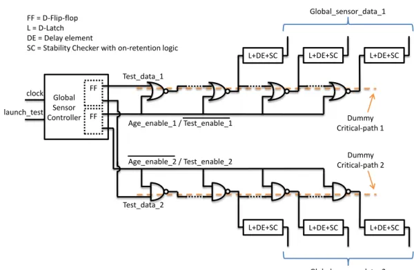
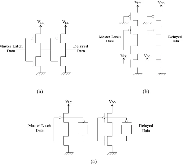
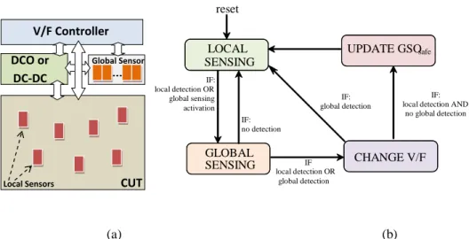
IGURESFigure 3.1 - PMOS NBTI versus time illustrating both degradation and recovery. .... 20 Figure 3.2 - Hot carrier effects. ... 22 Figure 3.3 - TDDB effect cross section view. ... 23 Figure 3.4 - 65nm performance vs temperature and supply voltage variability. Courtesy of [19]. ... 25 Figure 3.5 - Junction temperature across the chip’s die. ... 26 Figure 4.1 - Global Aging-Aware Performance Sensor (GAAPS) architecture... 37 Figure 4.2 - NOR gate internal structure and port-map ... 38 Figure 4.3 - NAND gate internal structure and port-map. ... 39 Figure 4.4 - L+DE+SC block internal structure. ... 40 Figure 4.5 - AEP-FF Architecture. ... 41 Figure 4.6 - Delay element typical architectures: (a) Low delay; (b) Medium delay; (c) High delay. ... 42 Figure 4.7 - Stability checker architecture with on-retention logic. ... 43 Figure 4.8 - (a) Block diagram; (b) Simplified functionality for on-line operation of the Dynamic Voltage or Frequency Tuning controller. ... 47 Figure 4.9 - VHDL simulation of the V/F Controller ... 48 Figure 4.10 - Inverter: (a) basic type; (b) current starved with output-switching; (c) current starved with power switching; (d) current starved with symmetrical load. .... 50 Figure 4.11 - Relative frequency deviation in term of temperature variation [24]. ... 51 Figure 4.12 - Relative frequency deviation in term of power supply voltage variation [24]. ... 51 Figure 4.13 - Combined ring VCOs: (a) 3 stages; (b) 5 stages; (c) 7 stages [24]... 52 Figure 4.14 - Relative frequency deviation in term of power supply voltage variation for proposed ring VCOs [24]. ... 53 Figure 4.15 - Relative frequency deviation in term of power supply voltage variation for proposed ring VCOs [24]. ... 54 Figure 4.16 - DCO architecture. ... 55 Figure 4.17 - DCO frequencies for the 8 ABC combinations. ... 56
xxiv ÍNDICE DE FIGURAS
xxiv
Figure 5.1 - Error-prediction and sensor operation. (a) Nominal PVTA conditions, with no error predicted; (b) PVTA WCC and error prediction. ... 58 Figure 5.2 - DFC-FF concept block diagram. ... 59 Figure 5.3 - AEPDFC-FF Architecture. ... 60 Figure 5.4 - DFC-FF Architecture. ... 61 Figure 5.5 - Correction Error Sensor Architecture. ... 62 Figure 5.6 - Correction Error Sensor Diagram. ... 62 Figure 5.7 - Stability Checker Architecture. ... 64 Figure 5.8 – Alternative Correction Error Sensor Architecture (Fast-CES). ... 66 Figure 5.9 – Alternative Correction Error Sensor Diagram (Fast-CES)... 66 Figure 5.10 - Schematic of circuits used to measure propagation delay with type D flip-flop, with AEP-FF, with DFC-FF and with AEPDFC-FF. ... 68 Figure 5.11 - Propagation delay definition. ... 68 Figure 5.12 - DW width definition. ... 71 Figure 5.13 - Measured DW vs Theoretical DW. ... 72 Figure 6.1 - 2-stage, 4-bit pipeline multiplier. ... 76 Figure 6.2 – AEP-FF failures vs (AEP)DFC-FF delay fault correction capability. .... 79 Figure 6.3 - Online VF Controller behavior due to VDD variations ... 82 Figure 6.4 - VFcode + GSOcode + Code Read from Global Sensor + Local Errors during VFController online operation. ... 83
L
IST OFT
ABLESTable 3.1 - Ambient temperature ranges standards. ... 26 Table 5.1 - Design Corners for Power-Supply and Temperature values. ... 67 Table 5.2 - Propagation delay measured values in ps. ... 68 Table 5.3 - Detailed comparison between Effective DW and Measured DW for DFC-FF and AEPDFC-DFC-FF with regular CES. ... 72 Table 5.4 - Summarized comparison between Effective DW and Measured DW for DFC-FF and AEPDFC-FF with regular CES. ... 72 Table 5.5 - Summarized comparison between Effective DW and Measured DW for DFC-FF with Fast-CES. ... 73 Table 5.6 - Summarized comparison between Effective DW and Measured DW for AEPDFC-FF with Fast-CES ... 73 Table 6.1 – Simulation conditions. ... 76 Table 6.2 – Simulation Conditions. ... 81
A
CRONYMSAEP-FF Adaptive Error-Prediction Flip-Flop ou Flip-Flop com
Predição Adaptativa de Erro
ASIC Application Specific Integrated Circuit, ou circuito integrado
de aplicação específica
ATPG Automatic Test Pattern Generator, ou gerador automático para
padrões de teste
IC Integrated Circuito ou Circuito Integrado
CMOS Complementary Metal-Oxide Semiconductor, ou
semiconductor de metal e óxido de lógica complementar (família lógica)
CP Critical Path, ou caminho crítico (o caminho com maior
tempo de propagação)
CST Controller and Sensor Tuning
EM Electro-Migration, ou migração eléctrica
FF Flip-flop
FPGA Field Programmable Gate Array, ou matriz de portas
programáveis
H Hidrogénio (símbolo químico)
HCA Hot Carrier Aging, ou envelhecimento por portadores quentes
HCI Hot Carrier Injection, ou inserção de portadores quentes
IT Interface Traps, ou obstáculos à passagem da corrente
eléctrica, formados no interface Si-SiO2
LTD Long Term Degradation, ou degradação em períodos de
tempo longos (referente a modelo de degradação)
NBTI Negative Bias Temperature Instability, ou instabilidade na
temperatura em polarização negativa
NMOS N-type Metal-Oxide Semiconductor, ou semicondutor de metal
xxviii INTRODUCTION
xxviii
NMOSFET N-type Metal Oxide Semiconductor Field-Effect Transistors,
ou transístor semicondutor de metal e óxido de efeito de campo do tipo N
PBTI Positive Bias Temperature Instability, ou instabilidade na
temperatura em polarização positiva
PDF Path Delay Faults, ou faltas de atrasos em caminhos
PI Primary Input, ou entrada primária
PMOS P-type Metal-Oxide Semiconductor, ou semicondutor de metal
e óxido do tipo P (transístor ou família lógica)
PMOSFET P-type Metal Oxide Semiconductor Field-Effect Transistors,
ou transístor semicondutor de metal e óxido de efeito de campo do tipo P
PO Primary Output, ou saída primária
PTM Predictive Technology Model, ou modelo preditivo da
tecnologia (referente a modelos SPICE de transistores)
PVT Process, power-supply Voltage and Temperature, ou processo
(V), tensão de alimentação (V) e temperatura (T) (variações)
PVTA Process, power-supply Voltage, Temperature and Aging, ou
processo (V), tensão de alimentação (V), temperatura (T) e envelhecimento (A) (variações)
R-D Reaction – Diffusion, ou reacção – difusão (modelo)
SI Secondary Input, ou entrada secundária
Si Silício (símbolo químico)
SiO2 Dióxido de Silício
SIV Stress Induced Voids, lacunas induzidas por stresse
SM Stress Migration, ou migração devida ao stresse
SO Secondary Output, ou saída secundária
T Temperature or Temperatura
TC Thermal Cycling, ou fase termal
TV Tabela de Verdade
TDDB Time Dependent Dielectric Breakdown, ou quebra no
dieléctrico dependente do tempo
TID Total Ionizing Dose, ou dose de ionização total (efeito
INTRODUCTION xxix
V Power-supply Voltage, ou tensão de alimentação (variações)
VHDL VHSIC (Very High Speed Integrated Circuits) Hardware
Description Language
VT Power-supply Voltage and Temperature, ou tensão de
alimentação (V) e temperatura (T) (variações)
Vth Threshold Voltage, ou tensão limiar de condução dos
1. I
NTRODUCTIONLike living organisms, integrated circuits have during its lifetime a degradation process of the initial characteristics very similar to physiological aging. Thus, this degradation process is also called aging. This is a slow and cumulative process that occurs in the circuits caused by operation time and operating conditions. The origin can be several factors, such as temperature, voltage, humidity, operation frequency, and others [1][2][7]. Aging is caused by all the mechanisms that change the circuit physical and electrical parameters reducing, this way, it is useful lifetime [2].
In addition, physiological aging usually causes decreased responsiveness to stimulus, which in digital circuits can be represented by the response time of the cells, or by the propagation time of the combinational paths associated with the lowest average conductivity of the transistors [3]. To deal with propagation time errors a safety time margin is added (usually defined as time slack, which is the time left in a period, after subtracting the propagation time of the path) to guarantee that the increased delays within the period of operation of the circuits, will not lead to a synchronism error [4]. However, if the propagation time increases further, boosted by variations in the manufacturing process (Process variations), or by variations in voltage supply (power-supply voltage variations), or by variations in the operating temperature (Temperature variations), or by aging (Aging variations), or by the sum of all effects (PVTA variations), there is a synchronism error [5]. This happens when memory cells (usually flip-flops) do not capture the correct value, but a value delayed due to the increase of the propagation time of the combinatorial paths [6]. Thus, PVT variations may cause the same errors that timing variations cause by aging. And these aging variations are cumulative, reducing the lifetime of the integrated circuit (IC), because they become slower and with higher probability to fail.
Once again, is interesting the remarkable resemblance between living organisms and circuits. Gradual degradation by aging changes the electrical parameters of the transistors and as a consequence changes the electrical parameters of the circuit [7],
2 INTRODUCTION
2
until the point that the equipment as a whole will stop working due to critical failures (equivalent to death in living organisms).
As mentioned, PVTA are key variations that could cause a circuit to fail. In our days, with the demand of limited energy and power consumption for mobile applications (cell phones, laptops, other battery powered devices), it became necessary to use Low Power (LP) design techniques for successful product development. VDD reduction and clock frequency reduction are two techniques to
reduce power dissipation in CMOS. However, parametric variations on the voltage (VDD) introduces additional constraints on the fault-free operation of a circuit, and
commonly frequency reduction is also used simultaneously, to avoid delay-fault occurrence. But certain product’s specifications may not comply with an overall performance loss.
Nowadays there are several low power techniques. Among dynamic power control techniques are: clock gating, multi power supply voltage (multi-VDD), variable
frequency, and power efficient circuits [1]. Leakage power control techniques comprise power gating and multi threshold (multi-Vth) cells. Depending on the design
complexity and requirements combination of LP techniques are adopted.
1.1 PROBLEM ANALYSIS
As mentioned, CMOS circuit’s performance is affected by many parametric variations, like Process, power-supply Voltage and Temperature (PVT) [26], as well as to aging effects (PVT and Aging – PVTA), with the Bias Temperature Instability (BTI) being one of the main concerns that affects PMOS (Negative BTI, NBTI) and NMOS (positive BTI, PBTI) transistors. All these variations degrade circuit performance and increase variability in CMOS circuits, mainly in nanometer technologies. This may lead to chip failures, especially when several effects occur simultaneously or when cumulative degradations pile up. To deal with nanometer technologies increased variability in CMOS circuits, designers use conservative approaches, with wider relative circuits’ time slacks (error margins), leading to non-optimized circuits.
INTRODUCTION 3
As technology scales down, power density is increasing, as the areas shrink and the frequencies increase, but power supply voltages stop scaling down significantly below 1 volt [29]. Dynamic power is still the main concern; however from 65nm and below, leakage power may become similar [30]. Standard techniques like clock-gating are being used to reduce dynamic power in recent server-class microprocessors [29]. However, aggressive techniques to reduce power consumption are gaining their way in battery operated applications (like Dynamic Voltage and Frequency Scaling – DVFS [12]).
Various sensor topologies have been presented, to globally detect circuit’s performance degradation [27] (some of them identified as aging sensors). However, Global Sensors age differently than the circuit and consequently, either (1) low slack margins are used allowing circuit failure, because the circuit’s critical path (CP) has higher delay degradation than the sensor, or (2) large slack margins are used, and the circuit is not optimized. More recently, Local Sensors were also presented to detect performance errors ([23], [4], [5], [16]). However, Local Sensors will only detect abnormal delays if the critical paths they monitor are activated. Therefore, they work well in off-line mode, but they are not reliable for avoiding errors in on-line operation.
1.2 OBJECTIVES
The main objective of this dissertation consists in implementing a complete aging-aware power or frequency optimization methodology, that addresses previous performance sensors’ problems, and is a continuation of the work reported in [25]. In [25] both Global Sensors and Local Sensors are used to permit a constant and on-line performance monitoring, and to allow an optimized operation, targeting reduced power consumption or high performance. Performance optimization is achieved by increasing operating frequency to the maximum limit while still preventing errors from happening. Power consumption optimization is achieved by reducing power-supply voltage (VDD) to the minimum value which can still prevent errors occurrence. The use of global and local sensors allow us to take advantage of the best of each sensor type: global sensors perform an on-line effective monitoring, whereas local sensors predict errors locally in the circuit, where they really occur.
4 INTRODUCTION
4
However, in [25] the controller to allow the complete Voltage or Frequency optimization was not implemented, it was only defined its simple behavior. Moreover, a digitally-controlled VCO (Voltage Control Oscillator) or DC-DC converter, to allow implementing the tuning of the Voltage or frequency, was also not implemented, and only the concept of sensor design and global and local sensor interaction was presented. Therefore, the main purpose of this work is to develop a new Controller and Sensor Tuning (CST) block, and also a digitally controlled VCO (DCO, Digital Control Oscillator), that allows on-line Dynamic Voltage or Frequency Scaling. This CST will receive information from the global sensor and from the local sensors and will decide and act over the DCO block (in fact, it can be either a DCO or a DC Voltage-Converter) to control the frequency (or voltage, if DC Voltage Converter was considered) of operation, according with the sensors’ information.
The first task will be to design the CST behavior in VHDL, compile it and simulate it. Then the CST must be converted in a SPICE netlist, in order to simulate the full Power and Frequency Tuning (composed by the CST, the global sensor, the local sensors and the voltage or frequency source). The final circuit must behave with the maximum performance without any errors. Every time an error is predicted, the CST must act over the voltage/frequency source.
A second and additional objective of this work is to develop a new delay-fault correction circuit, based on the previous aging sensor circuit [19], to predict or correct the occurrence of delay-faults. The concept behind circuit failure prediction and correction has a great potential, and is a huge improve in nanometer technologies. The key idea is to propose changes upon existing aging sensors’ flip-flop (FF) and to allow not only the error prediction, but also its correction, if an increase variation is achieved under additional PVTA variability.
This task starts with the design of a new reliable sensor that uses aging and PVT variability on its favor. The sensor must have low power consumption, be small, easy to be introduced locally at circuit flip-flops, where the synchronizations errors occur. A correction margin, defined by design, will allow the identification of late arrivals at FF’s data input. Under certain limits, these late arrivals should be corrected, improving circuit’s reliability.
INTRODUCTION 5
SPICE simulations will be used to create sensor’s sub-circuits and, also, benchmark circuits to test it under PVTA variations, in order to prove the circuit’s capabilities.
1.3 ORIGINAL CONTRIBUTIONS
The original contributions developed in this research work, mainly in comparison with [25] work, are:
Development of the CST and circuitry, in behavior VHDL representation, in structured gate level Verilog representation (using a generic CMOS library of 65nm BTM (Berkeley Technology Models)), and in SPICE type netlists; Specification and interconnection of a complete system, based on Frequency
tuning, using a SPICE netlist description;
Complete methodology validation, through transistor level SPICE simulation of a Circuit Under Test (CUT) and methodology circuitry;
Development of a novel Error-Correction FF, based on previous Error Prediction FF.
1.4 CONTEXT OF THE RESEARCH WORK
This thesis research & development (R&D) work was conducted at the Superior Institute of Engineering (ISE), University of Algarve (UAlg), in close collaboration with INESC-ID Lisbon. The working group of the two Portuguese institutes has been working in partnerships with other foreigner R&D institutes and universities such as the University of Vigo is Spain, the INAOE institute in Mexico and PUCRS University in Brazil. In recent years research work has been developed in the area of aging sensors for both ASIC (Application Specific Integrated Circuit) and emulated
6 INTRODUCTION
6
circuits in FPGAs (Field-Programmable Gate Array), as well as Voltage and Frequency optimization for long-term operation, both for ASIC and FPGA.
In this context, 2 M.Sc. thesis were already finished, and another one is currently being developed, in ISE-Ualg. Moreover, other M.Sc. and Ph.D. thesis were finished and are currently being developed in partner institutions, namely a Ph.D. thesis initiated in 2013 at Instituto Superior Técnico (IST) (University Partner), INESC-ID (Research Partner) and SiliconGate (Industrial Partner) in Lisbon, also in the area of Performance vs. Power optimization, but with the constraint of using commercial design tools and libraries, to allow an easier applicability to the industry.
Furthermore, this thesis pretends to continue the research work initiated in [19], to use the aging sensors developed there, along with global sensors, to optimize dynamically the Power and/or the Frequency of operation in electronic systems, and therefore develop a new DVFS (Dynamic Voltage and Frequency Scaling) methodology, compatible with PVT and aging variations.
Finally, the research work developed in this thesis was recently submitted to a definitive Portuguese Patent registration (currently pending), in August 27, 2013, under the number PT 106513, and entitled to "Optimização ao Longo da Vida da
Dissipação de Potência ou da Performance em Circuitos Integrados Digitais Síncronos" [38]. The complete patent submission is presented in the Appendix.
1.5 THESIS OUTLINE
The remainder of this thesis is organized as follows.
In Chapter 2 the state-of-the-art in Low-Power Design Techniques are presented. The problem of variability in CMOS nanometer technologies is addressed in the Chapter 3. The main effects, like Process, Temperature, Power-Supply Voltage, and Aging variations, that can degrade circuits’ performance are resumed.
In Chapter 4 is presented how the Power and Frequency tuning is achieved. Also, it is resumed the architecture of the local sensor, of the global sensor, of the controller and of the DCO.
The Delay-Fault Correction Flip-Flop (DFC-FF) architecture is presented in Chapter 5. Based on the Adaptive Error-Prediction Flip-Flop (AEP-FF) architecture,
INTRODUCTION 7
the DFC-FF allows the prediction of performance errors locally, in the critical memory cells where the errors occur, and the correction of the errors. The DFC-FF characteristics are also defined with SPICE simulations.
In Chapter 6, simulation results are presented, both for the Power and Frequency tuning methodology, and for the DFC-FF, using benchmark circuits as test vehicles. The results prove that the methodology can effectively tune the frequency of operation and coordinate global and local sensors to monitor Voltage variations, and that the new sensor FF has predictive fault-detection and correction capability.
Lastly, Chapter 7 summarizes the main conclusions and provides guidelines for future work.
2. L
OW-
POWERD
ESIGNT
ECHNIQUESIn our days, with the demand of limited energy and power consumption for mobile applications (cell phones, laptops, other battery powered devices), it became necessary to use Low Power (LP) design techniques for successful product development. VDD reduction and clock frequency reduction are two techniques to
reduce power dissipation in CMOS. However, certain product’s specifications may not comply with an overall performance loss.
Nowadays there are several low power techniques. Among dynamic power control techniques [1] are clock gating, multi power supply voltage (multi-VDD), variable
frequency, and power efficient circuits. Leakage power control techniques comprise power gating and multi threshold (multi-Vth) cells. Depending on the design
complexity and requirements it could be adopted a combination of LP techniques. This section presents a brief description of few LP design techniques used to reduce power consumption in modern Systems on a Chip (SoC) designs. For the concern of this thesis, we will focus on DVS and/or DVFS techniques.
2.1 D
YNAMICV
OLTAGE ANDF
REQUENCYS
CALING(DVFS)
FUNDAMENTALS
Dynamic voltage scaling (DVS) is a widely used technique to reduce the overall energy consumption of a processor, especially under wide workload variations [8].
Dynamic multi-VDD design strategies can be broadly classified as follows [1]:
Static Voltage Scaling (SVS): Different, but static supply voltages are applied to different blocks or subsystems of the SoC.
Multi-level Voltage Scaling (MVS): The block or subsystem of the ASIC or SoC design is switched between two or more supply voltage levels. However,
10 LOW-POWER DESIGN TECHNIQUES
10
for different operating modes, a limited number of discrete voltage levels is supported.
Dynamic Voltage and Frequency Scaling (DVFS): Supply voltages, as well as clock frequency, are dynamically varied for different operation modes, in order to improve power efficiency. When high speed of operation is required, VDD is increased to attain higher speed of operation; of course, the penalty is
increased power consumption.
Adaptive Voltage Scaling (AVS): In this design strategy, the supply voltage is controlled using a control loop. This is an extension of DVFS.
The average dynamic power dissipated by a chip using static CMOS gates is
∑ ( ) , where is the clock
frequency, is the output node capacitance of each logic element, and is the average switching activity parameter of node . is the capacitance being switched per clock cycle. [1]
Due to the quadratic dependence of energy with supply voltage, significant energy savings are achievable with DVS. However, this formula is only accurate with chips implemented using 100% static CMOS. Also, some electrical components’ efficiency decrease with increasing temperature. Hence, power consumption will increase to compensate the temperature rise. Consequently an increase in or may increase system power demands even faster than the CMOS formula indicates, and vice-versa [1].
In devices powered by batteries, DVS is widely used as part of strategies to manage switching power consumption. This leads to low voltage modes in conjunction with lowered clock frequencies to minimize power consumption used in components such as CPUs (Central Processing Unit) and DSPs (Digital Signal Processor). When computational power is needed the voltage and frequency will be raised.
There are other power conservation techniques that use the same principles as DVS, and that technique is Dynamic Frequency Scaling (DFS). Both techniques can prevent overheating in the computer system, however if the voltage supplied is reduced below the limit recommended by the manufacturer, it can result in system instability.
LOW-POWER DESIGN TECHNIQUES 11
Even though DVS, DFS or DVFS may reduce significantly power consumption, it is important to tune and , otherwise the desired performance will be sacrificed.
Nevertheless, the major difficulty is to find the “correct” values for and . This occurs because is difficult (1) to know the relationship between and ; and (2) to have a circuit that matches the critical path [1].
Enhanced Intel SpeedStep® Technology [9], AMD PowerNow!™ technology [10] and Razor [8] [12] from ARM are examples of DVS/DVFS techniques. Those techniques choose the “correct” / value based on the statistic of errors obtained. The next sub-sections will consider those techniques.
2.2 RAZOR
2.2.1 RAZOR I
Accordingly with [8], Razor (so on called Razor I) key concept is to sample the input data of the flip-flop at two different points in time. The first sample is stored in a conventional positive-edge triggered, master-slave flip-flop. This main flip-flop has a “shadow latch”, which samples at the negative edge of the clock. Thus, the shadow-latch gets additional time equal to the high-phase of the clock to capture the correct state of the data. When the data at the main flip-flop differs from the shadow-latch data an error is flagged.
Because it is allowed to violate the setup and hold constraints, it is required an additional detector to flag the occurrences of metastability at the output of the main flip-flop.
Error signals of individual Razor I flip-flops are then “OR”-ed together to generate a pipeline restore signal which overwrites the correct data in the shadow-latch into the main flip-flop, thereby restoring correct state in the cycle following the errant cycle. [8]
Because the shadow latch data will be used to overwrite state in the main flip-flop, it is required to ensure that data is always correct, and for that it will be necessary to use conventional worst case techniques.
12 LOW-POWER DESIGN TECHNIQUES
12
However, deploying Razor I for high-performance, aggressively-clocked microprocessors, creates a few key design issues. The main issue is the generation and propagation of the pipeline restore signal [11][12]. This signal is evaluated at the output of a high fan-in OR-tree and is suitably buffered and routed to every flip-flop in the pipeline stage before the next rising edge of the clock. But, this can cause the error recovery path to become itself critical when the supply voltage is scaled due to timing constraints on the restore signal. Hence, Razor I is used especially in aggressively clocked designs, as limited voltage headroom is available. Other issue is the design of the metastability detector. Due to rising process variations, it becomes difficult to respond to metastable flip-flop outputs across all process, voltage and temperature corners.
Consequently, it is necessary the use of larger devices that will impact adversely in the area and power overhead of the Razor I flip-flop. Also other risk is the metastability at the restore signal which can propagate to the pipeline control logic, leading to a potential system failure.
In order to address the design and time issues of Razor I, it was developed an improved technique called Razor II. This technique will be considered in the next sub-section.
2.2.2 RAZOR II
Razor II technique [12] moves the responsibility of recovery entirely to the micro-architectural domain. In Razor II, the processor is intended to operate near the Point of First Failure (PoFF) and recovery from a timing error occurs by a conventional architectural replay mechanism.
Razor II is significantly more amenable to high performance microprocessors due to architectural replay that greatly simplifies the error recovery path, when compared with Razor I.
The Razor II approach is based in two components which are as follows [12]: 1. Razor II only performs detection in the flip-flop, leaving correction to be
LOW-POWER DESIGN TECHNIQUES 13
complexity and size of the Razor II flip-flop, even though at the cost of increased Instructions Per Cycle (IPC) penalty during recovery. Architectural replay is a conventional technique which supports speculative operation such as out-of-order execution and branch prediction. Consequently, in the event of timing errors, it is possible to overload the existing framework to support replay. Additionally, this technique excludes the need for a pipeline restore signal.
2. The design of the Razor II flip-flop replaces the master-slave flip-flop by a positive level-sensitive latch. The flip-flop will flag any transition on the input data in the positive clock-phase as a timing error. Without the master latch, the clock-pin capacitance of the flip-flop is reduced and reducing also the power and area overhead. This allows Razor II flip-flop, without additional overhead, to detect Single Event Upsets (SEU) in the logic and registers.
In the Razor II flip-flop, the elimination of the master latch and the metastability detector are major simplifications that lead to improvements in delay, power and area. The elimination of the master latch leads to slightly improved clock delay compared to a conventional flip-flop and eliminates completely the setup time constraint at the positive edge of the clock.The total power overhead due to insertion of Razor II flip-flops in the processor is around half the power used with Razor I. The area improvement is due to completely elimination of the metastability risks at the positive edge of the clock for the latch data-path, thereby eliminating the need of a metastability detector.
2.3 INDUSTRY STANDARDS
2.3.1 ENHANCED INTEL SPEEDSTEP®TECHNOLOGY
Enhanced Intel SpeedStep® Technology is mean to achieve average power savings depending on system usage and design.
This technology [9] allows the system to adjust dynamically the processor voltage and core frequency, which can result in decreased average power consumption and
14 LOW-POWER DESIGN TECHNIQUES
14
decreased average heat production. Furthermore, this feature can help companies with power concerns due to their sites approaching the limits of bounded electrical infrastructures. Enhanced Intel SpeedStep® Technology, combined with existing power saving features, can provide an excellent balance between conserving power when you do not need it and providing it when you do.
Enhanced Intel SpeedStep® Technology architecture uses design strategies that include [9]:
Separation between Voltage and Frequency changes. By stepping voltage up and down in small increments separately from frequency changes, the processor is able to reduce periods of system unavailability (which occur during frequency change). Thus, the system is able to transition between voltage and frequency states more often, providing improved power/performance balance.
Clock Partitioning and Recovery. The bus clock continues running during state transition, even when the core clock and Phase-Locked Loop are stopped, which allows logic to remain active. The core clock is also able to restart far more quickly under Enhanced Intel SpeedStep® Technology than under previous architectures.
Because the latency associated with changing the voltage/frequency pair (referred to as P-state) is reduced by Enhanced Intel SpeedStep® Technology, those transitions can be practically undertaken more often, which enables more-granular demand-based switching and the optimization of the power/performance balance based on demand [9].
2.3.2 AMDPOWERNOW!™TECHNOLOGY
AMD PowerNow!™ technology [10] is an advanced power-management feature that reduces the overall power consumed by the processor through control of voltage and frequency. This power-saving is achieved by controlling independently the voltage and the frequency. This technology is designed to provide very fine and dynamic control of voltage and frequency.
LOW-POWER DESIGN TECHNIQUES 15
AMD PowerNow!™ technology [10] have tree modes of operation: High-Performance (where the processor runs at the maximum rated voltage and speed providing the maximum performance possible);. Power-Saver (where the processor runs at the lowest voltage and frequency supported); and Automatic (where the speed and voltage are dynamically and automatically determined by actual performance demands of the application). In the Automatic mode, is the application environment needs that dictates the amount of performance required and power used. This operation mode guarantees that only the essential amount of power is dissipated to meet the performance demands of the application.
3. V
ARIABILITY INCMOS
C
IRCUITSNowadays the demand for functional circuits is increasing. Also the reduction of size in the SoC demands that the causes of performance errors to be well know.
In this section, several causes of performance errors are addressed. A detailed analysis of all the causes of performance error is out of the scope of this thesis. The idea is to give an overall view in order to the reader understand the importance of this research work. With this in mind, and in case the reader wants exhaustive information, he is invited to obtain detailed information by consulting the references.
3.1 AGING
Aging is the process where circuits lose their initial characteristics. It is in general a change in the behavior of all the transistors of an integrated circuit. This modification which is slowly progressive and different from transistor to transistor, usually translates into a decreased ability of conducting electric current (in the case of BTI corresponds to the increase in the absolute value Vth of the transistors). However, aging is not occasional random deterioration where a component is damaged (often caused by extreme variations in the manufacturing process) or deterioration caused by operating in special situations of stress, causing irreparably damage to a component (for example, a condenser disrupting or electrical connections breaking in a component) [3].
Also, the constant size reduction in CMOS technology boosts the aging of integrated circuits. Smaller transistor’s, where the driving is done by a small number of ions and electrons, turns the circuits and components more vulnerable to external influences. Variation of any existing parameter in nanotechnologies leads to greater uncertainty in the behavior of electrical circuits and to lower energy needed to modify
18 VARIABILITY IN CMOSCIRCUITS
18
this behavior. This way the circuits became more susceptible to changes in its structure and in its behavior. Aging is thus accelerated in nanotechnologies [3].
In earlier technologies, this aging also occurred, but as the effects on the circuits were smaller, they weren’t notice during the life cycle of the circuit. The life cycle of the circuit were guaranteed by generous safety margins (time slacks). At that time it was said that the circuits practically didn’t age.
However, in nanotechnology, and more specifically in the case of digital integrated circuits, aging usually causes the increase in propagation time of the logical gates and, thus, the propagation times of the paths. If the propagation time increases, a synchronous error may occur when the time slack is not able to accommodate this increase in propagation times inside the period of the clock. In this case, the flip-flops (and the synchronous memory cells) do not capture the correct value because it arrives late in relation to the clock signal (which marks the synchronism) [13]. The existence of PVT (Process, power-supply Voltage and Temperature) variations in conjunction with the cumulative degradation caused by aging (ie, overall PVTA variations) does reduce the useful lifetime of circuits. In fact, as reported in [14], considering nanotechnology applications where safety is critical, and where the circuits average time of use are relatively high, as is the case of automotive electronics where trucks have average life time of 15 to 20 years (and where nanotechnologies is the technology frequently used [15]), the cumulative degradation caused by aging is critical for proper circuit performance. It is imperative that aging is considered in the design stage, in order to predict and ensure circuits operationally during the lifetime expected without errors, especially in new nanotechnologies [16].
The most important aging causes that cause degradation in the digital IC are [3]: Bias Temperature Instability (BTI); Hot-Carrier Injection degradation (HCI); Time Dependent Dielectric Breakdown (TDDB); and Electromigration (EM).
From all these phenomena, the BTI stands out as being the one that causes more degradation in ICs affecting the transistors.
VARIABILITY IN CMOSCIRCUITS 19
3.1.1 BIAS THERMAL INSTABILITY
In technologies under 130nm, Negative Bias Temperature Instability (NBTI) in PMOS devices has become an important reliability issue [17]. NBTI consists in the increase of the absolute threshold voltage value with time in the PMOS transistors. This will cause the circuit delay to degrade over time until the delay exceeds the circuit specifications [17].
There is also a corresponding effect in the NMOS transistors, identified as Positive Bias Temperature Instability (PBTI), and is observed when a positive bias stress is applied across the gate oxide of the NMOS device [17]. Even though PBTI impact is lower than NBTI, with the use of Hf-based dielectrics in the gate-oxide for leakage reduction, PBTI is gradually becoming more important [17].
BTI is a thermally activated process that degrades CMOS transistors’ physical parameters like threshold voltage and channel holes/electrons mobility. It occurs under negative gate voltage for PMOS (e.g. VGS = -VDD) and under positive gate voltage for NMOS (e.g. VGS = VDD) and is measured as a gradual increase in the magnitude of threshold voltage (|Vth|) with time. The result of the rise in |Vth| is the reduction of the absolute drain current (IDsat), the reduction of the trans-conductance
(gm), and the increase of absolute drain off current (Ioff). The drain current reduction
outcomes in temporal degradation in the performance of a circuit causing reliability degradation over time [19].
In a digital circuit, a PMOS transistor is conducting normally when the gate is with the logic level “0”, which is equivalent to have VGS = -VDD (an NMOS transistor is
conducting normally when the gate is with the logic level “1”, which is equivalent to have VGS = VDD). In this condition, also known as the stress stage of the transistor, the
electric field employed between the gate and channel transistor has a maximum intensity. Furthermore, if a greater thermal energy (high temperature) is applied, the conditions to break the chemical bonds (Si bonds and Si-H in the interface SiO2) are boosted, increasing the instability and creating obstacles to the drive (which reduces the mobility of holes for the PMOS or electrons for the NMOS, causing a reduction of the absolute drain current, ID). In the condition where the logic level of the gate is
high for the PMOS (VGS = 0V and VG = VDD) or low for an NMOS (VGS = 0V and
20 VARIABILITY IN CMOSCIRCUITS
20
phase. However, not all connections are re-established, which leads to a slow and cumulative degradation of the transistor (Figure 3.1). That is, considering the transistor as a switch (as in digital circuits), the time between the cutting and driving, and vice versa, will be higher [3].
Therefore, the BTI aging mechanism is causing most damage in digital IC and is currently the greatest concern to the scientific community in the field of nanotechnology and therefore the most investigated. The increase in the transistors |Vth| causes reduction of the useful life of the CMOS. This happens due to the increase of digital logic gates delay times and paths response times which leads circuits to begin to fail and, consequently, all the equipment in which they are inserted [3].
It is important to note that the NBTI effect affects the PMOS devices, and hence the rising delay of a gate, while the PBTI effect affects the NMOS transistors, and therefore the falling delay only [17]
There are several approaches to guard-banding a circuit and guaranteeing optimal performance over its lifetime, such as sizing, and synthesis, which can be categorized as “one-time” solutions that enhance appropriate guard-bands at design time [17]. This type of approaches results in huge positive slack times during the first years of operation of the circuit, and so a greater than needed power and area overhead, in comparison with a circuit designed to meet the precise specifications, at every time point, during its operation lifetime [17]. Also, adaptive control systems can be
VARIABILITY IN CMOSCIRCUITS 21
implemented using a critical path based approach. Those techniques may be used to counter the impact of aging, as well as process and temperature variations[17].
3.1.2 OTHER AGING EFECTS
Although the BTI is the dominant effect on the aging process of the CMOS transistors and integrated circuits, other factors also influence the performance degradation of the ICs. The most important are discussed in the following.
3.1.2.1 HOT CARRIER INJECTION
Besides BTI, Hot Carrier Injection (HCI) is one of the aging effects that most degrades IC’s normal operation. Similarly to BTI effect, HCI affects the transistor transitions speed between the conduction and cut states. HCI might be a limitation on transistors size reduction, since this effect is strongly dependent on design, material quality and processing parameters of the MOSFET [3]. Despite the degradation impact of HCI is less critical in comparison with NBTI, the transistors size reduction (considering the length of FETs gate), turns HCI into a mechanisms that must be considered.
The HCl phenomenon is the degradation of the threshold voltage (Vth) and mobility of the FETs under dynamic stress mode. The electrons presents in the channel that moves from source to drain are subjected to an electric field with variable intensity depending on the bias conditions, resulting in some of the same electrons being injected into the gate oxide of the transistor [3][19]. Thus, the dielectric property of the oxide ends up being affected, and this causes a reduction in the NMOS and an increase in the PMOS current capacity [18]. Consequently, the operating speed of the circuit is reduced, what could potentially cause failure during long term operation.
22 VARIABILITY IN CMOSCIRCUITS
22
This type of degradation becomes more important due to transistors’ size reduction, especially on the length of the FETs channel. As the channel length of the FET is reduced, higher switching speed is obtain, but this leads to an increase in the electric field present in the channel. This increase in the electrical field causes physical changes on the FETs gate oxide due to deposited charges therein resulting in device performance degradation [3].
HCI have a higher impact on NMOS transistors, and this form of degradation is more pronounced near the drain region and is enhanced at saturation [19][5].
3.1.2.2 TIME DEPENDENT DIELECTRIC BREAKDOWN
The Time Dependent Dielectric Breakdown (TDDB) degradation is a failure in the transistor gate oxide. This failure happens when a conductive path forms between the gate and the substrate through the oxide, and turn out to be impossible the control of the current flow between drain and source [1][19].
TDDB can be classified as hard breakdown (HBD) or soft breakdown (SBD). HBD is a catastrophic failure of the device and of the entire circuit, while SBD does destroy the transistor functionality over time. In the SBD the dielectric properties are maintained, but there is an increase of the gate current. SDB is responsible by parametric variations such as energy, delay and noise margin over time [1][19].