Tiago Gomes
da Silveira
All-optical processing systems based
on semiconductor optical amplifiers
Tiago Gomes
da Silveira
All-optical processing systems based
on semiconductor optical amplifiers
Dissertação apresentada à Universidade de Aveiro para cumprimento dos requisitos necessários à obtenção do grau de Doutor em Engenharia Electrotécnica, realizada sob a orientação científica do Doutor António Luís Jesus Teixeira, Professor Associado do Departamento de Electrónica, Telecomunicações e Informática da Universidade de Aveiro e do Doutor Paulo Miguel Nepomuceno Pereira Monteiro, Professor Associado do Departamento de Electrónica, Telecomunicações e Informática da Universidade de Aveiro.
Apoio financeiro do POCTI no âmbito do III Quadro Comunitário de Apoio.
Apoio financeiro da FCT e do FSE no âmbito do III Quadro Comunitário de Apoio.
Para os meus pais, Orlando e Helena.
o júri
presidente Prof. Doutor Luís Castro
professor catedrático na Universidade de Aveiro
Prof. Doutor Henrique José Almeida da Silva
professor associado na Universidade de Coimbra
Prof. Doutora Maria Carmo Raposo de Medeiros
Professora associada na Universidade do Algarve
Doutor Giorgio Maria Tosi-Beleffi
Investigador no Ministério Italiano de Desenvolvimento Económico
Prof. Doutor Paulo Miguel Nepomuceno Monteiro
professor associado na Universidade de Aveiro
Prof. Doutor António Luís Jesus Teixeira
agradecimentos Agradeço ao meu orientador, Doutor António Teixeira pelo permanente entusiasmo, por me fazer acreditar que “o Tiago resolve” e por me abrir as portas do mundo; ao meu co-orientador, Doutor Paulo Monteiro por me ter trazido para as telecomunicações e por acreditar em mim, mesmo quando ainda era um “imberbe” aluno de licenciatura.
Ao Daniel Fonseca agradeço o doloroso pragmatismo, a imensa paciência na revisão de artigos e as frutíferas discussões sobre tantas ideias. Ao Ruben Luís estou grato por ter sido um elemento chave no meu crescimento como cientista e como engenheiro. Ao Rui Morais e ao Rui Meleiro agradeço o companheirismo e a colaboração no laboratório. Agradeço à Ni Yan pela frutífera colaboração e por mostrar que até na ciência há um lado colorido. Ao Doutor Giorgio Tosi-Beleffi e ao Davide Forin agradeço pelo empréstimo de material experimental e pelas discussões, essenciais à realização de alguns dos testes experimentais. Ao Doutor Naoya Wada e à sua equipa estou grato por me terem aberto a porta do seu laboratório e por me terem feito sentir em casa a dez mil quilómetros de distância. Agradeço ao Mestre João Prata pela ajuda no laboratório, especialmente durante a realização do protótipo VSB. Agradeço ao Instituto de Telecomunicações de Aveiro e à Nokia Siemens Networks por me terem acolhido e por terem possibilitado este trabalho. Ao Álvaro Carvalho agradeço porque não me deixou desistir desta tese, por me facilitar a gestão de tempo e sobretudo me ter ajudado a descobrir a minha verdadeira vocação.
Ao meu tio e amigo, Paulo Silveira, agradeço pela inspiração, por ter levantado a fasquia e por há quinze anos atrás me ter emprestado uma caixa cheia de cassetes, que foi a semente para a banda sonora desta tese e da minha vida. À Ana agradeço o apoio e discussão nos primeiros trabalhos experimentais; a revisão da tese; a companhia em tantas vésperas de conferências, enquanto ensaiava as apresentações; a motivação e o sacrifício durante os meses finais de escrita em que eu “não levantava uma palha”; por me fazer ser maior do que sou; e sobretudo por dar sentido e alegria a cada um dos meus dias. Aos meus amigos de sempre e à minha família, agradecerei pessoalmente. Porque não sei de palavras para agradecer aos meus pais o sacrifício, apoio, inspiração e amizade, lhes dedico esta tese.
palavras-chave Amplificador óptico de semicondutor (SOA), modulação cruzada de ganho, modulação cruzada de fase, processamento óptico, interferómetro de Mach Zehnder com SOA, modulação óptica de banda lateral residual, conversão de formato de impulso, regeneração, conversão de formato de modulação, multiplexagem por divisão no comprimento de onda
resumo Nesta tese investigam-se e desenvolvem-se dispositivos para processamento integralmente óptico em redes com multiplexagem densa por divisão no comprimento de onda (DWDM). O principal objectivo das redes DWDM é transportar e distribuir um espectro óptico densamente multiplexado com sinais de débito binário ultra elevado, ao longo de centenas ou milhares de quilómetros de fibra óptica. Estes sinais devem ser transportados e encaminhados no domínio óptico de forma transparente, sem conversões óptico-eléctrico-ópticas (OEO), evitando as suas limitações e custos. A tecnologia baseada em amplificadores ópticos de semicondutor (SOA) é promissora graças aos seus efeitos não-lineares ultra-rápidos e eficientes, ao potencial para integração, reduzido consumo de potência e custos.
Conversores de comprimento de onda são o elemento óptico básico para aumentar a capacidade da rede e evitar o bloqueio de comprimentos de onda. Neste trabalho, são estudados e analisados experimentalmente métodos para aumentar a largura de banda operacional de conversores de modulação cruzada de ganho (XGM), a fim de permitir a operação do SOA para além das suas limitações físicas. Conversão de um comprimento de onda, e conversão simultânea de múltiplos comprimentos de onda são testadas, usando interferómetros de Mach-Zehnder com SOA.
As redes DWDM de alto débito binário requerem formatos de modulação optimizados, com elevada tolerância aos efeitos nefastos da fibra, e reduzida ocupação espectral. Para esse efeito, é vital desenvolver conversores integramente ópticos de formatos de modulação, a fim de permitir a interligação entre as redes já instaladas, que operam com modulação de intensidade, e as redes modernas, que utilizam formatos de modulação avançados. No âmbito deste trabalho é proposto um conversor integralmente óptico de formato entre modulação óptica de banda lateral dupla e modulação óptica de banda lateral residual; este é caracterizado através de simulação e experimentalmente. Adicionalmente, é proposto um conversor para formato de portadora suprimida, através de XGM e modulação cruzada de fase.
A interligação entre as redes de transporte com débito binário ultra-elevado e as redes de acesso com débito binário reduzido requer conversão óptica de formato de impulso entre retorno-a-zero (RZ) e não-RZ. São aqui propostas e investigadas duas estruturas distintas: uma baseada em filtragem desalinhada do sinal convertido por XGM; uma segunda utiliza as dinâmicas do laser interno de um SOA com ganho limitado (GC-SOA).
Regeneração integralmente óptica é essencial para reduzir os custos das redes. Dois esquemas distintos são utilizados para regeneração: uma estrutura baseada em MZI-SOA, e um método no qual o laser interno de um GC-SOA é modulado com o sinal distorcido a regenerar.
A maioria dos esquemas referidos é testada experimentalmente a 40 Gb/s, com potencial para aplicação a débitos binários superiores, demonstrado que os SOA são uma tecnologia basilar para as redes ópticas do futuro.
keywords Semiconductor optical amplifiers (SOA), gain modulation (XGM), cross-phase modulation (XPM), all-optical processing, Mach-Zehnder interferometer with SOA (MZI-SOA), optical vestigial sideband (OVSB), pulse format conversion, modulation format conversion, regeneration, wavelength division multiplexing (WDM), optical time division multiplexing (OTDM).
abstract This thesis investigates and develops all-optical processing devices for wavelength division multiplexing networks (DWM) of the future. The ultimate goal of optical networks is to transport and deliver a densely multiplexed spectrum, populated by ultra-high bit rate signals over hundreds or thousands of kilometers of optical fiber. Such signals should be transported and routed transparently in the optical domain, without recurring to optic-electro-optic (OEO) conversions, avoiding its limitations and costs. Semiconductor optical amplifier (SOA) based technology is a promising building block due to its inherent ultra-fast and efficient non-linear effects, potential for integration, low power consumption and cost.
Wavelength converters are the basic optical functionality to increase the network throughput and avoid wavelength blocking. Methods to increase the operation bandwidth of cross-gain modulation (XGM) converters are studied and experimentally assessed to enable operation beyond the physical constraints of SOA. Single and multi-wavelength conversion exploiting cross-phase modulation (XPM) in Mach-Zehnder interferometer with semiconductor optical amplifiers (MZI-SOA) is tested.
High bit rate DWDM networks require optimized modulation formats with enhanced tolerance to fiber impairments and reduced spectral tolerance. As a consequence, it is crucial to develop all-optical modulation formats between legacy on-off-keying networks and networks employing advanced modulation formats. An all-optical format converter between optical double sideband (ODSB) and optical vestigial sideband (OVSB) based on SOA self-phase modulation is proposed and thoroughly characterized by simulations and experimental tests. A converter, which uses a mix of XGM and XPM to allow simultaneous pulse and modulation format conversion to the carrier suppressed format, is proposed.
The interface between ultra-high bit rate transport networks and lower bit rate access networks requires optical pulse format conversions between return-to-zero (RZ) and non-return-to-return-to-zero (NRZ). Two different structures are proposed and investigated. The first is based on detuned filtering of XPM converted signal; while the second uses the dynamics of the internal laser of a gain-clamped SOA.
All-optical regeneration is one of the most sought functionalities to reduce network costs. Regeneration is achieved in this work through two simple setups: a MZI-SOA based structure, and a method in which the internal laser from a GC-SOA is modulated with the input distorted signal.
Most applications are experimentally validated at 40 Gb/s, with potential for even higher bit rates, demonstrating that SOA can be one of the key elements for the next generation of optical networks.
1
Index ... 1
List of acronyms and abbreviations ... 5
List of symbols ... 11
Chapter 1
Introduction ... 15
1.1
Context ... 15
1.2
Motivation ... 16
1.3
Thesis objectives and outline ... 18
1.4
Main contributions ... 20
Chapter 2
Semiconductor optical amplifiers... 23
2.1
Motivation ... 23
2.2
Historical development... 23
2.3
Principle of SOA operation ... 24
2.4
Design of SOA ... 25
2.4.1 Materials and structures for the active layer... 27
2.4.2 Semiconductor optical amplifiers with specific design ... 28
Reflective semiconductor optical amplifier (R-SOA)... 28
Multi-electrode semiconductor optical amplifier (ME-SOA) ... 29
2.5
Gain and phase dynamics in SOA ... 29
2.6
Modelling of signal amplification in SOA ... 32
2.6.1 Gain dynamics ... 34
2.6.1.1 Inter-band processes ... 35
2.6.1.2 Intra-band processes ... 36
2.6.2 Phase dynamics ... 37
2.7
SOA simulation tool ... 38
2.8
Gain-clamped semiconductor optical amplifiers... 40
2.9
Applications of SOA ... 42
Linear Amplifier... 43
Optical modulator and detector ... 44
Wavelength Conversion ... 44
Logic gates ... 45
Multiplexing and add-drop multiplexing ... 46
Clock Recovery and Regeneration ... 46
Other applications ... 47
2.10 Summary ...47
Chapter 3
Wavelength Conversion ... 49
3.1
Motivation...49
3.2
Wavelength conversion techniques with SOA ...52
3.2.1 Cross gain modulation... 52
3.2.2 Cross phase modulation ... 53
3.2.2.1 Filter assisted XPM wavelength conversion ... 54
3.2.2.2 XPM converters with standard-mode interferometric structures ... 56
Mach-Zehnder interferometer with SOA (MZI-SOA)... 56
Michelson interferometer with SOA (MI-SOA) ... 57
3.2.2.3 XPM converters with differential-mode interferometric structures ... 58
Differential mode MZI-SOA... 59
Semiconductor Laser in a Loop Mirror... 60
Delayed-Interference Signal Converter... 61
Comparison with fiber based interferometer structures ... 62
3.2.2.4 Gain Transparent Operation ... 63
3.2.3 Four-wave mixing ... 63
3.2.4 Cross-Polarization Rotation ... 65
3.3
Enhancement of cross gain modulation bandwidth ...66
3.3.1 Decrease of the SOA effective carrier lifetime ... 66
3.3.2 XGM bandwidth enhancement by detuned filtering ... 69
3.3.2.1 Operation principle... 69
3.3.2.2 Simulation tests and filter optimization ... 71
10 Gb/s results... 71 40 Gb/s results... 77 3.3.2.3 Experimental validation ... 78 10 Gb/s results... 79 20 Gb/s results... 80 40Gb/s results... 81
3.4
Filter assisted wavelength conversion in GC-SOA ...82
3.5
Experimental characterization of MZI-SOA based wavelength converter ...88
Static characterization ... 89
Standard mode characterization ... 91
Differential mode characterization... 93
Comparison between standard and differential modes ... 94
3.6
Multi wavelength conversion ...95
3.6.1 Experimental results ... 96
3.7
Summary ...102
Chapter 4
Modulation format conversion ... 105
4.1
Motivation...105
4.2
Format modulation conversion from oDSB to oVSB ...108
4.2.1 Introduction to optical sideband suppressed signals ... 108
Electro-optical SSB / VSB generation ... 109
All-optical SSB / VSB generation... 110
4.2.1.2 Transmission of oSSB signals over dispersive fiber ... 110
4.2.1.3 Electrical dispersion compensation ... 111
4.2.2 All-optical generation of VSB signals with SOA... 113
4.2.2.1 Impact of non-ideal phase modulation in sideband suppression ... 115
4.2.2.2 SOA based converter operation principle... 117
4.2.3 Converter operation assessment ... 119
4.2.3.1 Results at 10 Gb/s ... 120
Tolerance to power variations of data signal and CW probe signal... 121
Input signal extinction ratio... 123
Input signal wavelength... 124
Transmission tests ... 124
Electrical dispersion compensation after direct detection ... 126
4.2.3.2 Results at 40 Gb/s ... 130
Performance with slow SOA device... 130
Back-to-back performance and sideband suppression with fast SOA device .... 132
Transmission results ... 133
4.3
On-off keying to CSRZ converter ... 136
4.3.1 Operation Principle... 136
4.3.2 40 Gb/s simulation tests... 140
4.3.2.1 CSRZ generation with SOA ... 140
4.3.2.2 Comparison with common transmitter ... 143
4.3.2.3 NRZ to CSRZ converter robustness to input signal variations ... 146
4.3.3 40 Gb/s single- and multi-channel experimental validation... 149
4.4
Summary... 153
Chapter 5
Pulse format conversions between RZ and NRZ ... 155
5.1
Motivation ... 155
5.2
RZ to NRZ converter with SOA and detuned filtering ... 157
5.2.1 Pulse format conversion based only on detuned filtering... 157
5.2.1.1 Operation principle ... 157
5.2.1.2 Simulation results ... 159
5.2.2 Pulse format and wavelength conversion based on SOA and detuned filtering 165 5.2.2.1 Operation principle ... 166
5.2.2.2 Simulation tests and optimization ... 167
40 Gb/s conversion with fast SOA device... 167
40 Gb/s conversion with slow SOA device... 175
5.2.2.3 Experimental validation... 177
40 Gb/s conversion with fast SOA device... 177
10 Gb/s conversion with slow SOA device... 184
5.3
RZ to NRZ pulse converter with GC-SOA ... 185
5.3.1 Operation principle ... 185
5.3.2 10 Gb/s experimental results ... 187
Chapter 6
Optical regeneration ... 195
6.1
Motivation...195
6.2
All-optical regeneration techniques in SOA...197
6.2.1 Non-linear gate ... 197
6.2.2 Clock recovery ... 201
6.3
2R Regeneration of OCDMA with MZI-SOA ...202
6.3.1 Experimental Setup and Operation Principle ... 205
6.3.2 Experimental OCDMA Regeneration Results ... 206
6.4
2R Regenerator using a GC-SOA...209
6.4.1 Operation principle... 209
6.4.2 Experimental regeneration of a distorted signal... 211
6.5
Summary ...215
Chapter 7
Conclusions... 217
7.1
Summary and conclusions ...217
7.2
Directions for future work ...221
References ... 223
Appendix I Publications by the author... 241
List of work published in the scope of this thesis...241
Patents... 241
Journals ... 241
International peer-reviewed conferences ... 242
Local conferences ... 244
Other publications ...244
Journals ... 244
International peer-reviewed conferences ... 245
Local conferences ... 246
Appendix II SOA devices used in this work... 249
Appendix III Performance assessment in simulations ... 253
Appendix IV Optimization and development of a prototype to convert optical
DSB to VSB ... 255
10 Gb/s prototype...256
Equipment characterization and optimization ... 257
Laser characterization ... 257
Photo-detector characterization... 258
CW power optimization ... 259
Final prototype and results... 260
Back-to-back results... 260
VSB signal generation after transmission over fiber ... 263
5
Notation Description
ADC analog to digital converter
AMI alternate mark inversion
AOWC All optical wavelength converters / conversion
ARC anti-reflection coating
ASE amplified spontaneous emission noise
BER bit error rate
BR bit rate
BP bit period
BW bandwidth
CATV cable television (originally community antenna television)
c.c. complex conjugate
CC carrier cooling
CD chromatic dispersion
CDP carrier density pulsation
CH carrier heating
CLK clock
CS carrier suppressed
CSRZ carrier suppressed return-to-zero modulation format
CW continuous wave
DC direct current
DEMUX demultiplexer
DFB distributed feedback
DFF dispersion flattened fiber
DH double heterostructure
DISC delayed-interference signal converter
DPSK differential binary phase shift keying modulation format
DQPSK differential quadrature phase shift keying modulation format
CP-QPSK coherent-detected polarization-multiplexed quadrature phase shift
keying modulation format
CSRZ carrier-suppressed return-to-zero modulation format
DSB double sideband
DWDM dense wavelength division multiplexing
EDC electrical dispersion compensation
EDFA erbium doped fiber amplifier
EOP eye opening penalty
ER extinction ratio
FBG fiber Bragg grating
FCA free carrier absorption
FP Fabry Perot
FPF Fabry-Perot filter
FP-SOA Fabry Perot semiconductor optical amplifier
FWHM full-width at half maximum
FWM four-wave mixing
GC-SOA gain clamped semiconductor optical amplifier
HNLF highly non-linear fiber
IL insertion loss
IM intensity modulated
ISOL isolator
MAI multiple access interference
MEOP modified eye opening penalty
ME-SOA multi electrode semiconductor optical amplifier
MI-SOA Michelson interferometer with semiconductor optical amplifier
MLLD model locked laser diode
MQW multi-quantum well
MWC multi-channel wavelength conversion
MZ Mach-Zehnder
MZI-SOA Mach-Zehnder interferometer with semiconductor optical amplifiers
MZM Mach-Zehnder Modulator
NF noise figure
NOLM non-linear optical loop mirror
NPS Non-linear polarization switching
NRZ non-return-to-zero
OCDMA optical code division multiple access
ODC optical dispersion compensation
oDSB optical double sideband modulation format
OEO optical-electro-optical
OEWC optoelectronic wavelength conversion
OF optical filter
OOK on-off-keying
OPS optical packet switching
OSA optical spectrum analyser
OSNR optical signal to noise ratio
oSSB optical single sideband modulation format
OTDM optical time division multiplexing
oVSB optical vestigial sideband modulation format
PBS polarization beam splitter
PC polarization controller
PD photo-detector
PDL polarization dependent loss
PIC peripheral interface controller
PLC planar lightwave circuit
PM phase modulation; power monitor
PMD polarization mode dispersion
PON passive optical network
PPLN periodically pooled lithium niobate
PRBS pseudo-random bit sequence
PS phase shift
Q-factor quality factor
QD-SOA quantum-dot semiconductor optical amplifier
QW quantum well
RC raised cosine
RES resolution
RF radio frequency
RoF radio over fiber
RZ return-to-zero
SCM sub-carrier multiplexed
SGM self gain modulation
SHB spectral hole burning
SHG second harmonic generation
SL Semiconductor laser
SLA semiconductor laser amplifiers
SLALOM Sagnac interferometer with an asymetrically placed semiconductor
optical amplifier
SLED Superluminescent Light Emitting Diodes
SLPM spatial light phase modulator
SOA Semiconductor optical amplifier
SPM self-phase modulation
SSB single sideband
SSFBG super-structured fiber Bragg grating
SSMF Standard single mode fiber
SSR sideband suppression ratio
SWC single-channel wavelength conversion
TDM time division multiplexing
TE transversal electric
TF transfer function; transversal filter
TM transversal magnetic
TOAD terahertz optical asymmetric demultiplexer
TPA two photon absortion
TW-SOA traveling wave semiconductor optical amplifier
VDL variable delay line
VOA variable optical attenuator
VODL variable optical delay line
WC wavelength converters / wavelength conversion
WDM wavelength division multiplexing
XAM cross-absorption modulation
XGM cross gain modulation
XPM cross phase modulation
XPR cross polarization rotation
1R regeneration: reamplification
2R regeneration: reamplification and reshaping
3R regeneration: reamplification, reshaping, and retiming
SC single conversion
DC dual conversion
QC quadruple conversion
LAN local area networks
11
Notation Abreviation
αint absorption coefficient in SOA by the internal waveguide loss
m(t) ac coupled electrical information signal
L active layer length
V active layer volume
CAuger Auger recombination coefficient
S average photon density inside the active region
Ij bias current of section j
TB Bit period
N carrier density
Ntr carrier density at transparency
τS carrier lifetime
RASE carrier recombination stimulated by spontaneous emitted photons
εCH CH nonlinear gain compression factor
τCH CH relaxation time
c.c. complex conjugate
σ conductivity of the medium
Γ confinement factor
dg/dN differential gain coefficient
D Dispersion parameter
Hfiber Dispersive fiber transfer function
τeff effective carrier lifetime
n effective mode index
E electrical field vector of the optical field
ε0 electrical permittivity of free space
q electron charge
N free carrier density in the conduction band or carrier density
f frequency
W full width at half maximum
G Gain
gCH gain associated with CH
gSHB gain associated with SHB
gTPA gain associated with TPA
gT gain coefficient
ng Group index
vg group velocity
mH Hilbert transform of the information signal
I injected current
ILin Input losses
Sin input photon density
∇2
Laplacian operator
αCH linewidth enhancement factor for CH
αSHB linewidth enhancement factor for SHB
αN linewidth enhancement factors for CDP
gN material gain (gain associated with intra-band processes)
z Modulation depth
fmod modulation frequency
∆N modulation of carrier density
γ non-linear parameter
ANR non-radiative processes coefficient
M Number of sections
A optical signal envelope
w optical signal angular frequency
λ optical signal wavelength
βi
Order i coefficient of the Taylor approximation to the propagation constant
ILout Output losses
Sout output photon density
φ phase modulation
h Plank constant
P polarization density
ˆx polarization unit vector
x, y, z position coordinates (Cartesian coordinates)
α roll-off factor
εSHB SHB nonlinear gain compression factor
Φ Signal phase
P Signal power
ADSB Slowly varying envelope associated with an optical double sideband signal
ADSB Slowly varying envelope associated with an optical single sideband signal
A Slowly varying envelope associated with the optical pulse
Pin SOA input power
c speed of light in vacuum
BSP spontaneous emission coefficient
RREC spontaneous recombination rate
RST stimulated recombination rate
χ% susceptibility
t, t’ time
Nst unsaturated carrier density
k0 vacuum wave number
F Waveguide mode distribution
RST stimulated recombination rate
RREC spontaneous recombination rate
τ delay
15
Introduction
1.1
Context
It is outstanding to analyse statistics of International Telecommunications Union which report, for example, that the percentage of world-wide mobile phone subscribers has grown from round 5% of world population in 1998 to an estimated 61 % in 2008 [1]. Similarly, broadband home internet connections have exploded: only 10 years ago typical home connection was just 52 Kb/s; while today 200 Mb/s are commonly offered below €100 per month [2]. Even more impressive is to look back to the middle of the 20th century, where information was sent only by wire or radio. The remarkable growth in bandwidth has been feeding the burst of new internet applications, such as peer-to-peer, YouTube, MySpace, messaging, FaceBook, Twitter, Google earth, on-line gaming, etc; TV services like high-definition, 3D, and pay-per-view are also a reality in most homes. All these services and applications have dramatically changed the paradigm of communication between human beings. People want to be connected to everyone, everywhere, at all time.
This revolution could only be possible because of optical fiber communications. In the 1970’s microwave communication systems were limited to only 100 (Mb/s)/km [3]. Such limitation was eliminated with the deployment of optical fibers and especially after the invention of the Erbium doped fiber amplifier (EDFA) [4]. In the last two decades, optical time division multiplexing (OTDM) and wavelength division multiplexed (WDM) networks, together with advanced modulation formats, have led to an explosion of the bit rate-distance product. Research records are now around 117 000 Tb/km [5]. Commercial
systems are keeping up: Nokia Siemens Networks plans to provide 96 x 100 Gb/s systems during 2011 and have already an eye in 400 Gb/s per channel [6].
Although deployed transmission capacity is only one step behind research, most signal processing, such as wavelength conversion, routing, and regeneration are still done in the electrical domain. Electrical signal processing may be the next impairment to the
Holy Grail of service providers, which is to increase available bandwidth at the lowest
costs possible. The price of a single regenerator for 40 Gb/s is today several times the cost of an EDFA, for example; and the high electrical consumption of electrical processing systems is becoming a major concern for operators [7]. All-optical processing is expected to overcome such limitations and to lead optical communications to the next level. However, all-optical processing is not yet a reliable solution; therefore, it is considered a key research topic.
The main objective of this thesis is to contribute to the study and development of all-optical processing devices, focusing on some of the decisive requirements of commercial systems: low cost, simplicity and robustness.
1.2
Motivation
The functionalities required from an optical network are increasing rapidly. Years ago it was sufficient that an optical system would transmit high volumes of information over large distances. Nowadays, it is also required that the optical network performs signal processing over the information being transported.
Optical networks are now a mix of dense wavelength division multiplexing, and optical time division multiplexing [8], [9]. In DWDM several signals at different wavelengths are combined in the same optical fiber with outstanding spectral efficiency. Latest reports present efficiencies in the order of 7.7 b/s/Hz by the use of optical frequency division multiplexing [10]. OTDM consists in interleaving several incoming signals in the same wavelength, reaching ultra-high per-channel bit rates. Currently, all this information is processed in the electrical domain to achieve the required functionalities, which consist mostly in:
• Wavelength conversion: where an input signal at wavelength λ1 is converted to λ2. Wavelength converters are key devices to increase network throughput and avoid wavelength blocking.
• Regeneration: optical signals are distorted by several impairments in fiber transmission (such as dispersion, non-linearities, polarization mode dispersion (PMD), noise from amplification) and in the switching nodes (tight filtering, crosstalk, etc.). Regeneration consists in converting a distorted signal in an undistorted one.
• Format conversion: different network scenarios require different optical modulation or pulse format. Therefore, the nodes at the edge of such networks are required to convert the optical signals to the appropriate format.
Performing such operations in the electrical domain generally leads to a bottleneck-effect, since the optical transmission capacity and costs keep improving but the processing
capabilities are limited by slower, more expensive and in general less efficient electronics. It becomes urgent to develop all-optical functionalities which will enable the ultimate goal of building true fully optical routers. Besides the aforementioned essential functionalities, the following are also mandatory:
• Add-drop multiplexing: since OTDM carries the information of several users, it is require to add / extract channels at switching nodes.
• Switching: the optical signal is switched through the network from the transmitter to the end receiver. The information required for the switching is carried together with the optical signal (e.g. label). Such information should be extracted and added from the optical signal without optical-electro-optical (OEO) conversions.
• Optical memory: required to store the optical signal while the several processing functionalities are performed.
All-optical functionalities are usually achieved by exploiting the non-linear characteristics of optical mediums. Most research has focused on optical fiber, (mostly highly linear fibers [11]) and semiconductor optical amplifiers (SOA) [12] as linear mediums. In fiber, the interaction between the signals and the medium is called non-resonant [13] and has an ultra-fast response time (in the order of the femto-seconds); however, the efficiency is usually low, since the non-linear coefficients are relatively low. As a consequence high input optical power or large interaction lengths (hundreds of meters) are commonly required to achieve reasonable non-linearity. On the other hand, SOA have a much higher linear coefficient [13], but the temporal response of its non-linear applications is limited to tens or hundreds of picoseconds by slow carrier dynamics. Nevertheless, ultra-fast SOA operation is being enabled using, for example, a Mach-Zehnder Interferometer structure with SOA in each arm (MZI-SOA), operated in a differential mode. SOA have also the advantage of being integrable, have potential for low cost, provide optical gain, are stable, and can be operated with very simple schemes. State- of-the-art research demonstrates simple operations at ultra-high bit rates, such as wavelength conversion at 640 Gb/s [14], or add-drop multiplexing at 160 Gb/s [15]. However, it is still essential to investigate and develop more complex functionalities which will enable the true and effective all-optical processing capabilities of the networks of the future.
1.3
Thesis objectives and outline
The objective of this thesis is to contribute for the development of all-optical functionalities, which may constitute the building blocks for the all-optical routers of the future. It is not the objective of this work to propose or develop a routing solution, as research is not yet at the level where realistic all-optical routers can be developed. We focus on surpassing the SOA inherent limitations, such as slow response time or signal degradation due to intra-channel distortion, and on developing some of the urgent network requirements, such as wavelength converters, pulse and modulation format converters, and regenerators.
This thesis is organized in five chapters where several SOA based functionalities are investigated, the present introduction chapter, and a conclusion chapter.
Chapter 2 presents an overview of the fifty year history behind SOA
developments. An overview of the principle behind amplification in semiconductor materials is delivered, and techniques employed for the design of more efficient SOA. Different SOA-based solutions, like multi-electrode SOA (ME-SOA), gain-clamped SOA (GC-SOA) or reflective SOA (R-SOA) are revised and different network applications are pointed for each of them. The non-linear behavior of SOA is detailed regarding gain and phase dynamics. Such dynamics are the base of all applications studied throughout this work. The simulation model considered in the rest of this work is presented. This chapter includes also the state-of-the-art regarding several applications of SOA.
Chapter 3 is focused in wavelength conversion. This is most basic all-optical
functionality and the principles behind it are fundamental for the development of other processing functionalities. Wavelength converters are divided in four main groups, depending on the main non-linear effect involved: phase modulation (XPM), cross-gain modulation (XGM), cross-polarization rotation (XPR), and four-wave mixing (FWM). From these, cross-phase modulation and cross-gain modulation are chosen to perform most of the functionalities along this thesis, due to their superior characteristics: robustness to variations in the input signal like polarization, power and wavelength; allow simple processing schemes, which operate at ultra-high bit rates; versatile configurations can be obtained by combining these two non-linear effects. We experimentally demonstrate methods to enhance the operation bandwidth of XGM based on detuned filtering. A method to convert phase modulation to intensity modulation, based on detuned optical filtering, is applied for the first time in a gain-clamped SOA wavelength converter. Phase-to-intensity conversion in a MZI-SOA is experimentally characterized at 10 Gb/s and 40 Gb/s 1 to 4 multi-wavelength conversion in MZI-SOA is experimentally demonstrated.
In Chapter 4 two novel format converters are proposed. First, a format modulation
converter from optical double sideband (oDSB) to optical vestigial sideband (oVSB) is presented. The converter is based on self-phase modulation (SPM) non-linear effect. The converter operation is enhanced by the use of a continuous wave signal (CW) holding beam, which avoids distortion caused by self-gain modulation (SGM). Operation is
demonstrated by simulations and experiments at 10 Gb/s and at 40 Gb/s. After characterization in back-to-back, the converted signal is transported over optical fiber to assess its transmission properties. Two scenarios are considered: without any optical or electrical dispersion compensation (ODC and EDC), and with simple EDC. A second modulation format converter, from on-off keying to carrier suppressed return-to-zero, is proposed. The proposed scheme, which exploits the interaction between XGM and XPM in a SOA, is first compared via simulations with the common transmitter. Afterwards, single- and multi-channel operation up to four channels are experimentally assessed at 40 Gb/s.
Chapter 5 focuses on format conversions between return-to-zero (RZ) and
non-return-to-zero (NRZ) pulse formats. Two schemes to convert RZ to NRZ are proposed and experimentally demonstrated. The first uses a detuned optical filter and XPM in a SOA. The optical filter shape is optimized and approximated by Gaussian filters. Characterization is presented at 10 Gb/s and at 40 Gb/s. The second method employs a two stage structure: in the first stage the gain-clamped SOA internal laser is modulated with the data signal; the second stage consists in XGM in a common SOA. Demonstration is presented at 10 Gb/s for different pulse width at input.
Optical regeneration is studied in chapter 6. A MZI-SOA structure is employed for
the first time to suppress multiple access interference (MAI) noise of coherent 8 chip 10 Gb/s OCDMA signals. A novel 2R regeneration scheme is proposed, which uses the modulation of the internal laser of a gain-clamped SOA. This regenerator is experimentally tested at 2.5 Gb/s.
Chapter 7 delivers a summary of the work and the main conclusions. Proposals for
future work are also presented.
1.4
Main contributions
The most important results presented in this thesis are:
• Study of the cross-gain modulation (XGM) bandwidth limitation imposed by the effective carrier lifetime.
• Exploitation of a scheme which employs detuned optical filtering to convert phase to intensity and enhance up to 40 Gb/s the modulation bandwidth of a SOA device originally designed for operation at 2.5 Gb/s.
• Investigation of a wavelength converter based on cross-phase modulation (XPM) in a Mach-Zehnder interferometer with SOA (MZI-SOA). Operation is enabled over single and multi-input signals at 40 Gb/s. This work resulted from collaboration with the Technical University of Eindhoven, Netherlands.
• XPM wavelength conversion in a gain-clamped SOA is proposed and assessed at 10 Gb/s.
• A novel all-optical converter between optical double sideband (ODSB) and optical vestigial sideband (OVSB) is proposed and demonstrated at 10 Gb/s and 40 Gb/s. To the authors knowledge this is the first true all-optical converter between these modulation formats that does not require optical filtering. The converter is characterized regarding robustness to optical fiber transmission and application in real networks.
• Characterization of return-to-zero (RZ) to non-return-to-zero (NRZ) pulse format converter based on detuned filtering of a XPM signal with demonstration at 10 Gb/s and 40 Gb/s.
• Proposal of a scheme to convert RZ to NRZ based on modulation of the internal laser of a gain-clamped SOA and assessment of its performance at 10 Gb/s with ultra-short input optical pulses. This work was developed in a joint collaboration with ISCOM, Rome, Italy.
• Proposal and implementation of converter from NRZ to RZ with simultaneous format conversion to carrier-suppressed. Experimental demonstration over 40 Gb/s single and multi-input.
• Regeneration of multi-access interference (MAI) of an optical coded division multi access (OCDMA) signal with MZI-SOA. This work was developed in a joint collaboration with NICT, Tokyo, Japan.
• Proposal of the use of gain-clamped SOA to obtain true 2R regeneration and demonstration at 2.5 Gb/s.
From this work resulted a total of three patent applications, eight journal papers, nineteen international conference papers, and five national conference papers. Appendix I lists the contributions resultant from this work.
Effective research can not be done without sharing of knowledge, ideas, and facilities. This work includes the result of four collaborations: with University College of London (UCL), to characterize the dynamic response of SOA; with ISCOM, Rome, to explore the immense potentials of gain-clamped SOA; with the Technical University of Eindhoven (TuE) to experimentally develop efficient multi-wavelength applications; and with NICT, Japan to demonstrate the application of SOA-based devices in OCDMA networks.
The work developed has been framed in a PhD program in an industrial environment at Nokia Siemens Networks (NSN) Portugal, S. A. (formerly Siemens, S. A.). NSN is one of the main optical network vendors in the market and leads research and development (R&D) of optical network solutions. As a consequence, this work has been earthbound by the premises and requirements of a demanding industry: low costs, simplicity, robustness, and potential for fast integration in real products. Some evidences of this link are the three patent applications filed during the development of this work, the development of a prototype for a modulation format converter, used internally in NSN in comparison with other solutions (detailed in appendix IV), and a very strong focus on the cost, simplicity and robustness of solutions.
23
Semiconductor optical amplifiers
2.1
Motivation
Semiconductor optical amplifiers (SOA) are the key device for the all-optical processing functionalities studied and proposed in this thesis. This chapter presents an overview of the history behind the development of SOA and of some basic design principles to optimize its characteristics. Propagation of optical signals in SOA is analysed via gain and phase dynamics. The simulation model utilized throughout this work is detailed, which includes intra- and inter-band effects. Finally, the most relevant linear and non-linear applications of SOA are presented.
2.2
Historical development
The development of semiconductor optical amplifiers (SOA) is closely related to progresses in semiconductor lasers (SL) technology. The first SOA were regular laser diodes biased below threshold [12]: SOA are also know as semiconductor laser amplifiers (SLA) in the early literature [16], [17], [18]. In 1966, anti-reflection coatings (ARC) were proposed to reduce the optical feedback and allow amplification of infrared light [19]. The double heterostructure was demonstrated in 1969 and led to significant improvements in both lasers and SOA, such as enabling operation at room temperature [20]. Whilst first studies focused AlGaAs SOA, operating in the 830 nm range [21], in the 80’s decade InP/InGaAsP SOA were designed for operation in the 1300 nm and 1550 nm ranges [16].
By the second half of the 80’s the first transmission tests employing SOA as in-line amplifiers were reported [22]; however, in 1987 the Erbium doped fiber amplifier (EDFA) was invented [4] and began to compete with SOA for linear amplification purposes. The first true travelling wave SOA (TW-SOA) are reported in the end of the 80’s [17]. These devices are enabled by developments in anti-reflection coatings and feature low polarization sensitivity – one of the main drawbacks of early SOA. By mid 90’s the first semiconductor amplifiers featuring simultaneously high gain, high saturation power, and low polarization dependence are reported [23]. More recently, quantum-dot SOA (QD-SOA) have been developed to provide higher cross signal independence, lower biasing currents and wider operation bandwidths, along with other advantages [24].
Currently, SOA are presented as enabling devices for low cost amplification and processing in access networks [25], [26], since these can be used in photonic integrated circuits [27], allowing integration with several other optical components – passive or active. Moreover, SOA are compact, electrically pumped, have a large optical bandwidth, and allow flexibility in the choice of the peak gain wavelength. Due to their non-linear characteristics and fast response, SOA are also key devices for state-of-the-art all-optical processing at ultra-high bit rates (BR) [28].
The increase in the per channel bit rate and in the total number of wavelength multiplexed channels are exhausting the electrical processing capabilities of networks. Electrical processing at ultra high bit rates, such as 40 Gb/s and superior has high costs, footprint and energy consumption [29]. As a consequence, all-optical processing is currently one of the key research topics in optical networks [30].
2.3
Principle of SOA operation
The operation of semiconductor optical amplifiers requires bringing together a p-type semiconductor and an n-type semiconductor to form a p-n junction. The denominations n- and p-type refer to the semiconductor doping with impurities that have an excess valence electron or one less valence electron, respectively, when compared to the
semiconductor atoms [31]. Figure 2-1 depicts the energy band of a p-n junction. In thermal equilibrium, the Fermi level1 must be continuous across the junction (also know as depletion region). Under such condition, the charged particles set an electrical field that prevents diffusion of electron and holes across the depletion region (Figure 2-1 a)). By applying an external electrical voltage, the built-in electrical field is reduced, resulting in diffusion of electrons and holes across the depletion region. When an electron and a hole are present in the same region, recombination can occur, and a photon is produced. A photon may be generated through stimulated or spontaneous emission. Spontaneous emission originates photons with random phase and frequency; these are essentially noise
and contribute to reduce the optical gain. On the other hand, stimulated emission is the
mechanism responsible for the optical gain: the newly generated photon is identical to an emitting photon. Besides the radiative mechanisms, referred before, in a semiconductor material electrons and holes can also recombine non-radiativelly. These recombinations are not beneficial to the amplifier operation, thus efforts are made to its minimization.
Depletion Region n-type p-type Fermi level e n er g y distance n-type p-type Fermi level e n er g y distance Fermi level Emitted Photon Depletion Region
a) Thermal equilibrium; b) Under forward bias.
Figure 2-1: Energy band diagram of a homostructure p-n junction [31].
2.4
Design of SOA
Since the development of the first SOA devices, efforts have been made to improve their characteristics [12] for application in optical networks. Ideally, an optical amplifier should feature the following characteristics:
• High gain, bandwidth, and saturation power; • Negligible reflections at the end facets; • Efficient coupling at the input and output; • Polarization independent amplification; • Low spontaneous emission noise;
• Low bias current sensitivity; and low temperature dependence.
To meet such requirements, it is required to optimize the SOA design. The SOA structure is usually a double heterostructure [31], where the active layer is sandwiched between layers with different band gap energies. This configuration enables better confinement of the carriers to the active region, improving the device efficiency. Undesired reflections can be minimized through the simultaneous use of several methods, which have enabled reflectivities lower than 10-5 [32]:
• Use of antireflection coating (ARC) at the end facets of the device [33]; • Utilizing angled facet structure, where the active region is not perpendicular
to the facet cleavage plane [34];
• Guard a transparent region between the active layer and the active region end facets: window-facet structure [35].
antireflection coating transparent region taper region Active region (InGaAsP) metallisation H+-InP n-InP H+-InP p-InP
metallisation Active region (InGaAsP)
a) Cross section; b) Top view with angled facet structure.
Figure 2-2. Schematic representation of a buried ridge stripe SOA [13].
Polarization independence is usually achieved by the use of a waveguide with a square cross section (and taper region to improve coupling efficiency). Other techniques can also be employed to enable polarization independence: ridge-waveguide SOA, and
structures based on strained materials. In Figure 2-2 a schematic representation of a buried ridge stripe SOA is depicted, showing some of the design techniques referred before [13].
Semiconductor optical amplifiers are often classified in two main types depending on the facet reflectivity [18]: Fabry Perot (FP) amplifiers and travelling wave amplifiers (TW). A FP-SOA is a resonant amplifier while TW-SOA features reduced facet reflectivity. Due to their characteristics, TW-SOA have replaced FP-SOA in most applications. Consequently, TW-SOA will be simply referred as SOA hereafter.
2.4.1
Materials and structures for the active layer
The type of material and the structure of the active region determine the behaviour of the SOA regarding unsaturated gain, gain spectral bandwidth, central wavelength, polarization dependence, etc. The most common structures are: bulk, and quantum well [31]. In a bulk material all the dimensions of the active layer are significantly larger than the deBroglie wavelength, and the energy levels of the electrons and holes in the active region are continuum [31]. In quantum well (QW) materials, the active region has one or
more dimensions (usually thickness) of the order of magnitude of the deBroglie wavelength. Single QW devices have low carrier and optical confinement and high polarization dependence; therefore, are not commonly employed. Such drawbacks are avoided by the use of multi-QW (MQW). MQW materials have a series of stacked thin active layers separated by thin barrier layers [32]. MQW devices have discrete energy density levels; therefore, the dependence with the photon energy (thus, its frequency) decreases: larger gain bandwidth is achieved [32]. MQW also present improved noise figure, higher optical gain, and higher saturation power [12]. On the other hand, bulk devices may be more interesting to non-linear applications, since these usually feature large optical confinement and phase to amplitude coupling.
SOA employing quantum dot materials (QD-SOA) are currently blooming and being intensively studied. The active layer consists on nano-size semiconductor islands spatially isolated, which exchange carriers with a wetting layer; therefore, the energy states in the active layer are discrete. QD-SOA are still under research, but it is expected that when mature they will present the following characteristics [36], [37]:
• Ultrafast gain recovery (order of the picoseconds); • Low noise figure;
• Broadband gain;
• High saturation output power; • High four wave mixing efficiency; • Low threshold current;
• Low patterning effects; • Multi wavelength conversion; • Possibility of efficient 3R.
2.4.2
Semiconductor optical amplifiers with specific design
In addition to the regular SOA structure, specific design can be considered to overcome some of the SOA inherent limitations and allow particular applications.
Reflective semiconductor optical amplifier (R-SOA)
In a reflective SOA (R-SOA), represented in Figure 2-3, one of the facets is not coated with antireflective material. As a consequence, the optical beam is reflected in one of the ends, travelling twice through the active region.
Active region Antireflection coating Input beam Reflected beam
a) simplified cross section b) propagation of light inside the active region
Figure 2-3. Schematic representation of a reflective SOA (R-SOA).
Due to its reflective properties, R-SOA have been proposed to integrate a wavelength division multiplexed / sub-carrier multiplexed - passive optical network (WDM/SCM-PON) that shares the same wavelength for the up and down links [38]. The
R-SOA operates simultaneously as amplifier and optical modulator, reducing the overall cost of the network [39], [40]. R-SOA and high-birefringence fiber Bragg grating (FBG) were used to generate broadband orthogonal pumps and tuneable broadband wavelength conversion [41].
Multi-electrode semiconductor optical amplifier (ME-SOA)
In a multi-electrode SOA (ME-SOA), schematically represented in Figure 2-4, the current bias is injected through more than one electrode. Different currents can be injected at each electrode. ME-SOA have been proposed to perform simultaneous amplification and detection [42]. ME-SOA are particularly interesting for this application since it allows the conservation of the signal DC component, and independence to temperature and bias current. ME-SOA also enable amplification, modulation, and detection in only one device [43], with reduced electrical processing. A two section SOA was used as phase modulator with intensity modulation (IM) suppression [44]. The electrical modulation signal is fed in anti-phase to the two electrodes. This combination of bias currents results in the cancellation of the overall IM, while enabling phase modulation due to the different linewidth enhancement factors of the two sections. We have proposed a similar principle to obtain independent intensity and phase modulation in a ME-SOA in [45].
Active region
I1 I2 I3 I4
Current Bias
Figure 2-4. Schematic representation of a multi-electrode SOA (ME-SOA).
I1 – I4 represent bias currents.
2.5
Gain and phase dynamics in SOA
Ideally an ideal amplifier should feature constant gain, regardless of the input power. However, the gain of amplifiers saturates for high power input signals, resulting in
different gain for input signals with different power values. This effect is usually called gain saturation and is represented in Figure 2-5. For low input / output powers, the amplifier delivers a high gain, usually know as small signal gain; as the power increases
the gain is reduced. The output power at which the gain is 3 dB bellow the small signal gain, is known as saturation output power.
g ai n [ d B ]
output optical power [dBm]
30 25 20 15 10 -- - - --15 -10 -5 0 5 10 15
-small signal gain
saturation output power
3dB
Figure 2-5. Representation of gain saturation in an optical amplifier.
In an EDFA, the gain dynamics are in the order of the milliseconds [4], whilst optical signals usually have bit periods in the order of the picoseconds. As a consequence, gain saturation occurs due to the average power of the signal being amplified, resulting in negligible inter- and intra-channel distortion. In SOA, the gain dynamics are reasonably fast: in the order of the tens of picoseconds, which is a value comparable to the pulse duration in current systems. The SOA gain saturation provokes intra and inter-channel patterning effects and newly generated frequencies, i.e. four-wave mixing (FWM). Moreover, phase modulation also occurs in the SOA due to variations of the refractive index with the input power. From the later considerations, it is evident that if a SOA is to be used as a linear amplifier, the input signal power must be carefully chosen to prevent undesired distortion effects. On the other hand, the fast gain and phase dynamics can be exploited for non-linear applications.
The gain and phase dynamics of SOA are associated to the dynamics of free carriers. The free carriers density and distribution vary due to intra-band and inter-band transitions which are represented schematically in Figure 2-6.
In inter-band transitions, carriers transfer from the conduction band to the valence band and vice versa. These transitions are determined by electrical pumping, stimulated
and spontaneous emission, non-radiative recombination, and two photons absorption (TPA) [12]. In intra-band transitions, the energy distribution of the carriers varies within the same band and is determined by: spectral hole burning (SHB), free carrier absorption (FCA), carrier heating (CH), and carrier cooling (CC) [12].
Conduction Band Inter-band transition Intra-band transition Valence Band - electron + hole
Figure 2-6. Representation of intra-band and inter-band transitions in a
semiconductor.
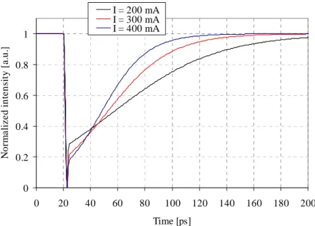
The carrier dynamics are evident through the gain response to an ultra-short optical pulse, as represented in Figure 2-7. The incoming optical pulse stimulates carriers which have energies similar to the incoming pulse photon to recombine. This provokes a hole in the carrier distribution and is associated with SHB. The carrier density within the band is also reduced via stimulated emission. Simultaneously, TPA occurs since there is a high photon density in the active region. FCA also takes place: a free carrier absorbs a photon and moves to a higher energy level in the same band. Carrier depletion is a fast process.
time o p ti ca l p ow er fast carrier deplection
fast carrier recovery via CH and SHB
slow carrier recovery via electrical pumping
time o p ti ca l g ai n
Input optical pulse
SOA optical gain
Figure 2-7. Representation of the SOA gain response to an optical pulse and
When the optical pulse leaves the SOA, the Fermi distribution is restored through carrier-carrier scattering; the related time constant is referred as SHB relaxation time. Although the Fermi distribution is restored, the carrier temperature has been increased due to stimulated emission, FCA and TPA. The temperature decreases via phonon emission; the related time constant is referred as CH or temperature relaxation time. These are fast intra-band processes. The original carrier level is then restored by means of electrical pumping, which is a slow process (hundreds of picoseconds). More information on carrier dynamics can be found in [12], [46], [47].
2.6
Modelling of signal amplification in SOA
The propagation of the electromagnetic field inside a semiconductor optical amplifier is governed by the well known wave equation [31], [48] in the frequency domain2:
( )
( )
2( )
2 2 0 0 0 0 1 i k w k w w wσ
ε
ε
∇ Ε + + ⋅Ε = − Ρ % % % , ( 2-1)where ∇2 represents the Laplacian operator,
ε
0is the electrical permittivity of free space, k0 =w c=2π λ
is the vacuum wave number, c is the speed of light in vacuum, wand λ are the optical signal angular frequency and wavelength. Ε% is the electrical field vector of the optical field, P is the polarization density arising inside the medium in response to the optical field and σ is the conductivity of the medium. Note that and Ε% and
Ρ% are complex.
Under steady state conditions the response of the medium to the electric field is governed by the susceptibility
χ
% :
2 The Fourier transform definition used throughout this work is:
( )
1( )
( )
exp 2 A w A t iwt dtπ
+∞ −∞( )
wε χ
0( ) ( )
w w Ρ% = ⋅ % ⋅Ε%( 2-2)
The full deductions of the equations that rule the pulse propagation are outside the scope of this work, more details can be found in [12], [48], [49], [50]. Hereafter only results that are required for the considered model are presented.
To enable the deduction of a simple and practical equation for pulse propagation inside the SOA, it is necessary to consider some assumptions and simplifications: the amplifier is considered to be an ideal travelling-wave amplifier whose active dimensions are such that only a single waveguide mode is allowed. Assuming that the light is linearly polarized and remains as such during the propagation, the electric field inside the amplifier can be written as [48]:
(
)
1( ) ( )
ˆ , , , , , 2 g w z i v w t x y z t x F x y A z t e ⋅ − ⋅ Ε = ⋅ ⋅ % , ( 2-3)where ˆx is the polarization unit vector, F x y
( )
, is the waveguide-mode distribution, A z t( )
, is the slow varying envelope associated with the optical pulse,/
g g
v =c n is the group velocity, ng = + ⋅n w dn dw
(
)
is the group index, and n the effective mode index.To derive the equation that governs the evolution of the pulse along the amplifier we will transform our referential in a frame moving with the pulse:
' g z t t v = − ( 2-4) ' z =z ( 2-5)
Without loss of continuity, and for simplicity of notation, the prime over t’ and z’ will be dropped hereafter. To facilitate the notation hereafter, the amplitude and phase information of the pulse are split:
( )
,( )
, exp( )
,A z t = P z t ⋅ i⋅Φ z t , ( 2-6)
With P z t
( )
, the pulse power, and Φ( )
z t, the pulse phase.2.6.1
Gain dynamics
The signal power along the SOA is described by [13]:
(
T int)
P g P z α ∂ = Γ⋅ − ⋅ ∂ , ( 2-7)Where αint is the SOA absorption coefficient caused by the internal waveguide loss,
Γ is the confinement factor, which is described by ( 2-8) and describes the gain reduction due to the spreading of the optical mode beyond the active region of the SOA.
( )
( )
2 0 0 2 , , w d F x y dx dy F x y dx dy +∞ +∞ −∞ −∞ ⋅ ⋅ Γ = ⋅ ⋅∫ ∫
∫ ∫
( 2-8)For simplicity, the confinement factor is usually assumed to be a constant. In [12] a more accurate model is presented, which includes dependence of the confinement factor with the wavelength and carrier density.
The gain coefficient g is also assumed to be independent of the wavelength and T
is given by [12] :
T N CH SHB TPA,
g =g +g +g +g ( 2-9)
With gN standing for the material gain, which reflects the contribution of inter-band
processes (carrier density pulsation); and gCH, gSHB, and gTPA stand for the gain associated
with carrier heating (CH), spectral-hole burning (SHB), and two-photon absorption (TPA), respectively.
Equation ( 2-7) can be simplified to:
( )
, in( ) ( )
,P z t =P t ⋅G z t , ( 2-10)
With Pin (t) = P(0,t) the optical power at the SOA input and G the gain, given by:
( )
(
T int)
0 , exp z G z t = Γ −gα
⋅dz ∫
( 2-11)2.6.1.1
Inter-band processes
Inter-band processes alter the carrier density, N; however, these do not affect the carrier distribution. Variations of N are also known as carrier density pulsation (CDP). The gain of the semiconductor material is directly determined by the free carrier density. The gain associated with inter-band processes is then given by [18]:
( )
(
( )
)
N , , tr . dg g t z N t z N dN = ⋅ − ( 2-12)In the previous equation, dg/dN is the differential gain coefficient, which is here assumed to be a constant; N is the free carrier density in the conduction band and, for simplicity, will referred simply as carrier density hereafter; finally, Ntr is the carrier density
at transparency (when gN=0).
The carrier density is described by [18]:
ASE ST REC
dN I
R R R
dt = eV − − − . ( 2-13)
The first right hand term in ( 2-13) represents the rate of injected electrons in the SOA active layer; with I the injected current, q the electron charge, and V the active layer volume. RASE accounts for the carrier recombination, stimulated by spontaneous emitted
photons and will be neglected here. RST is the stimulated recombination rate, described by:
ST g T