ISSN 1546-9239
© 2007 Science Publications
Corresponding Author:
Mohammad A.K.Alia, Faculty of Engineering Technology, Al - Balqa' Applied University
Using PLC for Custom-design of a PID/PWM Program to Control a Heater Temperature
Mohammad A.K.Alia
Faculty of Engineering Technology, Al - Balqa' Applied University, Jordan
Abstract:
This is a practical approach to control a continuous-time process variable (temperature)
using a discrete controller (PLC) and a custom-designed software control algorithm and hardware
interface, in a closed-loop system. Unlike the conventionally known technique of transforming a
digital control action into a proportional analogue one by a D/A converter followed by power
amplifier, the control action was formed internally by the PLC as a PID/PWM signal, which was used
to trigger the power stage. This approach helped reducing the error due D/A conversion, maximized
utilization of the PLC and reduced total cost. The control system is realized by utilizing the heater of
the training board (RGT1), manufactured by DL-lorenzo Company and it simulates an analogue
heating control system. The PLC is Siemens Simatic S7-214 model. An experimental result has shown
that the control algorithm functions perfectly.
Key words:
PLC, PID software program, PWM, PLC, analogue input digital output, interface board
INTRODUCTION
The use of a digital signal processor (DSP) to
evaluate the actual value of an analogue process output
and then compute a correction signal has many
advantages. DSP does not suffer from the long-term
drift effect that analogue circuits do. Changes to
constants can easily be made without the actual
physical change to the circuitry and simply modifying
the loaded program or loading a new one can radically
alter the mode of control. Realizing PWM techniques
and other advanced functions is some of the vast power
points of digital controllers. Actually, in most cases
DSPs are designed to replace the ON-line analogue
ones. This explains the continuous approaches to
implement digitally the traditional analogue control
modes such as PID actions.
Because of the advantages of the PLCs
[1], a PLC
type S7-200 was utilized as a DSP. Nowadays most
modern sequential control systems are based on PLCs,
which are in fact specialized industrial computers.
Thus, one of the targets of this work is to design a PLC
program for PID control algorithm and to develop it to
get at the PLC output a PWM signal proportional to the
value at the output of PID controller. In this case there
is no need for a DAC IC nor for a specific power
amplifier stage. Here the PWM signal with the power
static switch emulates the function of a D-type power
amplifier. From another side, by using the designed
interface board, one can exclude the implementation of
a high cost proprietary power interface module, this
simplifies the circuit and reduces its cost.
PLC manufacturers very often provide the option
of analogue I/O and support instant PID functions for
extra cost. Such functions can be used directly by
entering the control parameters and constants.
Nevertheless, this feature is only usable if the analogue
I/O module is installed. Therefore PID algorithm was
designed instead of using a ready one. This, also,
provides more flexibility to use the program with those
PLCs, which do not support ready PID loops. Designed
I/O board shown in Fig. 1 satisfies our demands and
costs one third of the I/O module's cost approximately.
Because of the limited size of this paper, the design
procedure of the I/O interface board is not illustrated. It
will be published in a special paper. However, I would
like to add that cost is not the only factor. As Johnson
[2]wrote: (every engineer has personal preferences as to
which flavor of PID algorithm should be used in any
particular situation). For example full PID algorithm
can only be used when the signal has little noise or
where suitable filtering or limiting has been applied.
Another example is that the derivative action could be
on the process variable only and could be on the system
error depending on the severity of change of system
error. In our study we make use of the digital values of
the PID output to initiate a PWM signal in order to
control the timing of the power switch.
R1 750Ω R7 1.2 KΩ R13 39 KΩ R19 75 Ω C1 0.1µF R2 750Ω R8 100 KΩ R14 47 KΩ P1 100 KΩ C2 100µF R3 75 Ω R9 2.2 KΩ R15 2.2 KΩ P2 500 KΩ D1 Silicon R4 15 Ω R10 1.2 KΩ R16 2.2 KΩ P3 1 MΩ D2 2.2V LED R5 120 KΩ R11 2.2 KΩ R17 1.2 KΩ P4 300 KΩ D3 Zener 5V R6 325 KΩ R12 325 KΩ R18 150 KΩ P5 2.4 KΩ -- --
Table 1: Eight parallel lines connected to eight input points of the PLC convey the instantaneous temperature value
Input number Input point
0 Æ I 1.0
1 Æ I 0.1
2 Æ I 0.2
3 Æ I 0.3
4 Æ I 0.4
5 Æ I 0.5
6 Æ I 0.6
7 Æ I 0.7
Table 2: PLC program written in ladder diagram and statement list forms and illustrated network by network Network 1
LAD STL
SM0.1 Q0.0
├─────┤├────┬────────( S )
│ 0
└────────(CALL)
LD SM0.1 S Q0.0,1
CALL 0
- On first scan, set image register bit "High". - Call SUBROUTINE 0.
- First scan is indicated by the special memory bit SM0.1 Network 2
LAD STL
│ ┌───────┐
│ SM0.0 │ ATCH │
├──────┤├───────┤EN │
│ 1 ┤INT │
│ 0 ┤EVENT │
│ └───────┘
LD SM0.0
ATCH 1,0
- SM0.0 is a special memory bit always set high (=1)
- The PWM output (Q0.0) is fed back to (I0.0) [see hardware connection] - Here, we attach the rising edge event of (I0.0) to INT1.
Network 3
LAD STL
┌───────┐
SM0.0 │ MOV_B │
├─────┤├─────────┤EN │
IB0 ┤IN OUT├ VB0
└───────┘
LD SM0.0
MOVB IB0,VB0
- Transfer the status of all inputs (I0.0,I0.1 … I0.7) as a Byte called (VB0) containing the process variable value .
- Note: this action involves (I0.0), which is not technically a process variable bit, for instance, this will not cause errors and shall be treated soon.
Network 4
LAD STL
│ I1.0 V0.0
├────────┤ ├──────( )
│
LD I1.0 = V0.0
- Correcting the last network, replace the misplaced (V0.0) coming from (I0.0) with the actual bit obtained from (I1.0) Network 5
LAD STL
┌───────┐
SM0.0 │ MOV_W │
├─────┤├─┬────────┤EN │
│ VW10 ┤IN OUT├ VW20 │ └───────┘ │ ┌───────┐ │ │ MOV_W │ ├────────┤EN │ │ SMW28 ┤IN OUT├VW10 │ └───────┘
LD SM0.0
MOVW VW10,VW20
│ ┌───────┐ │ │ SUB_I │ └────────┤EN │ VW0 ┤IN1 │ VW10 ┤IN2 OUT├ VW10
└───────┘
-I VW0,VW10
Each program cycle:
- Store previous error in (VW20).
- Store the set point value in (VW10), this value is generated using analog adjustment feature of CPU-214.
- Subtract the process variable PV (VW0) from the set point Sp (VW10) and get the result representing ERROR stored in (VW10). Network 6
LAD STL
┌───────┐
SM0.0 │ MOV_W │
├─────┤├─┬────────┤EN │
│ Kp ┤IN OUT├ VW30 │ └───────┘ │ ┌───────┐ │ │ MOV_W │ ├────────┤EN │ │ Ki ┤IN OUT├ VW40 │ └───────┘ │ ┌───────┐ │ │ MOV_W │ ├────────┤EN │ │ Kd ┤IN OUT├ VW50 │ └───────┘ │ ┌───────┐ │ │ MOV_W │ ├────────┤EN │ │ VW20 ┤IN OUT├ AC0 │ └───────┘ │ ┌───────┐ │ │ MUL │ ├────────┤EN │ │ VW30 ┤IN1 │ │ AC0 ┤IN2 OUT├ AC0 │ └───────┘ │ ┌───────┐ │ │ MOV_W │ ├────────┤EN │ │ VW20 ┤IN OUT├ AC1 │ └───────┘ │ ┌───────┐ │ │ ADD_I │ ├────────┤EN │ │ VW10 ┤IN1 │ │ AC1 ┤IN2 OUT├ AC1 │ └───────┘ │ ┌───────┐ │ │ MUL │ ├────────┤EN │ │ VW40 ┤IN1 │ │ AC1 ┤IN2 OUT├ AC1 │ └───────┘ │ ┌───────┐ │ │ MUL │ ├────────┤EN │ │ 1000/2 ┤IN1 │ │ AC1 ┤IN2 OUT├ AC1 │ └───────┘ │ ┌───────┐ │ │ADD_DI │ ├────────┤EN │ │ AC1 ┤IN1 │ │ AC0 ┤IN2 OUT├ AC0 │ └───────┘
LD SM0.0
MOVW Kp,VW30
MOVW Ki,VW40
MOVW Kd,VW50
MOVW VW20,AC0
MUL VW30,AC0
MOVW VW20,AC1
+I VW10,AC1
MUL VW40,AC1
MUL 1000/2,AC1
│ ┌───────┐ │ │ MOV_W │ ├────────┤EN │ │ VW10 ┤IN OUT├ AC1 │ └───────┘ │ ┌───────┐ │ │ SUB_I │ ├────────┤EN │ │ VW20 ┤IN1 │ │ AC1 ┤IN2 OUT├ AC1 │ └───────┘ │ ┌───────┐ │ │ MUL │ ├────────┤EN │ │ VW50 ┤IN1 │ │ AC1 ┤IN2 OUT├ AC1 │ └───────┘ │ ┌───────┐ │ │ DIV │ ├────────┤EN │ │ 1000 ┤IN1 │ │ AC1 ┤IN2 OUT├ AC1 │ └───────┘ │ ┌───────┐ │ │ADD_DI │ └────────┤EN │ AC1 ┤IN1 │ AC0 ┤IN2 OUT├ AC0
└───────┘ MOVW VW10,AC1 -I VW20,AC1 MUL VW50,AC1 DIV 1000,AC1 +D AC1,AC0
PID control action output:
The discrete representation of the PID control loop is given by the equation:
)] ( ) ) 1 (( [ )] ) 1 (( ) ( [ 2 ) ( ) ( 0 kT E T k E T Kd T k E kT E kiT kT KpE t G n k − + + + + + =
∑
=This equation consists of three parts implemented as follows : I- Proportional part
Gp
(
t
)
=
KpE
(
kT
)
- Put previous error in accumulator (AC0) - Multiply it by Kp
- Store the result in (AC0) II- Integral part
∑
=
+
+
=
nk
i
E
kT
E
k
T
kiT
t
G
0)]
)
1
((
)
(
[
2
)
(
- Put previous error in accumulator (AC1) - Add recent error to (AC1)
- Multiply result by Ki and accumulate in (AC1)
- Multiply the value of (AC1) by the time period T and store the value in (AC1) - Add the integral part to the overall output in (AC0)
III- Differential part () [E((k 1)T) E(kT)]
T Kd t
Gd = + −
- Put recent error in accumulator (AC1)
- Subtract previous error from (AC1) and store result in (AC1) - Multiply the result by Kd and accumulate in (AC1) - Divide output by T
- Add the differential action output to the overall output stored in (AC0)
Network 7
LAD STL
┌───────┐
SM0.0 │ DIV │
├─────┤├─┬────────┤EN │
│ 65535 ┤IN1 │ │ AC0 ┤IN2 OUT├ AC0 │ └───────┘ │ ┌───────┐ │ │ MOV_W │ └────────┤EN │
LD SM0.0
AC0 ┤IN OUT├ VW100
└───────┘
MOVW AC0,VW100
Scaling :
This network is necessary for scaling the output to comply with the next steps and give a flexible range of variation for the controller constants. 65535 is the maximum possible 16-bit (word) value.
Network 8
LAD STL
│
├───────────────────────(END)
│ MEND
Main program END:
This network flags the end of the main program, Subroutines and interrupts are not parts of the main program; they are written afterwards as stand-alone units.
Network 9
LAD STL
│ ┌────────┐
├─────────────────┤ SBR: 0 │
│ └────────┘
SBR 0
INITIALIZATION SUBROUTINE:
This subroutine is executed once at the first scan, its purpose is to initialize the function of the PWM featured by CPU-214 as follows. Network 10
LAD STL
┌───────┐
SM0.0 │ MOV_B │
├─────┤├─┬────────┤EN │
│ 16#CA ┤IN OUT├ SMB67 │ └───────┘ │ ┌───────┐ │ │ MOV_W │ ├────────┤EN │ │ 1000 ┤IN OUT├ SMW68 │ └───────┘ │ ┌───────┐ │ │ MOV_W │ ├────────┤EN │ │ 0 ┤IN OUT├ SMW70 │ └───────┘ │ ┌───────┐ │ │ PLS │ ├────────┤EN │ │ 0 ┤Q0.x │ │ └───────┘ │
└────────(ENI)
LD SM0.0
MOVB 16#CA,SMW67
MOVW 1000,SMW68
MOVW 0,SMW70
PLS 0
ENI
Control byte for PWM is stored in special memory byte (SM67) as illustrated in the following Table: Table (2.1.1): PWM Control Byte
SM67.x
Bit no. 7 6 5 4 3 2 1 0
Bit value 1 1 0 0 1 0 1 0
effect Enable PWM
Select PWM
Not used (msec/tick) increments
No update for pulse count
Update pulse width time value
No update for cycle time - The hexadecimal equivalent for (2 # 1100 1010) is (16 # CA)
- Cycle time is stored in the special memory word (SM68)
- Pulse width is initialized to be (zero) and stored in the special memory word (SM70) - Invoke PWM operation (PLS 0 Î activate Q 0.0)
- Enable all interrupts (ENI) Network 11
LAD STL
│
├───────────────────────(RET)
│ RET
End of initialization subroutine
LAD STL
│ ┌────────┐
├─────────────────┤ INT: 1 │
│ └────────┘
INT 1
OUTPUT UPDATING INTERRUPT : - Declare the start of interrupt 1 body. Network 13
LAD STL
│ ┌───────┐
│ SM0.0 │ ADD_I │
├─────┤/├──────┤EN │
│ SMW70 ┤IN1 │
│ VW100 ┤IN2 OUT├ SMW70
│ └───────┘
LD SM0.0
+I VW100,SMW70
Each time (I0.0) transitions from OFF to ON , increase/decrease the pulse width depending on the sign and magnitude of controllers output stored in (VW100)
Network 14
LAD STL
│ ┌───────┐
│ SMW70 SMW68 │ MOV_W │
├─────┤<=W├─────┤NOT├─┤EN │
│ SMW68 ┤IN2 OUT├ SMW70
│ └───────┘
LDW<= SMW70,SMW68 NOT
MOVW SMW68,SMW70
OUTPUT LIMITATION:
If the pulse width (SM70) exceeds the duty cycle (due to controller output) ignore the excessive increment and store the maximum applicable pulse width, which is equal to the cycle time (SM68).
Network 15
LAD STL
│ ┌───────┐
│ SMW70 0 │ MOV_W │
├─────┤<=W├─────┤NOT├─┤EN │
│ 0 ┤IN2 OUT├ SMW70
│ └───────┘
LDW>= SMW70,0 NOT
MOVW 0,SMW70
this network prevents negative values of pulse width and stores a (zero) in (SM70) if such values occur. Network 16
LAD STL
│ ┌───────┐
│ SM0.0 │ PLS │
├─────┤ ├────┬────┤EN │
│ │ 0 ┤Q0.x │
│ │ └───────┘ │ ┌───────┐ │ │ DTCH │ └────┤EN │ 0 ┤EVENT │
└───────┘
LD SM0.0
PLS 0
DTCH 0
- Update the pulse width
- De-attach the event 0 to disable rising edge interrupt. Network 17
LAD STL
│
└───────────────────────(RETI)
RETI
End of interrupt 1 End of PLC program
instructions for logic operations, math operations, data
moves and program control functions as calls,
interrupts, subroutines and so on. Some functions are of
the PLC's advanced features such as the instant PWM,
which depends on special memory bytes (SM67,
SM68). So, a ready function of PWM is utilized in
order to reduce the size of the program, assuming that
programming of this function from scratch is straight
forward,
[3]. The block diagram of the control system is
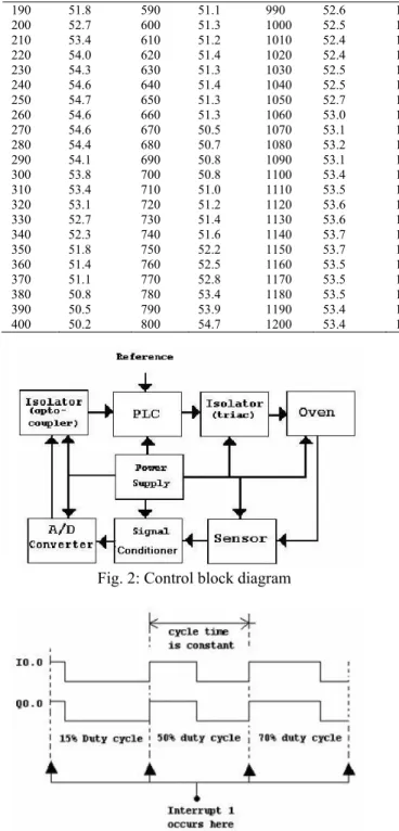
shown in Fig. 2.
The instantaneous temperature value is conveyed
by eight parallel lines connected to eight input points of
the PLC as given in Table 1.
Table 3: Temperature readings for proportional mode, Gain = 20% Time
[sec]
Temp. [C]
Time [sec]
Temp. [C]
Time [sec]
Temp. [C]
Time [sec]
Temp. [C]
Time [sec]
Temp. [C]
Time [sec]
Temp. [C] 10 29.3 410 47.3 810 46.7 1210 46.4 1610 46.2 2010 45.5 20 29.8 420 46.9 820 46.8 1220 46.4 1620 46.2 2020 45.4 30 31.9 430 46.5 830 46.8 1230 46.4 1630 46.2 2030 45.3 40 32.2 440 46.0 840 46.8 1240 46.4 1640 46.2 2040 45.2 50 33.0 450 45.5 850 46.8 1250 46.3 1650 41.8 2050 45.1 60 33.8 460 45.2 860 46.7 1260 46.3 1660 42.5 2060 44.9 70 34.6 470 44.2 870 46.6 1270 46.3 1670 43.6 2070 43.7 80 35.3 480 44.1 880 46.5 1280 46.3 1680 44.0 2080 43.8 90 36.4 490 44.1 890 46.4 1290 46.3 1690 44.5 2090 45.0 100 37.6 500 44.0 900 46.3 1300 46.3 1700 46.1 2100 45.3 110 38.7 510 44.6 910 45.8 1310 46.2 1710 46.9 2110 45.3 120 39.7 520 45.8 920 46.5 1320 46.1 1720 47.9 2120 45.1 130 40.8 530 46.4 930 45.5 1330 45.9 1730 48.3 2130 44.8 140 42.1 540 46.7 940 45.4 1340 45.6 1740 48.7 2140 44.6 150 43.3 550 46.9 950 45.3 1350 45.7 1750 49.3 2150 44.6 160 44.4 560 47.1 960 45.2 1360 45.9 1760 49.7 2160 44.6 170 45.6 570 47.2 970 45.4 1370 46.2 1770 49.9 2170 44.5 180 47.6 580 47.3 980 45.7 1380 46.2 1780 50.1 2180 44.5 190 48.4 590 47.3 990 46.3 1390 46.2 1790 50.2 2190 44.3 200 49.4 600 47.2 1000 46.5 1400 46.2 1800 50.2 2200 44.0 210 50.1 610 47.2 1010 46.6 1410 46.2 1810 50.2 2210 44.0 220 50.6 620 47.1 1020 46.6 1420 46.2 1820 50.1 2220 44.1 230 50.9 630 47.1 1030 46.6 1430 46.2 1830 50.0 2230 44.0 240 51.3 640 46.9 1040 46.5 1440 46.2 1840 49.9 2240 44.0 250 51.4 650 46.8 1050 46.6 1450 46.2 1850 49.8 2250 43.8 260 51.4 660 46.6 1060 46.4 1460 46.2 1860 49.7 2260 43.8 270 51.3 670 46.5 1070 46.3 1470 46.2 1870 49.5 2270 43.7 280 51.3 680 46.2 1080 46.1 1480 46.2 1880 49.2 2280 43.7 290 51.1 690 45.5 1090 45.8 1490 46.2 1890 49.0 2290 43.5 300 50.9 700 45.5 1100 45.6 1500 46.2 1900 48.8 2300 43.6 310 50.6 710 45.2 1110 45.4 1510 46.2 1910 48.6 2310 43.6 320 50.3 720 44.4 1120 45.3 1520 46.2 1920 48.5 2320 43.4 330 50.0 730 44.5 1130 45.4 1530 46.2 1930 48.2 2330 43.2 340 49.7 740 44.3 1140 45.6 1540 46.2 1940 48.0 2340 43.2 350 49.4 750 44.9 1150 46.2 1550 46.2 1950 47.7 2350 43.2 360 49.1 760 45.6 1160 46.3 1560 46.2 1960 47.6 2360 43.2 370 48.6 770 45.7 1170 46.3 1570 46.2 1970 47.4 2370 43.2 380 48.3 780 46.3 1180 46.4 1580 46.2 1980 46.3 2380 43.2 390 48.0 790 46.5 1190 46.4 1590 46.2 1990 45.5 2390 43.2 400 47.6 800 46.6 1200 46.4 1600 46.2 2000 45.6 2936 43.2
Table 4: Temperature readings for PI mode with disturbance Time
[sec]
Temp. [C] Time [sec]
Temp [C]
Time [sec]
Temp. [C] Time [sec]
Temp. [C] Time [sec]
Temp. [C] Time [sec]
Temp. [C]
190 51.8 590 51.1 990 52.6 1390 53.3 1790 51.9 2190 52.4 200 52.7 600 51.3 1000 52.5 1400 53.3 1800 52.5 2200 52.6 210 53.4 610 51.2 1010 52.4 1410 53.3 1810 53.4 2210 52.7 220 54.0 620 51.4 1020 52.4 1420 53.3 1820 54.5 2220 52.7 230 54.3 630 51.3 1030 52.5 1430 53.3 1830 55.0 2230 52.7 240 54.6 640 51.4 1040 52.5 1440 53.3 1840 56.0 2240 52.7 250 54.7 650 51.3 1050 52.7 1450 53.3 1850 56.7 2250 52.6 260 54.6 660 51.3 1060 53.0 1460 53.3 1860 58.0 2260 52.7 270 54.6 670 50.5 1070 53.1 1470 53.3 1870 58.3 2270 52.6 280 54.4 680 50.7 1080 53.2 1480 53.3 1880 58.3 2280 52.5 290 54.1 690 50.8 1090 53.1 1490 53.3 1890 58.0 2290 52.7 300 53.8 700 50.8 1100 53.4 1500 53.3 1900 57.5 2300 52.8 310 53.4 710 51.0 1110 53.5 1510 53.3 1910 57.1 2310 52.9 320 53.1 720 51.2 1120 53.6 1520 53.3 1920 56.7 2320 52.9 330 52.7 730 51.4 1130 53.6 1530 53.3 1930 56.1 2330 53.0 340 52.3 740 51.6 1140 53.7 1540 53.3 1940 55.6 2340 53.1 350 51.8 750 52.2 1150 53.7 1550 53.3 1950 55.0 2350 53.2 360 51.4 760 52.5 1160 53.5 1560 53.3 1960 54.5 2360 53.2 370 51.1 770 52.8 1170 53.5 1570 53.3 1970 53.4 2370 53.3 380 50.8 780 53.4 1180 53.5 1580 53.3 1980 53.1 2380 53.3 390 50.5 790 53.9 1190 53.4 1590 53.3 1990 52.1 2390 53.3 400 50.2 800 54.7 1200 53.4 1600 53.3 2000 52.4 2936 53.3
Fig. 2: Control block diagram
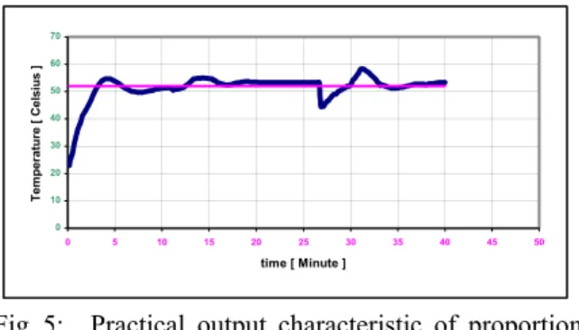
Fig. 3: PWM output timing diagram
undesirable jitter in the controlled variable synchronous
updates to the pulse width are realized by feeding back
the pulse output to the interrupt input point. By
enabling (attaching the event) the rising edge interrupt
of the input (I 0.0), PWM cycle is synchronized
[4], as
illustrated in Fig. 3.
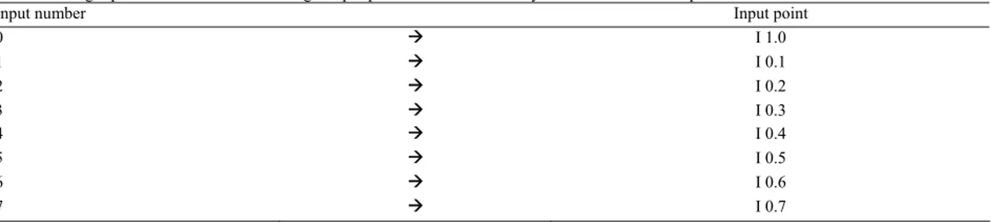
0 10 20 30 40 50 60
0 5 10 15 20 25 30 35 40 45 50
time [ Minute ]
Temperature [ Cel
s
iu
s ]
Fig. 4: Practical output characteristic of proportional
action with 20% gain
PLC program:
The Table 2 contains the PLC program
written in ladder diagram and statement list forms and
illustrated network by network. Important to note that
interrupts and subroutines are not parts of the main
program body. They function as independent units
when called.
EXPERIMENTAL RESULTS
0 10 20 30 40 50 60 70
0 5 10 15 20 25 30 35 40 45 50
time [ Minute ]
Tem
p
er
atur
e [ Celsius ]

![Table 3: Temperature readings for proportional mode, Gain = 20% Time [sec] Temp. [C] Time [sec] Temp](https://thumb-eu.123doks.com/thumbv2/123dok_br/18367804.354938/8.918.100.821.180.1068/table-temperature-readings-proportional-gain-time-temp-time.webp)