Hall Effect Measurements on p-n-p InP Structures
C. A. C. Sequeira and D. M. F. Santos
Department of Chemical and Biological Engineering, Instituto Superior T´ecnico, Technical University of Lisbon (TU Lisbon), Avenida Rovisco Pais 1, 1049-001 Lisboa, Portugal
Received on 7 November, 2007
The electrical properties of p-type layers of indium phosphide (InP), formed by the diffusion of zinc into n-type material, are studied by Hall Effect measurements. A wide range of diffusion conditions are used and both homogeneously doped specimens and those containing a zinc atom concentration gradient are produced. A non-correspondence of atom and carrier concentrations is indicated, confirming previous four point resistivity studies. Carrier profiles are achieved by both serial sectioning and multiple specimen techniques. Contacting procedures are developed from which plots of carrier mobility versus carrier concentration, in the range 5 x 10¹⁷ - 5 x 1019 cm−3, are produced for p-n-p InP. In the main, present results showed good reproducibility and conformed to the “rules” of the Van der Pauw technique.
Keywords: Indium phosphide; Zinc diffusion; Hall Effect measurements; Impurity profiles; Carrier mobility; Contacting procedures
I. INTRODUCTION
The formation of a p-type region in a previously n-type III-V compound semiconductor, by the indiffusion of diva-lent impurity atoms, is well known. The relationship between the number of introduced impurity atoms and the number of free carriers produced in the p-type region is dependent on the mechanism of diffusion and in particular on the position of the atoms when diffusion is complete.
One of the most studied of these materials is GaAs with Zn as the diffusant. An approximate “one to one” correlation between atom and carrier concentrations has been reported by many authors [1-10].
However, for the Zn/InP system, such a correlation has not been found. In our previous report [11], we discussed relevant previous work on InP, stressing that for high zinc concentra-tions, the number of free carriers does not match the number of introduced zinc atoms. Some preliminary studies involving p-n junction depth measurements have suggested a confirma-tion of this effect even at moderate doping levels.
Here, we briefly describe how this and other techniques have been extended to investigate the electrical properties of p-type layers formed by the diffusion of zinc into InP over a wide range of experimental conditions.
In the main, carrier concentrations and mobility values are found from a combination of resistivity and Hall Voltage mea-surements. The calculated concentrations from a measure-ment at a crystal surface only provide a true value for the whole layer if the crystal is uniformly doped. If this is not the case, then the value obtained is simply an average over the layer. The use of a serial sectioning technique with repeated measurements through the depth of the layer can lead to a car-rier profile with the aid of well established formulae. These re-late carrier concentrations to the properties of the layer before and after the removal of a section. Again, the values obtained will only be absolute for very small section thicknesses.
Four-point probe measurements on zinc diffused InP were described previously [11]. In this paper, we report Hall Effect measurements.
The main advantage of this method over the four-point probe is that from one single experiment, values of resistiv-ity, mobility and carrier concentration can be obtained.
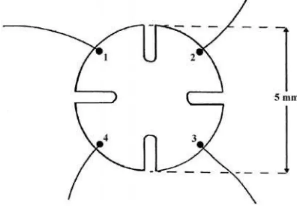
As explained in another paper [12], the most satisfactory method of carrying out the Hall Effect measurement is that due to Van der Pauw [13], using the “clover-leaf” specimen illustrated in Fig. 1. This type of specimen is used in all of this work.
FIG. 1: A “clover-leaf” Hall specimen.
II. CLOVER-LEAF PREPARATION
diffusion took place in a three-zone furnace accurate to±1 oC. The p-n junction was made visible by stain etching with KOH-K4[Fe(CN)6]-H2O solution (1:2:6, 1.0 s under intense illumination) and measured with a light microscope. The junction depths obtained varied from about 10 to 160µm. For a given set of experimental conditions, the junction lines fol-low the crystal contours; some of them are straight and flat, others are not flat, and some contain a small number of inclu-sions.
For the clover-leaf specimen preparation, following diffu-sion, the crystal of InP was removed from the ampoule and rinsed thoroughly with acetone. If the surface on which the initial measurements were to be taken was not the original dif-fused surface, then the crystal would, at this point, be etched back to the appropriate depth. Then it was fixed by one of its larger faces to a glass backing plate, using black wax. A mild steel mask cut into the desired clover-leaf design was then placed over the central region of the crystal and secured in place with a further quantity of black wax. The diameter of the mask was 0.5 cm. The completed assembly, then eas-ily handled using the glass plate, was then placed in an S.S. White Industrial Abrasive Unit. In this unit, the areas of wax and semiconductor not protected by the mask were removed using a mixture of 7µm diameter powder and air, directed un-der pressure through a fine nozzle. Careful manipulation of the nozzle produced a well defined specimen with little or no undercutting beneath the mask. The completed specimen was recovered from the assembly by dissolving away the remain-ing black wax in trichlorethylene. Since the edges of the origi-nal diffused crystal have been entirely removed by the blasting process, no problems are encountered due to the indiffusion of zinc at the side faces. The final clover leaf specimen is a per-fect p-n-p structure. Some care is necessary in the handling of these specimens to avoid the fracture of one or more of the four “leaves”.
III. POINT CONTACTING
The standard contacting technique that has been previously used by many workers is that of surface alloying. Such a technique was tried in this work and the procedure was fairly straightforward. All of the contacts were either of indium or an indium/zinc alloy. The contacting material was provided in wire form and the first step was to cut to small pieces the material from the wire. One piece was then moulded around the end of a short length (∼2 cm) of tinned copper wire and the process repeated four times. The four wires were then po-sitioned, with the indium pieces attached, on the top of the crystal as shown in Fig. 1, ready for alloying. The crystal itself sat on a hot plate inside a small bell jar through which gas could be passed (Fig. 2). With the wires in position, the jar was sealed down and the system flushed out thoroughly with nitrogen gas, for a period of several minutes. The nitro-gen was then diverted to flow through a bubbler containing concentrated hydrochloric acid. This provided a flow of N2
or three minutes, the hot plate temperature was increased to a point at which the contacting material just melted. At this point, there was a tendency for the indium to form a spherical blob on the surface, but a further increase of temperature to about 200-225oC generally caused the blob to collapse and wet the surface around the end of the wire. The temperature was maintained at this level for about 30 seconds and then the specimen was slowly cooled with a flow of pure N2. The pres-ence of HCl vapour in the gas flow, during alloying, helped in the breakdown of the spherical contact. The final contact was about 0.5 - 1 mm across its width.
FIG. 2: Rig for alloying contacts.
On n-type material this type of contact proved very success-ful and manufacture was relatively easy. However, for p-type material, the situation was different. The contacts were often found to be very brittle and easily broken away from the speci-men. Also, mechanically sound contacts had non-ohmic elec-trical characteristics, in general. On certain occasions a good set of contacts could be produced but the reproducibility fac-tor was poor. It has been found [14] that suitable contacts can be made to this type of material using indium/zinc alloys and a more sophisticated system of temperature control. There-fore, one can either use a better temperature programme or change to another system of contacting. The latter of these two alternatives was chosen here because of the type of exper-iment which was hoped to carry out. This was the production of an accurate carrier concentration profile again by a serial sectioning technique. Not only would alloyed contacts be dif-ficult to remove after measurement on each layer but also the chances of producing 4 good contacts on each of 10 layers, say, is small.
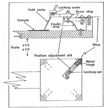
FIG. 3: Hall Effect jig for point contacting.
pressure contact or attached to the dots with colloidal silver paint.
The technique proved to be reasonably successful using in-dium or inin-dium/zinc dots on n-type material. Other contact materials or the use of p-type specimens led to nonohmic con-tacts and small values of current flow through the specimen. Some improvement was obtained by annealing the contacts but the method was eventually dropped for measurements on p-type material.
With the experience gained from the four-point probe work [11], a method of point contacting was tried. Such a method satisfies the requirements for easily removable contacts. A small jig (Fig. 3) was built, in order to accommodate the Van der Pauw specimens, with four probes in a square array.
Each probe was held in an independently sprung arm with position adjustment available to eliminate the need for exact specimen positioning. Initially, steel probes were used and gave a similar performance to that found in the earlier work. A switch to gold probes, however, gave an improved perfor-mance. For p-type material, “forming” was still necessary but could be achieved at a lower supply voltage (∼15 V). This and the inherently softer gold point led to less surface dam-age for each run. After each set of measurements, the probes could be simply lifted away from the specimen, which was then etched if required for a layer removal experiment and re-placed in the jig. Examples of the type of I-V characteristics found for this type of contact on p-type material before and af-ter “forming” are shown in Fig. 4. Typical contact resistances after “forming” were in the range 20-30Ω. In comparison, an I-V trace for a p-type sample using good alloyed contacts is also shown in Fig. 4.
The correspondence between the traces found for each type of contact is good. As an additional check on the effectiveness
sample carrier concentra-tion (1018cm−3)
carrier mobility (cm2V−1s−1)
radiotracer atomic level (1018cm−3)
atom / carrier ratio
700 2.3 39 60 26
900 3.5 26 300 85
750 9.5 30 170 18
carried out on three identically diffused specimens; two with point contacting and the other with alloyed contacts. The re-sults are given in Table I and are in good agreement for the values ofρ,nandµ(see Section IV). Consequently, the point contacting method would seem to be consistent and as good as the more often employed alloying technique. Thus, since it is also particularly suitable for use with successive layer removal, it is used for all of the Hall Effect measurements de-scribed in this work.
IV. EXPERIMENTAL PROCEDURE
After manufacture, the “clover–leaf” specimen was posi-tioned in the jig and the whole assembly placed between the poles of an electromagnet with the specimen surface parallel to the pole faces. Two locating points ensured that each spec-imen was positioned at exactly the same point within the pole gap. The contacts were then “formed” and their ohmic char-acteristic checked. The measuring sequence could then begin. As illustrated in Fig. 1, the coding 1, 2, 3, 4 is used for the different contacts described below. In the Van der Pauw technique, current is passed through the pairs of contacts 12, 23 and 13 in sequence; voltage measurements being taken across 34, 14 and 24, respectively, with no applied magnetic field. A field is then applied and the voltage across 24 re-measured, keeping the current through 13 constant. With no field,V34/I12(≡R1)andV14/I23(≡R2)are a measure of the specimen resistivity. In a perfect caseR1=R2. However, in practice, due to non-symmetry effects|R1−R2| is not zero but should equalR3 (≡ V24/I13)if the specimen is of uni-form character over its area. This equality condition provides a good check on the validity of each experimental run. Also, R1should be close toR2in value. A correction factor which is a function ofR1/R2may be applied, but high values ofR1/R2 should be suspected. Small cracks, for example, may lead to R1/R2being very large and the value of this ratio is again a good check of the experimental conditions. With a magnetic field appliedV24′ /I23′ ≡R3′and|V24′ −V24|is the Hall Voltage, VH.
In this work, for each of the contact pairings, eight separate voltage measurements were taken, the current remaining con-stant at 5 mA. This was achieved by using both directions of current flow, through 12 say, combined with a switch in polar-ity between 3 and 4 and then followed by a reversal of the roles of 12 and 34 with current through 34 and voltage across 12. This switching between sets of contacts and within the pair-ings was achieved efficiently by using two 6-way switches, linked such that a reading could only be taken if the correct
pairings were being used. If any of the contacts were not functioning correctly, it was apparent as a non-equality within the groups of eight readings. For a good experiment all eight readings were similar and an average value was taken.
From these values, the quantitiesR1andR2were calculated and further work continued only ifR1/R2was less than 1.25. The equality|R1−R2|=R3was also checked. A 5 % variation was acceptable. Using the Van der Pauw equation [12], the value of bulk resistivity was calculated as,
ρBulk= πb 2loge2
(R1+R2)f(R1/R2) (1) whereb is the sample thickness. For the case of a diffused layer with a p-n structure,bis taken as the junction depth since the junction provides a region of electrical insulation between the p and n regions. f(R1/R2)has been fully discussed in reference [12]. The sheet resistivity,ρs=ρB/b, whereρBis in units ofΩcm.
The magnetic field used in all of the work was 6 kG pro-duced by a magnet current of 4 A. The magnet was calibrated before starting the work. The residual magnetic field, with no current through the coils was 0.1 kG and had a negligible ef-fect on the “nofield” readings. The specimen was positioned between the poles at all times in order to cut down on the amount of specimen handling. The measurement of Hall Volt-age was carried out for both directions of the magnetic field and an average of the two values taken.
The Hall Voltage leads directly to a value of bulk Hall Coef-ficient,RH, and carrier concentration, p, using the equations,
RH=
VHb
IB (2)
and
p= (RHe)−1 (3)
whereBis the magnetic field andIthe specimen current.RH is measured in cm3C−1andpin cm−3.
The carrier mobility,µ, is found from,
µ= (peρB)−1 (4)
and is in units of cm2V−1s−1.
For the case of indiffused n-type specimens or homoge-neously doped p-type specimens the values of ρB, p(n)and
µ will be uniform throughout the depth of the specimen and thus the values calculated using equations (1) to (4) are correct at all points within the specimen and no further calculation is necessary. However, for the case of a diffused layer in which the carrier concentration and mobility are depth dependent, the calculated values of carrier concentration and mobility are weighted averages. For such a layer, an effective number of carriers per cm3,N
s, can be defined as
Ns= (ρBe µeff)−1 (5) withµeff=RH/ρB; the values of Hall Coefficient and bulk resistivity being measured at the top surface of the layer.
In order to eliminate such average parameters, Beuhler [15] devised a set of equations to calculate the values of p andµ in given layers of a diffused region from information gained from a combination of layer removal techniques and Hall measurements. His equations were,
(Rs)i (ρ2
s)i
−((Rρ2s)i+1 s)i+1
=eniµ2idi (6)
and
(ρs)−i 1−(ρs)i−+11=eniµidi (7) which give
µ i=
∆(Rs/ρ2
s)i
∆(1/ρs)i
(8)
and
n i=
∆(1/ρs)i
ediµi
(9)
whereRs (=RH/b)andρs(=ρB/b)are “sheet” parameters,
diis the thickness of theithlayer andΣdi=b(Rs)iand(ρs)i are the quantities found before the removal of theithlayer and ∆(Rs/ρ2
s)i, for example, is the change found in the parameter by the removal of theithlayer. From the results of this tech-nique, a quantity,Nd, for the average number of carriers per cm3can be calculated from,
Nd= 1
b
∑
nidi (10)In general, the quantitiesNdandNsdefined above will not be equal. This inequality between the two “average” terms arises because it is not strictly valid to apply the simple Hall Effect equations to the situation of one measurement on a dif-fused layer. Using these equations, µeff is RH/ρB and also (NseρB)−1. However, the latter of these terms is actually a
conductivity mobility (σ=neµσ)and Petritz [16] has shown that the conductivity mobility is weighted by the contribution of layers with higher mobility, in a diffused region, differently to the effective Hall mobilityRH/ρB. Therefore, the two ex-pressions forµeff will not actually be equal in practice, lead-ing toRH = (Nse)−1. ThusNs is not the true average value of carrier concentration as represented in an equation of the formR= (ne)−1. On the other hand,N
d is simply an aver-age value calculated from the true concentrations in individ-ual layers and thus is the true average concentration over the whole layer.Ndis generally greater thanNs. In terms of indi-vidual layers, Petritz showed that,
µeff=Rs/ρs=∑i
niµ2idi
∑iniµidi
(11)
whereas
µσ=
∑
i
niµidi
∑
i
nidi
(12)
Equations (6) to (9) were used to determine carrier profiles through several diffused specimens which contained atom concentration gradients.
For the initial experiments on homogeneously doped speci-mens, only one set of measurements for each side of the crys-tal was required. Reproducibility was checked by removing and replacing the specimen in the jig, with a different orienta-tion. When it was required to study a specimen with a concen-tration gradient, serial sectioning using chemical etching was employed. This procedure ran into difficulty because of the size and fragility of the Van der Pauw specimens. Even when the etching was done by hand on a polishing pad, breakages were commonplace. Also the small size of the samples led to non-flat etching, with the edges becoming rounded. Some good results were nevertheless obtained with some care. How-ever, it was decided to try and eliminate these problems by encasing the specimens in a resin block, with one face flush to the surface of the block. This should protect the specimen from breakage and also provide a large enough area around the specimen to stop non-parallel layer removal. Of course, in this case the sectioning cannot be accomplished by chemi-cal etching but must be done by mechanichemi-cal lapping. Unfortu-nately, this technique was not successful for two basic reasons. Firstly, many specimens suffered from the formation of hair-line cracks in the mounting procedure, caused by shrinkage of the resin. Also, it was difficult to assess the amount of ma-terial removed in lapping because of the imprecise nature of the block. Later the blocks were mounted in flat and parallel ended cylindrical metal mounts to provide uniformity. Fur-thermore, it was difficult to position the blocks in the mounts. A dial gauge was used to measure the thickness removed.
sample average resistivity, ρBulk(Ωcm)
average Hall Coeffi-cient,RH(cm3C−1)
average carrier concen-tration,p(cm−3)
average carrier mobility, µ(cm2V−1s−1)
time (min.)
H1 3.40 x 10⁻² 1.36 4.60 x 10¹⁸ 40 30
H2 3.07 x 10⁻² 1.20 5.20 x 10¹⁸ 39.2 30
H3 3.50 x 10⁻² 1.38 4.55 x 10¹⁸ 39.5 30
H4 4.72 x 10⁻² 2.00 3.13 x 10¹⁸ 42.3 90
surface (two for each specimen). The Van der Pauw speci-mens were then cut from the centre of the crystals to provide samples with good flat surfaces. Analysis of the experimental results was also carried out using the Beuhler equations [15] to provide a carrier profile.
FIG. 5: “Erfc” curve for diffusion of 30 minute duration at 750oC.
V. EXPERIMENTAL RESULTS
Preliminary experiments on “as received” n-type mater-ial gave results consistent with the information supplied by Thornton [17]. Carrier concentrations were in the range 6 x 1016cm−3to 1 x 1017cm−3. Mobility values were 3400-3600 cm2V−1s−1and bulk resistivity around 3 x 10²Ωcm. Both in-dium alloyed contacts and gold probes were used for several different samples. Annealing the n-type material for several hours at 750oC did not affect its electrical characteristics at all.
Homogeneously doped samples were prepared by long dif-fusions at 700oC, 750oC and 900oC, using a 1 mg Zn / 1 mg P source. The values of resistivity, mobility and carrier concentration as calculated from equations (1) to (4) are given in Table I. For comparison purposes, the corresponding tracer atomic concentration is lower than the atomic concentrations.
The ratios between the two parameters are 26, 18 and 85 for the 700, 750 and 900oC diffused specimens, respectively. The mobility values fall with increasing diffusion temperature and atomic concentration. The mobility of the carriers in p-type InP is seen to be low and a factor of about 100 lower than for electrons in n-type material.
FIG. 6: A carrier profile determined from Hall Effect measurements with serial sectioning. Also included are corresponding tracer pro-files, stain junction depths and background donor level.
radiotracer profile. Again a figure of 20 is a rough estimate of the atom/carrier ratio.
Better results were obtained under similar conditions but using a longer diffusion time of 90 minutes. With careful etch-ing, it was possible to produce a good set of results by suc-cessive layer removal. The thickness of each removed layer varied between 3 and 10µm. A typical example is H4 and the average values ofρB,pandµat the surface of this specimen are also given in Table II. They are very similar to those of the shorter time diffusions (H1, H2). Fig. 6 shows the carrier pro-file produced by using the calculations of Beuhler [15] on the sectioning and Hall measurements to giveni andµifor each layer. Also included is a corresponding “tracer profile”. This is in fact the curve of Fig. 5, now with a time factor of 2.45 (√6) applied.
This approximation of assuming an “erfc” form still is quite adequate for the purpose of comparison between atom and carrier levels. At all points, the carrier profile is below the “tracer curve”. A sharp peak in carrier concentration near the surface is followed in the bulk by a flat region of uniform con-centration at about 2-2.5 x 1018cm−3. The p-n junction, found by chemical staining, corresponds to an atomic concentration of 5 x 1017cm−3on the “tracer profile”. A plot of mobility versus concentration (µivs. ni)for this specimen is shown in Fig. 7. The mobility is seen to decrease with increasing con-centration. The effective or average mobility as measured at the original surface of the diffused layer is marked with an ar-row. Also plotted in this figure are the mobility values found for the homogeneously doped specimens. For H4, the effec-tive concentration valueNs is 3.13 x 1018 cm−3whereasNd is 4.18 x 1018cm−3. Nsis therefore about 75 % ofNd, a fig-ure similar to that found by Mayer [18] in implanted layers of silicon. For all of the p-type layers which were sectioned and probed at successive depths, the transition from p- to n-type material was found to correspond fairly closely (∼3 µm) to the position of the p-n junction as shown in the staining proce-dure. This is an important result since two completely differ-ent techniques are shown to be in agreemdiffer-ent on the position of the p-n junction. The reproducibility of results throughout this type of experiment was good.
From the experiment in which a number of nominally iden-tical samples were used (H5), in order to eliminate the need for sectioning between measurements, a form of analysis sim-ilar to that described above was used. Fig. 8 shows the cal-culated carrier profile and the corresponding “tracer profile” (H5T).
Again, an initial rapid fluctuation in carrier concentration is followed by a flattening out to approach a level of about 4 x 1018 cm−3. The mobility values are plotted in Fig. 7 to-gether with the average mobility as found at the original sur-face. The stained junction depth for these samples occurs at roughly 48µm corresponding to an atomic concentration of 9 x 1017cm−3(from measurements of p-n junction depths and radiotracer profiles not reported in this paper).
As an example, the tabulated results and calculation steps for a Hall (H4) experiment are shown in Table III.
FIG. 7: A plot of mobility versus concentration for the holes in zinc-diffused layers of p-type InP.
FIG. 8: A carrier profile determined from a multi-specimen Hall Effect experiment with a corresponding tracer profile. Also illus-trated are the errors involved in determining the concentration levels at stained junction positions.
VI. DISCUSSION
In all the experiments described in this paper, one feature of the experimental results is outstanding. This is the fact that in a diffused layer the number of electrically active carriers does not equal the total number of indiffused impurity atoms. The number of atoms is always the larger quantity.
thickness removed total layer, ∆x(µm)
profile pene-tration (µm)
b (µm)
ρB (102Ω cm)
RB (cm3 C−1)
ρs (Ω)
Rs (cm2 C−1)
ρs (Ω2)
ρ−s (Ω−1)
Rs/ρs (cm2 C−1Ω−2)
∆ρ−s (∆2)
∆Rs/ρs (∆1)
mobilityµ = ∆1/∆2 (cm2V−1 s−1)
1.6∆xµi (10−23)
carrier con-centration, ni(1023 cm−3)
plotted concen-tration (cm−3)
- - - 75 4.72 2.00 6.29 267 39.56 0.1580 6.75 - - -
-3 3 1.5 72 4.59 1.92 6.38 267 40.70 0.1567 6.56 22 0.19 86.364 414.55 0.0531 0.53
5 8 5.5 67 4.70 1.90 7.01 284 49.14 0.1426 5.78 141 0.78 55.319 442.55 0.3190 3.20
5 13 10.5 62 4.95 2.19 7.98 353 63.68 0.1253 5.54 173 0.24 13.872 110.976 1.5590 15.60
6 19 16.0 56 5.23 2.39 9.34 427 87.24 0.1071 4.89 182 0.65 35.714 342.850 0.5310 5.30
9 28 23.5 47 5.55 3.02 11.81 643 139.47 0.0847 4.61 224 0.28 12.500 180.00 1.2440 12.50
9 37 32.5 38 5.68 3.17 14.95 834 223.50 0.0669 3.73 178 0.88 49.438 711.91 0.2500 2.50
9 46 41.5 29 5.69 3.29 19.62 1134 384.94 0.0510 2.94 159 0.79 49.686 715.48 0.2220 2.20
11 57 51.5 18 5.06 3.36 28.11 1867 790.17 0.0356 2.36 154 0.58 37.662 662.85 0.2320 2.30
*stained junction at 75µm; quantities calculated using Beuhler’s equations (8) and (9).
and possible reasons for the observed discrepancy were fully discussed. Of course the same arguments apply to the Hall Effect study.
In conclusion to this section, it is worthwhile looking at the validity of the “one-carrier” type of analysis employed in the Hall Effect calculations. The use of this type of analysis can be open to some question when dealing with III-V com-pounds because of the large difference between the mobilities of electrons and holes found in these materials. For InP, for example,µe/µhis about 100. This kind of situation can lead to the electrons being the dominant species although existing in lower concentrations than the holes. As the “two-carrier” equation for Hall Coefficient,RH, demonstrates, a sample may appear n-type due to the multiplying factor (µe/µh)2when in factp>n. This equation is,
RH= 1 e
(p−nb2)
(p+nb)2 (13) whereb=µe/µh.
However, for the type of samples used in these experiments, the doping level is so high that the number of free electrons remaining in the p-type region is necessarily minor, according to the equation,
np=n2i (14)
The intrinsic carrier concentration,ni, for InP at room tem-perature is∼8 x 108cm−3. The only danger area for this ap-proach in diffused crystals with concentration gradients is in the regions for whichNais approximately equal toNd. Then the Fermi-Level is near to the centre of the forbidden gap and
n∼p∼ni (15)
In this situation, the dominant species would be determined by the mobility values. The regions over which this kind of condition will occur are very narrow and should not affect the bulk of the diffused region. For the previously described homogeneously doped specimens, of course,Nawill always be greater thanNd and the above situation will never arise. Therefore, the use of “one-carrier” equations is fully justified.
VII. CONCLUSION
Carrier profiles were obtained using Hall Effect techniques and a wide range of diffusion conditions. These measure-ments were found to be very satisfactory from an experimental point of view, providing several parameters with good repro-ducibility.
A typical carrier profile was shown in Fig. 6. After an ini-tial peak, the concentration is followed, away from the surface region, by a uniform level at about 22.5 x 1018cm−3; its p-n junction, found by chemical staining, corresponds to an impu-rity atom concentration of 5-6 x 1017cm−3.
For the multisample experiment, the same general shape of profile was found (Fig. 8) with a uniform level of 4 x 1018cm−3being approached. The stained junction depth cor-responds to 9.0 x 1017 cm−3 zinc atoms on the radiotracer profile.
For all of the diffused crystals which were sectioned and probed at successive depths, the transition from p- to n-type material corresponded fairly closely (∼ 3µm) to the position of the p-n junction as found by staining.
atom concentrations varied from 7 x 1019 cm−3(700oC) to 3 x 1020cm−3(900oC).
A combined plot of mobility versus carrier concentration for several specimens, including homogeneous doping, was
shown in Fig. 7. The general trend is for the mobility to de-crease with increasing concentration values. In our next paper on C-V measurements we revisit these matters.
[1] E. F. Schubert, Doping in III-V Semiconductors (Cambridge University Press, Cambridge, 2004).
[2] S. Adachi,Properties of Group-IV, III-V and II-VI Semiconduc-tors(Wiley, New York, 2005).
[3] B. Tuck, J. Cryst. Growth208, 123 (2000).
[4] J. Decobert, D. Herrati, V. Colson, D. Leclerc, and L. Goldstein, J. Cryst. Growth248, 390 (2003).
[5] K. M. Yu and M. C. Ridgway, Nucl. Instrum. Meth. B168, 65 (2000).
[6] Y. W. Zhao, Z. Y. Dong, and C. J. Li, J. Cryst. Growth275, 381 (2005).
[7] M. O. Manasreh,InP and Related Compounds: Materials, Ap-plications and Devices(Wiley, New York, 2000).
[8] S. Aytac¸ and A. Schlachetzki, Solid-State Electron. 24, 57 (1981).
[9] R. L. Causley and R. A. Lewis, Physica B302-303, 327 (2001).
[10] E. H. Rhoderick, III-Vs Review13, 45 (2000).
[11] C. A. C. Sequeira and D. M. F. Santos, Braz. J. Phys.39, 1077 (2007).
[12] C. A. C. Sequeira and D. M. F. Santos, Czech J. Phys.56, 549 (2006).
[13] L. J. Van der Pauw, Phillips Research Report13, 1 (1958). [14] R. Jakiela, A. Barcz, E. Wegner, and A. Zagojski, Vacuum78,
417 (2005).
[15] M. G. Beuhler, Stanford Research Report, SEL-66-064 (1966). [16] R. L. Petritz, Phys. Rev.110, 1254 (1958).
[17] P. R. Thornton, The Physics of Electroluminescence Devices (Spon, London, 1967).