Brazilian Journal of Physics, vol. 34, no. 2B, June, 2004 669
Electronic Properties of Isolated Nickel in Diamond
R. Larico
†, J. F. Justo
‡, W. V. M. Machado
†, and L. V. C. Assali
†,
†
Instituto de F´ısica, Universidade de S˜ao Paulo, CP 66318, 05315-970, S˜ao Paulo, SP, Brazil
‡
Escola Polit´ecnica, Universidade de S˜ao Paulo, CP 61548, CEP 05424-970, S˜ao Paulo, SP, Brazil
Received on 31 March, 2003
Isolated nickel impurities in diamond have been investigated using the spin-polarized full-potential linearized augmented plane wave total energy method. The electronic and atomic structures, symmetries, transition en-ergies, and formation energies of substitutional and interstitial Ni impurities in diamond were computed. The results were discussed in the context of the electrically active centers in synthetic diamond.
1
Introduction
Synthetic diamond is generally grown by high pressure-high temperature methods using transition metals alloys (contain-ing manganese, iron, nickel, and cobalt) as catalysts. Nickel, which is incorporated into the resulting diamond crystal, has been unambiguously related to a large number of electri-cally and optielectri-cally active centers. Electron paramagnetic resonance (EPR) and optical absorption measurements have shown that these centers are either related to isolated Ni [1, 2, 3] or to Ni-dopant complexes [4]. Some absorption lines are stronger under high nitrogen concentrations, while others are stronger under low nitrogen concentrations. Al-though some nickel-nitrogen complexes could be formed [4], nitrogen will only shift the Fermi level of the system, activating or deactivating a certain isolated nickel center[5]. As a result of intensive experimental investigations, a microscopic model has been built for the interactions of Ni with the diamond crystalline lattice. Nickel has a 3d84s2
atomic valence configuration, which will hybridize with nearest-neighboring carbon atoms in the host crystal. Inter-stitial nickel was identified in the positive charge state (Ni+i ) with a spin 1/2 in trigonal or tetrahedral symmetry [2, 3]. Substitutional nickel was identified in the negative charge state (Ni−
s) with a tetrahedral symmetry and a spin 3/2 [1]. Previous theoretical investigations of Ni in diamond has been restricted to calculations using small cluster models [6, 7], in which atomic relaxations have not been considered. However, as it will be shown latter, relaxations play a ma-jor role on the electronic properties of those Ni-related de-fects. Here, we used the full-potential linearized augmented plane wave (FP-LAPW) method [8, 9], implemented into the WIEN97 package [10], to investigate the electronic and structural properties of nickel-related defects in diamond. Our results are discussed in the context of the experimentally identified electrically active centers in synthetic diamond.
2
Methodology
We used total energy methods to investigate the substi-tutional and interstitial Ni impurities in diamond. The
calculations were performed within the density functional theory [11], combined with the Perdew-Burke-Ernzerhof exchange-correlation potential [12]. In the FP-LAPW framework, two distinct regions are defined inside the sim-ulation cell: the spherical atomic regions and an interstitial region. In the later, the electronic wave-functions were ex-panded in a plane-wave basis set, with a cutoff depending on the choice of the atomic sphere radii. For bulk diamond, a convergence in the total energy was achieved by using 7.0/R (maximum length of the plane-waves), where R is the small-est radius of the spheres defining the host atoms. We used small atomic radii (RC= RNi= 1.2 a.u.), as opposed to larger
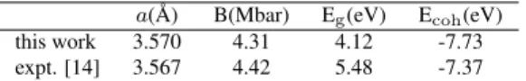
atomic radii with touching spheres (R = 1.46 a.u. in the equilibrium lattice constant). This choice would allow large relaxations on the internal degrees of freedom without any atomic sphere overlap. In the atomic regions, we used a spherical harmonic basis set with azimuthal quantum num-ber up toℓ=10 and a non-spherical contribution up toℓns=4. The carbon 1s and the nickel 1s, 2s, and 2p atomic wave-functions were treated as core states. The Brillouin zone (BZ) was sampled by a 6× 6 ×6 grid of k-points [13], which is reduced to 16k-points in the irreducible BZ (IBZ) for the primitive cell. Self-consistent interactions were per-formed until convergence on both the total energy (10−4eV per unit cell) and total charge in the atomic spheres (10−5 electronic charges per atom) was achieved. Table I presents the theoretical results of crystalline diamond compared to the experimental data [14].
The electronic structure of Ni impurities in diamond was studied by considering a 54-atom reference supercell and a 2×2×2 grid [13], corresponding to a unique point to in-tegrate in the IBZ. The convergence criteria were the same as the ones described earlier. The atomic positions were re-laxed until the forces were smaller than 0.05 eV/ ˚A.
Table I: Theoretical structural and electronic properties of diamond: lattice constant (a), bulk modulus (B), energy band gap (Eg), and cohesive energy
(Ecoh).
a( ˚A) B(Mbar) Eg(eV) Ecoh(eV)
670 R. Laricoet al.
3
Isolated Ni defects
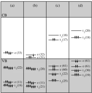
Figure 1 displays the impurity energy levels for the tetrahe-dral interstitial Ni (in neutral and positive charge states) and the substitutional Ni (in neutral and negative charge states) centers around theΓpoint.
The neutral interstitial nickel center in diamond (Ni0 i),
shown in fig. 1(a), presents a closed shell structure with a fully occupied e level in the band gap and has a Td
symme-try. The Tdcrystal field splitting of 1.8 eV splits the Ni
3d-related energy levels into a t2plus an e level, the former
be-ing resonant in the valence band. This behavior is similar to the neutral interstitial Ni impurity in silicon [15]. The nickel nearest-neighbor and next-nearest-neighbor atoms undergo outward relaxations of 0.28 ˚A and 0.11 ˚A, respectively. This center in a positive charge state (Ni+i ) and in a Tdpoint
sym-metry, shown in fig 1(b), has an effective spin of 1/2. For the positive charge state, the crystal field splitting is essen-tially the same as the one for the neutral charge state. On the other hand, the exchange splitting (∆Exc) acts mostly over
the gap energy level with e symmetry, being about 0.15 eV. This effect drives the center to a low spin configuration. The electronic structure of the Ni+i center is fully consistent with the microscopic model proposed to explain the EPR signals of synthetic diamond grown from a Ni-solvent with the ad-dition of a nitrogen getter [2].
The neutral substitutional nickel center in a Td point
symmetry (Ni0
s) in diamond, shown in fig. 1(c), presents
an effective spin S=1. The Tdcrystal field of 3.2 eV splits
the Ni 3d-related energy levels into an e plus a t2level, the
former being resonant in the valence band. The exchange splitting acts over all levels, being ∆Exc(e) = 0.3 eV and
∆Exc(t2) = 0.6 eV, driving the center to a low spin
config-uration. The configuration of Ni0
s in diamond is similar to
the theoretical result of the same center in silicon, which also gives an effective spin S=1 [15]. The nickel nearest-neighbor atoms undergo an outward relaxation of 0.23 ˚A. This center presents small distortions which are not shown in the figure.
The substitutional nickel center in negative charge state (Ni−
s), shown in fig. 1(d), has a Td point symmetry and
presents an effective spin S=3/2. The Tdcrystal field of 3.7
eV splits the Ni 3d-related energy levels into an e plus a t2
level, the former being resonant in the valence band. The ex-change splitting acts over all levels, being∆Exc(e) = 0.5 eV
and∆Exc(t2) = 0.9 eV, driving the center to a low spin
con-figuration. The nickel nearest-neighbor atoms undergo an outward relaxation of 0.23 ˚A, very similar to the relaxation for this center in the neutral charge state.
4
Formation and transition energies
The formation energy of a Ni impurity in a q charge state, (∆Efq) is given by
∆Eqf = E(nC,nNi,q)−nCµC−nNiµNi+ q (µe+εv),
(1)
t (19) e (11) t (22) e (33)
t (21) e (11) t (20) e (31) e (32)
t (25) t (22) e (60) e (61) t (17) t (18)
t (19) t (30) e (61) e (61) t (18) t (20)
2 2
2 2
2 2 2 2
2 2 2 2
VB CB
(a) (b) (c) (d)
Fig. 1. The Kohn-Sham energy eigenvalues representing the Ni 3d-related impurity levels near the gap region: (a) Ni0i, (b) Ni
+ i ,
(c) Ni0
s, and (d) Ni−s centers. The level occupation is given by the
number of↑(spin up) and↓(spin down) arrows, respectively. The percentage of Ni 3d-character of the energy levels inside the atomic spheres are represented by the numbers in parenthesis. The figure only displays those energy levels which are related to the Ni impu-rity, as computed by the charge percentage with d character. VB and CB symbols represent the valence and conduction bands.
where E(nC,nNi,q)is the total energy of a supercell
calcu-lation withnCcarbon atoms andnNiNi atoms, andµCand
µNiare the chemical potentials for C in a diamond structure
and Ni in a fcc structure, respectively. The electron chemi-cal potentialµedefines the Fermi level position in the band
gap (with respect to the top of the valence band,εv).
The computed formation energy (∆Ef) of the
intersti-tial nickel, in neutral charge state, is 8.7 eV higher than the energy of the substitutional nickel in the same charge state. Based only in formation energy considerations, sub-stitutional nickel is considerably more favorable than inter-stitial nickel. Using the total energies of the centers in pos-itive and negative charge states, we computed the transition energies. The acceptor transition energy (-/0) of the Nisis
εv+ 2.9 eV, which is in excellent agreement with the
exper-imental data ofεv + 3.0 eV [16, 17]. The donor transition
energy (0/+) of the Niiis computed to beεv+ 0.5 eV.
5
Summary
In summary, we performed an investigation on the electronic and structural properties of isolated nickel impurities in di-amond. For most of the nickel centers studied here, our results are fully consistent with proposed models based on the EPR and optical experiments on synthetically grown di-amond. Additionally, the computed acceptor transition en-ergy for the Nis center is in agreement with experimental
Brazilian Journal of Physics, vol. 34, no. 2B, June, 2004 671
Acknowledgments
This work was supported by Brazilian agencies FAPESP and CNPq. The calculations were performed at the LCCA-CCE of the Universidade de S˜ao Paulo.
References
[1] J. Isoya, H. Kanda, J. R. Norris, J. Tang, and M. K. Bowman, Phys. Rev. B41, 3905 (1990).
[2] J. Isoya, H. Kanda, Y. Uchida, Phys. Rev. B42, 9843 (1990).
[3] M. H. Nazar´e, A. J. Neves, and G. Davies, Phys. Rev. B43, 14196 (1991).
[4] S. C. Lawson and H. Kanda, J. Appl. Phys.73, 3967 (1993).
[5] G. Davies, Phyica B273-274, 15 (1999).
[6] Y. Jinlong, Z. Manhong, and W. Kelin, Phys. Rev B49, 15525 (1994).
[7] J. Goss, A. Resende, R. Jones, S. ¨Oberg, and P. R. Briddon, Mater. Sci. Forum196-201, 67 (1995).
[8] P. Blaha, K. Schwarz, and P. Sorantin, Comput. Phys. Com-mun.59, 399 (1990).
[9] D. J. Singh, Planewaves, Pseudopotentials and the LAPW method(Kluver Academic, Norwell, 1994).
[10] P. Blaha, K. Schwarz, and J. Luitz,WIEN97,A Full Potential Linearized Augmented Plane Wave Package for Calculating Crystal Properties(Karlheinz Schwarz, Techn. Universitatat Wien, Austria), 1999.
[11] P. Hohenberg and W. Kohn, Phys. Rev.136, B864 (1964).
[12] J. P. Perdew, S. Burke, and M. Ernzerhof, Phys. Rev. Lett.77, 3865 (1996).
[13] H. J. Monkhorst and J. D. Pack, Phys. Rev. B13, 5188 (1976).
[14] Landolt-B¨ornstein,Numerial Data and Functional Relation-ships in Science and Technology, vol. 17, edited by O. Madelung, M. Schulz, and H. Weiss (Springer-Verlag, New York, 1982).
[15] F. Beeler, O. K. Andersen, and M. Scheffler, Phys. Rev. B41, 1603 (1990).
[16] D. M. Hofmann, P. Christmann, D. Volm, K. Pressel, L. Pereira, L. Santos, and E. Pereira, Mater. Sci. Forum 196-201, 79 (1995).