Universidade de Aveiro 2016
Departamento de Eletrónica, Telecomunicações e Informática
Guilherme Marieiro
Cabral
TRANSFORMADA DE HAAR BASEADA EM ÓTICA
INTEGRADA
ALL OPTICAL HAAR TRANSFORM BASED ON
PLANAR WAVEGUIDES
Universidade de Aveiro 2016
Departamento de Eletrónica, Telecomunicações e Informática
Guilherme Marieiro
Cabral
ALL OPTICAL HAAR TRANSFORM BASED ON
PLANAR WAVEGUIDES
Dissertação apresentada à Universidade de Aveiro para cumprimento dos requisitos necessários à obtenção do grau de Mestre em Engenharia Electrónica e Telecomunicações, realizada sob a orientação científica do Dr. António Teixeira e Dr. Mário Lima, Professores do Departamento de Electrónica Telecomunicações e Informática da Universidade de Aveiro
This work is funded by Fundação para a Ciência e a Tecnologia (FCT) under the project “COMPRESS- All-optical data compression” – PTDC/EEI-TEL/7163/2014
Dedico este trabalho aos meus pais e à minha irmã por me ajudarem a alcançar os meus objectivos e à minha namorada pelo apoio e dedicação durante esta jornada.
o júri
presidente / president Professor Doutor José Rodrigues Ferreira da Rocha
Professor Catedrático da Universidade de Aveiro
vogais / examiner committee Professor Doutor Paulo Sérgio de Brito André
Professor Associado com agregação da Universidade de Lisboa
Professor Doutor Mário José Neves de Lima
agradecimentos Encerrando assim esta etapa, não poderia deixar de salientar as pessoas que, de uma forma ou outra, contribuíram para a concretização do meu projeto. Ao Prof. Dr. António Teixeira e ao Prof. Dr. Mário Lima por me orientarem ao longo desta jornada que sempre com boa disposição me acompanharam, permitindo-me assim chegar à meta.
Ao grupo de ótica do Instituto de Telecomunicações pela camaradagem e vontade de resolver os problemas que foram surgindo.
Aos amigos de longa data só tenho a agradecer o facto de nos termos conhecido naquele dia e podermos agora partilhar tão boas e caricatas histórias que me alegram todos os dias.
Ao Francisco, o meu profundo obrigado pela partilha da vasta sabedoria, permanente disponibilidade e amizade.
À Andreia por ter sido a motivação em pessoa e me fazer sentir especial todos os dias.
E por fim, à minha família pelo apoio inigualável, carinho e compreensão. Com eles fui aprendendo a levantar-me sempre que “caí”.
palavras-chave MMI, PIC, Processamento ótico de imagem, Transformada de Haar
resumo Com o constante evoluir das necessidades do ser humano nos últimos anos, a
transmissão e armazenamento de dados para aplicações vídeo e media têm crescido exponencialmente, obrigando a uma procura incessante de novas soluções para optimizar a largura de banda. Com a finalidade de obter um processamento de imagem mais rápido, os métodos de compressão são uma importante ferramenta para reduzir os dados redundantes. Entre diversas técnicas de transformação para compressão, as transformadas baseadas em wavelets são as mais usadas devido à sua simplicidade e computação rápida. Relativamente a esta abordagem, dadas as suas vantagens, o processamento de imagem totalmente ótico é aqui realizado, sendo baseado na transformada de Haar. Dado que esta transformada de wavelet já provou os seus benefícios face a outros métodos de transformação para compressão, a sua implementação em estruturas óticas guiadas é obrigatória.
Neste contexto, é introduzido Photonic Integrated Circuit (PIC), já que pode incluir vários componentes num único chip ótico. Entre a extensa lista de blocos de construção (BBs) disponíveis para esta integração fotónica, as estruturas de interferência multimodo (MMI) são apresentadas como solução para realizar a transformada ótica de Haar.
O desenvolvimento de tal componente foi elaborado assim como a sua implementação num PIC, concretizando a transformada de Haar de primeira ordem. Utilizando os BBs de uma fábrica específica, o esquemático do circuito de uma solução adoptada foi também implementado.
keywords Haar Transform, MMI, Optical image processing, PIC
abstract With the evolution of the human needs in the last years, data transmission and
storage for video and media applications have grown exponentially, demanding the search of new solutions for optimizing the bandwidth. In order to have faster image processing, compression methods are fundamental tools to decrease the redundant data. Among several transformation techniques for compression, wavelet-based transforms are the trendiest ones because of its simplicity and fast computation.
Concerning this approach and given the advantages, all-optical image processing is here performed based on Haar Transform. Since this wavelet transform has shown its benefits when compared to other methods, its implementation in optical guided structures is mandatory.
In this context, Photonic Integrated Circuit (PIC) is introduced since it can include different components into a single optical chip. Between the extensive list of building blocks (BBs) available for this photonic integration, the Multimode Interference (MMI) structure is presented as a possible solution to perform the optical Haar wavelet transform.
The development of such a structure was done likewise its implementation into a PIC, performing the first order Haar. Using the BBs from a specific foundry, a layout of the circuit from an adapted Haar Transform solution was also made.
TABLE OF CONTENTS
TABLE OF CONTENTS ... 1 LIST OF FIGURES ... 2 LIST OF TABLES ... 4 LIST OF ACRONYMS ... 5 1. INTRODUCTION ... 71.1 Context and Motivation ... 7
1.2 Objectives ... 10
1.3 Structure ... 10
1.4 Contributions ... 12
2. HAAR TRANSFORM ... 13
2.1 Introduction ... 13
2.2 Haar transform - image processing and compression ... 15
2.3 Optical Haar transform approach ... 17
2.4 Haar transform coupler design ... 18
3. MULTIMODE INTERFERENCE ... 21
3.1 Multimode Waveguides ... 21
3.2 Propagation Constants and Working principle ... 22
3.3 General Interference MMI ... 24
3.4 Restricted Interference MMI ... 26
3.4.1 Paired Interference ... 27
3.4.2 Symmetric Interference ... 28
4. MMI COUPLER APPLIED TO HAAR TRANSFORM AND RESULTS ... 29
4.1 Introduction ... 29
4.2 Haar transform based in Waveguides ... 30
4.3 Haar transform based in Waveguides and Phase shifter ... 32
4.4 Haar transform modeling ... 33
4.4.1 8X8 MMI Coupler Configuration ... 33
4.4.2 2x2 MMI Coupler with Phase Shifters Configuration ... 38
5. MMI Design and Implementation ... 41
5.1 Foundry introduction ... 41
5.2 8x8 MMI Coupler Design ... 43
5.3 8X8 MMI Coupler Implementation ... 48
5.4 2X2 MMI Coupler Implementation ... 49
6. CONCLUSIONS AND FUTURE WORK ... 51
Appendix A ... 54
Appendix B ... 55
LIST OF FIGURES
Figure 1.1 Development of applications market enabled by ASPICS [9] ... 9
Figure 2.1 Sub-band decomposition using wavelet transform ... 14
Figure 2.2 Image processing and compression base on Haar optical wavelet transform (OWT) [12] ... 15
Figure 2.3 3D basic module for 1st level HT of 2x2 data matrix [19] ... 17
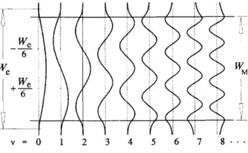
Figure 3.1 Schematic view of a 2x2 multimode interference (MMI) coupler. Light from the input waveguide is launched into the MMI section, propagated, and imaged into the output waveguides. [27] ... 21
Figure 3.2 Example of amplitude-normalized lateral field profiles ψv(y), corresponding to the first 9 guided modes in a step-index multimode waveguide [23] ... 22
Figure 3.3 MMI section with length LN produces N images of the extended input function fin(x) [27] ... 23
Figure 4.1 Phase difference between ports for Haar Transform ... 29
Figure 4.2 First order Haar wavelet filter using a 2x2 GI MMI Table 4.5 Phase difference between ports ... 33
Figure 4.3 Setup of 8x8 MMI coupler to obtain Haar transform ... 34
Figure 4.4 Field power spatial distribution of 8x8 MMI coupler ... 35
Figure 4.5 Field power vertical slices of 8x8 MMI coupler ... 35
Figure 4.6 Input phase sweep (both ports) vs. Output power for 8x8 MMI coupler ... 37
Figure 4.7 Input phase difference (one port only) vs. Output power for 8x8 MMI coupler ... 38
Figure 4.8 Setup of 2x2 MMI coupler to obtain Haar transform ... 38
Figure 4.9 Input phase sweep (both ports) vs. Output power for 2x2 MMI coupler system ... 40
Figure 4.10 Input phase difference (one port only) vs. Output power for 2x2 MMI coupler system . 40 Figure 5.1 Measured waveguide propagation losses for TE and TM propagation [29] ... 42
Figure 5.9 Photonic integrated circuit mask for 1st order HT ... 49
Figure B.1 MMI 8x8 Field Power Vertical Slices acting as splitter 1:8 ... 55
Figure B.2 MMI 8x8 Field Power Spatial Distribution acting as splitter 1:8 (input@port1) ... 55
Figure B.3 MMI 8x8 Field Power Spatial Distribution acting as splitter 1:8 (input@port2) ... 56
Figure B.4 MMI 8x8 Field Power Spatial Distribution acting as splitter 1:8 (input@port3) ... 56
Figure B.5 MMI 8x8 Field Power Spatial Distribution acting as splitter 1:8 (input@port4) ... 57
Figure B.6 MMI 8x8 Field Power Spatial Distribution acting as splitter 1:8 (input@port5) ... 57
Figure B.7 MMI 8x8 Field Power Spatial Distribution acting as splitter 1:8 (input@port6) ... 58
Figure B.8 MMI 8x8 Field Power Spatial Distribution acting as splitter 1:8 (input@port7) ... 58
LIST OF TABLES
Table 3.1 Summary of characteristics of the General and Restricted Interference [8] ... 26
Table 4.1 Phase difference in degrees between ports for symmetric interference mechanism (1x2 MMI (a), 1x3 MMI (b) and 1x4 MMI (c) respectively) ... 30
Table 4.2 Phase difference in degrees between ports for paired interference mechanism (2x2 MMI (a), 2x3 MMI (b) and 2x4 MMI (c) respectively) ... 30
Table 4.3 Phase difference in degrees between ports for general interference mechanism (2x2 MMI (a), 3x3 MMI (b), 4x4 MMI (c), 5x5 MMI (d) and 6x6 MMI (e) respectively) ... 31
Table 4.4 Phase difference in degrees between ports for 8x8 General Interference MMI ... 32
Table 4.5 Phase difference between ports……….30
Table 4.6 Phase difference between ports for 8x8 MMI coupler simulated in VPIphotonics™ at Lπ=0,375 ... 36
Table 4.7 Output power measures from modeled 8x8 MMI coupler ... 37
Table 4.8 Output power measures from modeled 2x2 MMI coupler system ... 39
LIST OF ACRONYMS
1D One Dimension2D Two Dimension
ASPIC Application Specific Photonic IC BB Building block
BPM Beam Propagation Method
CMOS Complementary Metal-Oxide-Semiconductor CMT Coupled Theory Mode
DC Direct Current
DCT Discrete Cosine Transform DFT Discrete Fourier Transform DRC Design Rule Check
DWT Discrete Wavelet Transforms e-o Electro-Optical
FhG-HHI Fraunhofer-Gesellschaft - Heinrich-Hertz-Institut FMM Film Mode Matching
GDS Graphic Database System GI General Interference
HP High Pass HT Haar Transform IC Integrated Circuit
InGaAsP Indium Gallium Arsenide Phosphide InP Indium Phosphide
JePPIX Joint European Platform for InP-based Photonic Integration of Components and Circuits JPEG Joint Photographic Experts Group
LP Low Pass
MMI Multimode Interference
MPA Guided Modal Propagation Analysis MPW Multi-Project Wafer
MSE Mean Square Error
PARADIGM Photonic Advanced Research and Development for Integrated Generic Manufacturing PDK Process Design Kits
PSNR Peak Signal-to-Noise Ratio oeo Optical-to-Electronic-to-Optical OWT Optical Wavelet Transform PIC Photonic Integrated Circuits R&D Research and Development Si Silicon
SSC Spot-Size Converter TE Transverse Electric TM Transverse Magnetic VPA Virtual Power Analyzers
1. INTRODUCTION
1.1 Context and Motivation
The reason why all-optical networks become so attractive was purely the desire to eliminate or reduce the number of expensive and power consuming optical-to-electronic-to-optical (oeo) conversions in microelectronics integrated circuits (ICs), by performing some part of the process in the optical domain. Photonic integrated circuits (PIC) have its first appearance in 1969, where the future of microphotonic integration was described by P.Tien [1] as “the integration of a large number of optical devices in a small substrate, so forming an optical circuit reminiscent of the integrated circuit in microelectronics”.
Comparatively to ICs in microelectronics, these planar lightwave circuits provide many of the same advantages including low cost per device and per functionality, low power loss, higher reliability and due to low power requirement a low operating cost. Also the similarities of both conceptions are clear since it is possible to integrate a huge variety of optical components such as modulators, detectors, attenuators, multiplexers, optical amplifiers and lasers as it is in electronics.
Likewise electronics, photonic integration can be largely divided into two groups, hybrid and monolithic integration.
Hybrid integration refers to the case where the discrete devices involved are usually bonded together into a single package. However, this approach can be highly complex due to the fact discrete devices must be interconnected and optical alignment has to be assured bringing less reliability. Also because of different packaging designs due their optical and thermal characteristics the cost of production will also increase [2].
As an alternative, monolithic integration involves multiple devices that are fabricated in the same material substrate generating a single “chip” and package. This approach solves the package consolidation and also the promise of increasing network functionality. Also due the single photonic material yielding, optical connections and fiber couplings are no longer a major problem and the power
consumption and space are reduced. Therefore, for an optical solution monolithic integration has better characteristics than hybrid [3].
Considering the available primary host materials for monolithic photonic integration, silicon (Si) and indium phosphide (InP) are the market leaders choice.
The first one brings a return of the research and development (R&D) invested in electronic ICs. Given this multi-billionaire industry and the knowledge from CMOS technology, a promise for enabling both optical and electronic integration is assured. Using a silicon substrate leads to a good performance which is achieved from lower propagation loss and also component dimensions and power dissipation reduced. Although these advantages may seem attractive, contrary to InP which is a flagship material for light source, with Si substrate it is only possible the integration of passive optical devices due to some difficulties with implementation of electro-optical (e-o) functions such as lasing, modulation and light detection [4][5].
Since Si membrane is limited for higher circuit complexities due to the lack of on-chip light generation and amplification, operating in the optical telecommunication wavelengths, InP is proven to be the best solution. According to Meint Smit et al. [6] due to achieving e-o and all-optical information control, this substrate brings a reliable integration with different functionalities not only passive but also active functions such as wavelength multiplexing, demultiplexing, variable optical attenuation, switching, dispersion, lasing, amplification and modulation. Also when compared to other substrates, InP is the one where multi-project wafer runs (MPW) offer more functionalities at lower cost and process design kits (PDK) have a more powerful components libraries than others with open access [7].
Concerning generic photonic integration, photonic design foundries started to develop in Europe by 2008 [8].
Figure 1.1 Development of applications market enabled by ASPICS [9]
PIC manufacture can be divided in two parts: design and fabrication. For designing these “chips”, one have the so called fabless companies where PICs are designed according the rules and ready to use building blocks (BBs) available from foundries for application specific photonic IC (ASPICs) [10]. Later in fabrication process, MPW access is offered at least once a year through consortiums like JePPIX (Joint European Platform for InP-based Photonic Integration of Components and Circuits) [7]. This association is where InP and TriPleX™ based PICs present themselves to the photonics community. It has been supported by several and mostly European universities and companies which are cooperating and putting some effort to build a generic foundry technology infrastructure. The goal of this platform is the low-cost development of ASPICs using generic foundry model and supply design kits for MPWs. For this purpose the program PARADIGM [11] was designed due interest in universities to get access to foundry processes given their cooperation with companies that will generate later commercial designs. The aim was also reducing the costs of design, development and manufacture through establishing library-based design combined with technology process flows and design tools.
As one can conclude from Figure 1.1, ASPICs design interest has been increasing through years exceeding one billion Euro before 2020, making InP a growing and innovative industry.
Given the demanding for data transmission and storage nowadays, compression is becoming an important field of study and several techniques are emerging in order to release more bandwidth. Among others, the trendiest ones are the wavelet-based transforms due to their fast computation and efficiency [15].
In order to implement such kind of compression method to images and taking into account the reliability of such structure, an all-optical network is the best solution. By applying this architecture into a PIC, the advantages sort out because image compression can be done with fewer costs associated, more power saving and also faster due to an all-optical processing [12].
1.2 Objectives
Given the context and motivation presented, using the efficiency and robustness of PICs, optical image processing is the main goal of this thesis. Therefore, the following objectives are:
• Study of all-optical image processing system
• Present an alternative for the optical wavelet transform (OWT) adiabatic coupler
• Simulation of first order Haar wavelet transform • Design of a multimode interference (MMI) coupler
• Design implementation of a solution for a specific foundry • Present the on-chip layout solutions
1.3 Structure
• MMI design and implementation • Conclusion and Future work
The first chapter is written to present the framework, objectives and structure of this dissertation and also the contributions provided.
In the second chapter it is presented an overview of the Haar wavelet transform in order to study image processing. Concerning this compression method, an analysis of a provided solution consisting of an all-optical architecture was also made. Focusing on its Haar optical wavelet transform approach, an investigation was done for the purpose of finding a new solution.
The third chapter is an exposition about multimode interference couplers where the concept and working principle is descripted. Also it is presented the propagation constants and equations that allow the construction of a self-imaging mechanism according to its category.
In chapter four, simulations of the MMI coupler are applied to perform the Haar wavelet transform. In this section new solutions were presented and simulations were given in order to validate the performance of the Haar Transform (HT) using software VPIphotonics™.
The fifth chapter, a brief introduction to the foundry used is done and design and implementation of the architectures are set using PhoeniX Software™. The first solution was adapted from literature and a layout was performed, the other was a new all passive scheme solution where the coupler was designed and later implemented.
At the end, the sixth chapter concerns the appreciation of the work done and it also includes a possible future work to develop in this research area.
1.4 Contributions
The main contributions that this work provides are the follow:
• Overview of the solution provided from Giorgia Parca et al. [12] • Simulation of an adapted and new solution for the first order HT • Design of an 8x8 MMI that performs the first order HT
• Schematic layouts for a specific foundry
• G.Cabral, F. Rodrigues, M. Lima and A. Teixeira “Photonic Integrated Haar Function” proceedings for XIII Symposium on Enabling Optical Networks and Sensors
2. HAAR TRANSFORM
2.1 Introduction
In a digital point of view, an image can be seen has a group of pixels. This statement brings the fact that neighboring pixels are correlated and usually redundant. Given the rapidly growth of communications and video-media applications, one needs to decrease this redundancy to optimize the transmission speed and the bandwidth of the system and by applying compression techniques to those images one can do this enhancement. There are several ways to achieve signal compression in digital signal processing but frequently the most usual transforms are based on orthogonal functions. In multi-resolution analysis an important property is the orthogonality, which stands by the original signal to be split into a low and high frequency part enabling the splitting without duplicating information. These functions, only requires subtractions and additions for their forward and inverse transforms and as example can be: Discrete Fourier Transform (DFT), Discrete Cosine Transform (DCT), Discrete Wavelet Transforms (DWT) [13]. These last ones, gives many advantages, since they represent a fundamental tool for local spectral decomposition and nonstationary signal analysis, which are used in the JPEG2000 standard as wavelet-based compression algorithms [14] .
Wavelets provide an efficient means for approximating continuous functions, and depending on the design criteria, such as smoothness or accuracy of approximation, an optimal wavelet basis is important to be set. Between the extensive variety of wavelet-based, the Haar wavelet transform seems to fit perfectly for image processing and pattern recognition due to its low computing requirements (memory efficient), easy implementation by optical planar interferometry, best performance in terms of computation time and efficient compression method [15][16]. Also, this type of transform is extremely useful in applications where real time implementation of edge detection is required [17].
The Discrete wavelet transforms can represent an image as a sum of wavelet functions, by taking the signal into a set of detail and approximate coefficients. Known as Daubechies D2 wavelet, the Haar wavelet transform, which matrix is given by
Equation 2.1, has the capability of acquire low pass and high pass behaviors of an image and it can be done as a fast algorithm, which is quite important for the considered image compression.
Haar transformation matrix
𝐻 =
! ! ! ! ! !−
! !Since the purpose of this thesis is to apply to 2D signals, like images, wavelet decomposition needs to be understood. This decomposition, Figure 2.1, is made by applying it to an image, the original one, and getting as a result sub-images which have inferior resolution and corresponding different frequency bands. To make this wavelet decomposition it is required to have two filters: a low-pass filter LP and a high-pass filter HP. The reason of this LP filter is to do an approximation of the image itself and the HP is to get the high frequency information. This filtering operation practically corresponds to the calculation of the average between two neighbor pixels values (low-pass) or the difference between them (high-pass) [12].
• Low-pass filter 𝐿 (𝑛) = !! ! !!!!!
• High-pass filter 𝐻 (𝑛) = !!!!!!!!
For starting, with input data matrix N x N, it is applied on the rows both low pass and high pass filters and the result consists in two different matrices, L and H which contains the horizontal approximation and the horizontal detail respectively. Next, on these subsequent matrices it is applied once again both LP and HP filters to its columns, and four different matrices are obtained: 𝐿𝐿, 𝐿𝐻, 𝐻𝐿 and 𝐻𝐻. The first one corresponds to the average of the original matrix while the other ones are the details (vertical, horizontal and diagonal). This wavelet decomposition was also performed in MATLAB®, in Appendix section A, for better understanding of this multi-resolution analysis. It was used a square image since the Haar wavelet transform requires it.
The Haar wavelet transform is the accomplishment after this decomposition however it is possible to achieve higher-level transforms by repeating the same decomposition method [18]. The reconstruction to obtain the original image it is possible without losses if no quantization is applied, which means one can have lossless image compression with Haar transform.
2.2 Haar transform - image processing and compression
In an all-optical scheme, it was reported a solution in [12] and [19] that is built on blocks and can be used for image processing. This established system can be verified in Figure 2.2
Composed by four main blocks, with this system one can achieve the desired fast image processing.
The first building block is the optical sensors array, which is responsible for light detection at input, where the 2D data is going to be acquired. After the sampling, this procedure leads to an N x N matrix ready for the next step.
The following block is the Haar optical wavelet transform that is in charge for applying the decomposition transform, with the respective Haar low-pass and high-pass filters, to the data according to the described in the previous chapter. It is considered in Equation 2.2, the N x N matrix and the corresponding scattering matrix for a generic 1D input (ai coefficients). The resulting coefficients after applying the
filters (low-pass and high-pass) twice are the scaling cij and detail dij coefficients
(being i the transform level and j the coefficient index). Since the considered input data is a two-dimensional matrix, this process needs to be applied twice, one for the horizontal component and then for the vertical one.
⋮ 𝑐!" 𝑑!" 𝑐!! 𝑑!! 𝑐!" 𝑑!" ⋮ = 1 2 ⋮ 1 1 0 1 −1 0 0 0 1 0 0 0 0 0 0 1 0 0 0 0 1 0 0 0 0 0 0 −1 0 0 0 1 1 0 1 −1 ⋮ ⋮ 𝑎! 𝑎! 𝑎! 𝑎! 𝑎! 𝑎! ⋮ Eq. 2.2
Subsequently in the chain, the compression block is responsible, besides to compress, for the extraction from the 2D wavelet transform. Its purpose is the quantization and the selection of the desired sub-band component as the 𝐿𝐿 in Figure 2.2, which represents the approximated image (scaling).
can reconstruct the original image since one of the properties of the transform is perfect reconstruction. [20]
2.3 Optical Haar transform approach
Assuming the purpose of this compression system is designed for image processing, two-dimension input must be taken into account, which means that must be built a three-dimension coupler based network [19], capable to perform the desired operations. With a 2𝑥2 matrix as an input (corresponding coefficients a0, a1, a2 and a3
from Equation 2.2), when applied the scattering Haar matrix, the result are the detail and scaling coefficients from the horizontal dimension. As discussed before, this network is responsible for applying the filters in two stages, so this operation needs to be repeated once more to accomplish the vertical dimension. At the end, scaling cij
and detail dij are created, where i is the filtering step on each dimension and j the
coefficient index [12].
Figure 2.3 3D basic module for 1st level HT of 2x2 data matrix [19]
It is also stated [12] the possibility of increasing the data input matrix by iterating and pilling the module in Figure 2.3 thus reaching a 2nd level Haar Transform. However, this module-composed structure was considered for lossy compression techniques, which means there will be some discarded data in the compression stage bringing to inverse transform processing less information. Given the human visual sensitivity for low-frequency components instead for high frequency, this spotted characteristic made the compression possible without losing too much quality at one’s
eyes. So, by providing more relevance to low-frequency and discarding the other components in the optical Haar transform system, at the compression stage it was only selected the 𝐿𝐿 sub-band level.
Making a comparative study of this lossy technique, considering a 𝑁𝑥𝑁 input image, it was involved another method of compression [12]. For matching the 1st level Haar wavelet transform, the image was divided in 4 sub matrices and then for the comparison with the 2nd level Haar wavelet transform the original matrix was divided in 16 sub matrices. This method was based in the subtraction of a pixel over the others in the matrix and image quality assessment parameters such as Mean Square Error (MSE) and Peak Signal to Noise Ratio (PSNR) were taken as comparison. MSE is a parameter where evaluates the difference between an obtained value and the true value of the pixel obtained. It measures the average of the square error and closer the value is to 0, more similar to the original is the compressed one. PSNR is another parameter used for image quality assessment, where the square of the peak value in the image is taken and divided by the MSE. From the MATLAB® environment it was stated that with these two techniques, the performance decreases with increasing compression however the optical system with Haar transform offers higher image manipulation capability and potential. [12]
2.4 Haar transform coupler design
Based in 3 𝑑𝐵 asymmetric couplers, an optical approach was reported [12][21]. Such couplers, also known as Magic-T, allow the achievement of the Haar transform since the reproduced matrix matches perfectly with the filters that perform in HT. With this implementation it is possible to realize the needed mathematical operations, difference and average between both optical inputs.
50% of the waveguides and optimized for the output waves to be in phase when the input is the wider waveguide and to have a 𝜋 phase difference when the input is the narrower waveguide. These phase relations correspond to the Haar mathematical operations of sum and difference respectively [22].
Even though the good performance of this system composed by asymmetric couplers, an improvement can be done in the OWT.
Since MMI couplers have compact and robust size, low cross-talk, low power imbalance and also when compared with adiabatic couplers better extinction ratio. MMI structures have also the advantage of ease of fabrication and less sensitive to fabrication tolerences ratio, proving that they can be a good alternative.
3. MULTIMODE INTERFERENCE
3.1 Multimode Waveguides
Founded on the self-imaging principle of periodic objects illuminated by coherent light, [23] by which an input field profile is reproduced in single or multiple images at periodic intervals along the propagation direction of the guide one can have the working principle of an MMI. The self-imaging property of a multimode waveguide is due to the interference of the waveguide modes which are excited by the object. Therefore, when the superposition of the modal fields in the image plane is the same as the object plane, the self-image is formed. A full-modal propagation analysis (MPA) provides an analytical theory that describes the self-imaging phenomena in a multimode waveguide [23].
MMI devices, as the one in Figure 3.1, have innumerous applications either as component (power splitters [24], 90º hybrid couplers [23]) or based devices (optical switches [25], phased array multiplexers [26]) and many benefits like their compact size, high tolerance to fabrication process and large optical bandwidth.
Figure 3.1 Schematic view of a 2x2 multimode interference (MMI) coupler. Light from the input waveguide is launched into the MMI section, propagated, and imaged into the output waveguides. [27]
3.2 Propagation Constants and Working principle
To comprehend how the MMI block operates, one needs to study the concept beneath the propagation of multimode waveguide when light interference occurs.
Having demonstrated that the waveguide comprises a ridge and cladding with an effective refractive indices, correspondingly 𝑛! and 𝑛! and a width 𝑊! at a free-space wavelength 𝜆!, 𝑚 lateral modes are propagated with mode numbers 𝑣 =
0, 1, . . . (𝑚 − 1), as in Figure 3.2.
Figure 3.2 Example of amplitude-normalized lateral field profiles 𝝍𝒗(𝒚), corresponding to the first 9 guided modes in a step-index multimode waveguide [23]
There is also a relationship between the ridge index and the propagation constant 𝛽! and the lateral wavenumber 𝑘!𝑣, which is done by the dispersion
equation [23],
general way, waveguides have high-contrast. The propagation constant of each mode can now be determined as [23],
𝛽! ≃ 𝑘!𝑛!−(𝑣 + 1)!𝜋𝜆! 4𝑛!𝑊!!
Eq. 3.2
Also with great use to operate MMIs, the beat length, which is the distance between the two lowest-order mode and is defined by 𝐿! [23]
𝐿! = 𝜋 𝛽! − 𝛽! ≃
4𝑛!𝑊!!
3𝜆! Eq. 3.3
Which result in the characterization of the propagation constants spacing [23]
(𝛽! − 𝛽!) ≃ 𝑣(𝑣 + 2)𝜋
3𝐿! Eq. 3.4
To comprehend where the mirrored images are placed alongside the waveguide, it is used the analytic perspective MPA by decomposing the input field into modal field distributions.
At a distance 𝑧 one can write the field as [23]
Ψ(𝑦, 𝑧) = 𝑐!𝜓!(𝑦) 𝑒!(!"!!!!) !!!
!!!
Eq. 3.5
Since the phase is a common factor to all modes (𝜔𝑡 − 𝛽!𝑧) = (𝛽!− 𝛽!) 𝑧 and assuming the field time dependent, at 𝑧 = 𝐿
Ψ(𝑦, 𝐿) = 𝑐!𝜓!(𝑦) 𝑒!!(!!!)!!!! !
!!!
!!!
Eq. 3.6
Taking in consideration this equation, if one extracts the exponential factor, it is possible to obtain the mode phase factor, which together with the modal excitation 𝑐! makes dependent the diversity of images formed. These images can be categorized in two different self-imaging mechanisms: General Interference and Restricted Interference.
3.3 General Interference MMI
General Interference (GI) MMIs are based on mechanisms that are not dependent on modal excitation. The types of images formed are only dependent on the mode phase factor.
exp [ 𝑗𝜈 𝜈 + 2 𝜋
spacing is going to be 0, which will lead to a direct replica due to the fact all the modes have the same relative phase.
The second condition is related to changing the phase alternatively between odd and even integer multiples of 𝜋. Since the even resultant modes will be in phase, the main difference between this state and the previous one consists only on the odd modes, which will result in a mirrored single image. Therefore, this leads to the conclusion that direct and mirrored single images of the input field will occur at a distance even or odd integer multiples of length 3 𝐿!.
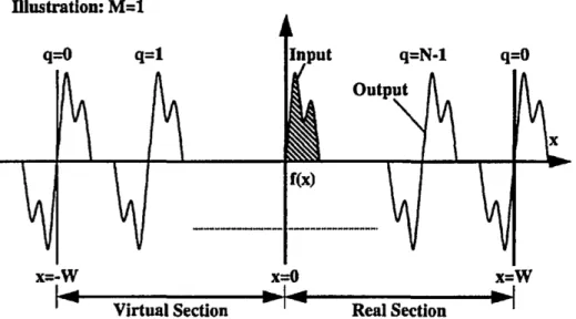
Still concerning about the periodicity of the mode phase factor, multiple images will also occur along the waveguide between single images. Due to the Eigenmode decomposition of the input and making a numerical mode analysis, it is then applied an extension of the real MMI section called virtual MMI section for mathematical simplicity [27]. Using then a special Fourier decomposition to the Eigenmode decomposition of the input field distribution one can deduce that N images are obtained at distances [23]
𝐿 = 𝑝
𝑁 (3 𝐿!) Eq. 3.8
where 𝑝 ≥ 0 𝑎𝑛𝑑 𝑁 ≥ 1 are integers with no common divisor other than 1.
Since positions, phases, and amplitudes of multiple images are not quite obvious with the eigenmode superposition output field, it is then used an output distribution with multiple images of the input [27].
Ψ y, L = 1 𝐶 Ψ!" 𝑦 − 𝑦! 𝑒 𝑗𝜑𝑞 !!! !!! Eq. 3.9 𝑦! = 𝑝(2𝑞 − 𝑁) 𝑊! 𝑁 Eq. 3.10 𝜑! = 𝑝(𝑁 − 𝑞)𝑞𝜋 𝑁 Eq. 3.11
Where 𝐶, a complex normalization constant such that |𝐶| = √𝑁, a sum of 𝑁 images along 𝑦 numbered by 𝑞 and 𝑝 is referring to imaging periodicity along 𝑧. Using these previous equations, one can achieve the relative phases and also the positions of the images at the output ports, which can be very convenient for designing MMIs. Given this, it is possible to conclude that multiple self-imaging mechanism allows the design of NxN and NxM optical couplers and since this phenomenon is periodic it is relevant for shorter devices that p is equal to 1 [23].
For the purpose of design a general interference coupler, it should be regarded the relative phase of an imaging input 𝑟 = 1, 2, … 𝑁 to an output 𝑠 = 1, 2, … 𝑁
𝜑!" =
𝜋
4𝑁 𝑠 − 𝑟 2𝑁 + 𝑟 − 𝑠 + 𝜋 , 𝑓𝑜𝑟 (𝑟 + 𝑠) 𝑒𝑣𝑒𝑛 Eq. 3.12
𝜑!" = 𝜋
4𝑁 𝑟 + 𝑠 − 1 2𝑁 − 𝑟 − 𝑠 + 1 , 𝑓𝑜𝑟(𝑟 + 𝑠)𝑜𝑑𝑑 Eq. 3.13
3.4 Restricted Interference MMI
To self-imaging mechanisms that are acquired by exciting only some particular guided modes in the waveguides it is called Restricted Interference. With this interference mode, one can build shorter specific MMIs than with GI-MMI. It can be divided according the periodicities of mode phase factor in two different categories: paired interference and symmetric interference [23]. To resume the main characteristics of the possible types of interference, the table 3.1 is presented.
Interference Mechanism General Paired Symmetric
Inputs x Outputs 𝑁 𝑥 𝑁 2 𝑥 𝑁 1 𝑥 𝑁 First single image distance 3 𝐿! 𝐿! 3 𝐿!
3.4.1 Paired Interference
In this selective excitation of modes, one can reduce the length periodicity with a factor of three [23],
𝑚𝑜𝑑! = 𝑣 𝑣 + 2 = 0 , for 𝜐 ≠ 2, 5, 8, … Eq. 3.14
That means that single image representations, direct replicas or mirrored images, will be shown at 𝐿 = 𝑝(𝐿!), with 𝑝 = 0, 1, 2, … Concerning multiple images, in this special case of two-fold images, these can be found at 𝐿 =!!(𝐿!), with 𝑝 = 𝑜𝑑𝑑 , which leads the formation of N-fold images at
𝐿 = 𝑝
𝑁 𝐿! Eq. 3.15
with 𝑝 ≥ 0 𝑎𝑛𝑑 𝑁 ≥ 1 integers without common divisor other than 1.
These conclusions are based on the fact the input field Ψ(y, 0) is launched at positions 𝑦 = ±!!!, where modes that are not excited present a zero with odd symmetry [23].
To reach this interference mechanism, the correspondent excited modes are paired and when the properties stated above are achieved (Equation 3.14), one can observe that each even mode leads its odd partner by a phase difference of !! at 3 𝑑𝐵 length, 𝑧 = !!!.
According to the purpose of the mechanism, for designing multimode interference coupler also matters the phase relation between input and output ports, and it can be found depending on the input upper arm and input lower arm respectively [24].
𝜑! = 𝜑!+ !!! 𝑠 2𝑁 + 2 − 3𝑠 , for 𝑠 𝑜𝑑𝑑 Eq. 3.16
𝜑! = 𝜑!+ !!! 2𝑠 − 3𝑠! − !
! 𝑁 − 2 , for 𝑠 𝑜𝑑𝑑 Eq. 3.18
𝜑! = 𝜑!+ !!! 4𝑠 − 3𝑠!− 1 − !! 𝑁 − 2 + 𝜋, for 𝑠 𝑒𝑣𝑒𝑛 Eq 3.19
where 𝜑! denotes a constant phase
3.4.2 Symmetric Interference
Even though it is possible to build 1-to-N splitters according general interference (Equation 3.8), regarding this selective excitation mechanism, if one only excites the even symmetric modes of the waveguide, the result is a length periodicity four times shorter.
𝑚𝑜𝑑! = 𝑣 𝑣 + 2 = 0, for 𝜐 = 𝑒𝑣𝑒𝑛 Eq. 3.20
When input field Ψ(y, 0) is launched at 𝑦 = 0 and the Equation 3.20 is verified, by linear combinations of the even symmetric modes, single images will appear at 𝐿 = 𝑝 (!!!
! ), with 𝑝 = 0, 1, 2, … which leads the creation of N-fold images at [23],
𝐿 = 𝑝 𝑁 (
3𝐿!
4 ) Eq. 3.21
with 𝑁 images spaced by !!!
According to Bachmann et al. [24] to design this kind of mechanism, relative phase relation of the images between input and output should be regarded as
4. MMI COUPLER APPLIED TO HAAR TRANSFORM AND
RESULTS
4.1 Introduction
With the purpose of finding a suitable solution for implementing the Optical Haar Transform, several optic components such as couplers and MMIs were studied and after a deep research based on previous work, one can find it possible using MMIs.
Looking carefully to the main goal, it is possible to assume that the phase difference between output and input are the key to have a successful Haar Transform.
Figure 4.1 Phase difference between ports for Haar Transform
Concerning the work made by Giorgia Parca et. al [12], to achieve the 𝜋@3𝑑𝐵 condition, mathematical operations need to be respected. In Figure 4.1 it is possible to observe the same considerations but instead the usage of a coupler, the construction of this model is based on a multimode interference coupler where the sum (upper output arm) and subtraction (lower output arm) depends on the MMI used. Concerning Figure 4.1, it is supposed an a and b as input field and the expected is in one of the outputs a phase difference of 0 (sum) and in another output a phase difference of 𝜋 (subtraction).
GENERAL MMI a b ½ [ a[0°] + b[0°] ] ½ [ a[0°] + b[180°] ] or ½ [ a[180°] + b[0°] ]
(a) (b) (c)
(b) (a)
4.2 Haar transform based in Waveguides
After some investigation on different categories of MMIs, using equations 3.[12,13,16,17,18,19,22] that concerns to phase relation from the previous chapter, a MATLAB® script was made to find out possible solutions that match the requirements for design an All-Optical Haar Transform. The presented following tables are related to the phase difference between the input and output ports and these are numbered from top to bottom (input) and left to right (output) from 1 to 𝑁.
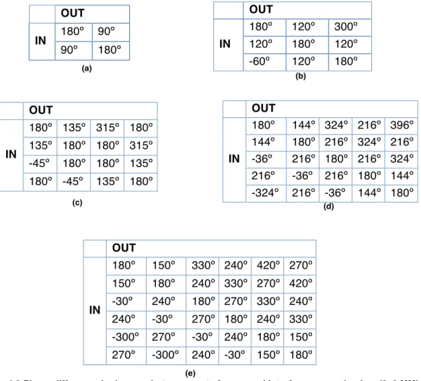
Table 4.1 Phase difference in degrees between ports for symmetric interference mechanism (1x2 MMI (a), 1x3 MMI (b) and 1x4 MMI (c) respectively)
Starting the research with use of a symmetric interference mechanism, it is clear to understand that is impossible to construct the desired since as one can see in Table 4.1 (a) there is no phase difference between the outputs and in (b) and (c) it is also noticeable that this difference doesn’t match with the 𝜋 required to fulfill the Haar theory.
OUT IN 0º 90º 90º 0º OUT IN 0º 0º OUT IN 0º 60º 0º OUT IN 75º 15º -45º -60º 60º -360º OUT IN 67,5º -22,5º -22,5º 67,5º OUT IN 78,75º 33,75º 33,75º -101,25º -101,25º 33,75º -326,25º -281,25º
(a)
(b)
(e)
(c) (d)
configurations made with the paired interference couplers returns an equivalent phase relation as the desired one.
By managing these results, there was no need to iterate the next cases of configuration (more outputs) due to restricted interference couplers mathematical operations, thus leading the impossibility to design a MMI of this category that satisfies completely the Haar transform condition. Given this, further study was made within general interference mechanism characteristics.
Table 4.3 Phase difference in degrees between ports for general interference mechanism (2x2 MMI (a), 3x3 MMI (b), 4x4 MMI (c), 5x5 MMI (d) and 6x6 MMI (e) respectively)
By analyzing Table 4.3 it is possible to perceive again, as in restricted interference, that all these configurations cannot be implemented as a desired solution, however, one can deduce the possibility of finding a solution that solves the Haar transform since there is some evidence of the phase relation needed.
OUT IN 180º 120º 300º 120º 180º 120º -60º 120º 180º OUT IN 180º 90º 90º 180º OUT IN 180º 144º 324º 216º 396º 144º 180º 216º 324º 216º -36º 216º 180º 216º 324º 216º -36º 216º 180º 144º -324º 216º -36º 144º 180º OUT IN 180º 135º 315º 180º 135º 180º 180º 315º -45º 180º 180º 135º 180º -45º 135º 180º OUT IN 180º 150º 330º 240º 420º 270º 150º 180º 240º 330º 270º 420º -30º 240º 180º 270º 330º 240º 240º -30º 270º 180º 240º 330º -300º 270º -30º 240º 180º 150º 270º -300º 240º -30º 150º 180º
Table 4.4 Phase difference in degrees between ports for 8x8 General Interference MMI
Following the deep investigation about the different types of multimode interference couplers, a solution that matches with a possible optical Haar approach came up. In the Table 4.4 it is possible to recognize this ability to the 8x8 MMI block, where with an input field at ports 1 and 4 it is produced the desired output. For instance, at output port 3, one can observe that both input signals have the same phase (sum) and at output port 7 the signals have a 𝜋 phase difference (subtraction), which is the main principle for Haar transform operation.
4.3 Haar transform based in Waveguides and Phase shifter
Although the interest into an all-passive solution for signal processing is greater, the one presented by Trung-Thanh Le [28] based on passive planar devices and phase shifters is also quite attractive. The benefit comparatively to the 8x8 MMI block is the small number of input/output waveguides which when becomes larger, the intrinsic propagation constant error, that is responsible for the bad uniformity to the output power, cannot be neglected [31]. And also as an advantage, the BBs used for
OUT IN 180º 157,5º 337,5º 270º 450º 337,5º 517,5º 360º 157,5º 180º 270º 337,5º 337,5º 450º 360º 517,5º -22,5º 270º 180º 337,5º 337,5º 360º 450º 337,5º 270º -22,5º 337,5º 180º 360º 337,5º 337,5º 450º -270º 337,5º -22,5º 360º 180º 337,5º 337,5º 270º 337,5º -270º 360º -22,5º 337,5º 180º 270º 337,5º -562,5º 360º -270º 337,5º -22,5º 270º 180º 157,5º 360º -562,5º 337,5º -270º 270º -22,5º 157,5º 180º
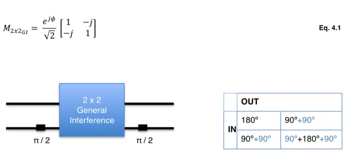
𝑀!!!!" = 𝑒!" 2
1 −𝑗
−𝑗 1 Eq. 4.1
Figure 4.2 First order Haar wavelet filter using a 2x2 GI MMI Table 4.5 Phase difference between ports According to the representation of Figure 4.2 and given the results in Table 4.5, when added phase shifters at input and output of these MMIs, one can observe the phase relation needed to reach a first order Haar wavelet filter (a sum and a subtraction at the output arms of the building block).
4.4 Haar transform modeling
In order to obtain the first order Haar wavelet filter, the software VPIphotonics™ was used. This commercial photonic simulator provides powerful tools that allow the characterization of both solutions stated above such as the use of its native modules and modeling the existing MMI block.
4.4.1 8X8 MMI Coupler Configuration
Based in literature it was seen that is possible to realize the first order Haar transform with MMI structure. In order to prove that, with help of VPIphotonics™ software, one can study the behavior of the coupler.
By changing the parameters from the MMI block to the requested ones, such as 8 inputs/outputs, design frequency for 𝜆=1550 𝑛𝑚 and others, a first experiment was made for better understanding.
At first instance, the structure used was an MMI 8x8 giving the input power only at one port (first), which means this block will behave as a splitter 1x8. From the
OUT IN 180º 90º+90º 90º+90º 90º+180º+90º 2 x 2 General Interference π / 2 π / 2
spatial distribution (Figure B.2 in Appendix B) one can observe the power at the first input port and spreading through the waveguide into the 8 output ports. The normalized length of this block was also based in Soldano and Pennings [23] Equation 3.8 for general interference, showing that at 𝑧 =!! 𝐿! the first eight-fold images will appear. This performance can also be proved from the Vertical Slices (figure B.1 in Attachments) where all the 8 outputs ports at this length have a uniform power distribution.
In order to prove the possibility of implementing this mechanism, the input field was also changed to the other input ports and the result was consistent with the first experiment (Figures B.3-B.9 in Appendix B). It was also conducted a test to comprehend the performance of this splitter where the input power was 1 𝑚𝑊 and changing to each input port, the results obtained in Table B.1 (Appendix B) matches the expected output of 0,125 𝑚𝑊 per port in every single case.
Given the coupler was totally adjusted and matches the expected behavior further tests were made to prove the Haar compatibility.
Figure 4.3 Setup of 8x8 MMI coupler to obtain Haar transform
To accomplish the principle of the wavelet transform, as noted in Table 4.4, the input signal should be added into ports 1 and 4, being seen the results in ports 3 and
𝑧 = !! 𝐿! the power is expectable to be less noticeable than the beginning due to the
ratio of this setup, which is 1: 8. The good performance of this device is shown at Figure 4.5 where the Vertical slices demonstrate the veracity of the mathematical operations at the output. From right to left, the ports are numbered 1 to 7, and given that both lasers have the same frequency, 𝑎 and 𝑏 have the same power. It is now clear that at port 3 the maximum output power corresponds to an addition and at port 7 the result is null power, behaving as a subtraction.
Figure 4.4 Field power spatial distribution of 8x8 MMI coupler
Also to sustain the thesis of this full optical solution for Haar transform, the Table 4.6, which is also resultant from the simulator, demonstrates that the phase relation addressed in theory are the same, no phase difference between outputs waveguides in output port 3 and 180° degrees phase difference between outputs in output port 7.
Table 4.6 Phase difference between ports for 8x8 MMI coupler simulated in VPIphotonics™ at Lπ=0,375
To understand if these mathematical operations were fully formulated with this coupler, a feasible solution was the measurement of power. With the help of power analyzers (VPA) blocks were placed at desired input and output ports.
For studying the correct performance of the OWT with this setup, it was applied an input power of 1 𝑚𝑊 into each of the continuous wave lasers, having both the same frequency of 𝑓 = 193,1 𝑇𝐻𝑧. Given the lasers were connected to input ports 1 and 4 the prospective is to have the addition and subtraction at output ports 3 and 7 due the phase differences of 0° and 𝜋 respectively (top to bottom concerning Figure 4.1)
Following the superposition principle the input power is 2 𝑚𝑊 and so to each
OUT IN 162,23º -40,27º 139,73º -107,77º 72,23º 139,73º -40,27º -17,77º -40,27º 162,23º -107,77º 139,73º 139,73º 72,23º -17,77º -40,27º 139,73º -107,77º 162,23º 139,73º 139,73º -17,77º 72,23º 139,73º -107,77º 139,73º 139,73º 162,23º -17,77º 139,73º 139,73º 72,23º 72,23º 139,73º 139,73º -17,77º 162,23º 139,73º 139,73º -107,77º 139,73º 72,23º -17,77º 139,73º 139,73º 162,23º -107,77º 139,73º -40,27º -17,77º 72,23º 139,73º 139,73º -107,77º 162,23º -40,27º -17,77º -40,27º 139,73º 72,23º -107,77º -40,27º -40,27º 162,23º 8 2 3 4 5 6 7 8 1 1 4 2 5 3 6 7
Power (dBm) Input Ports (1 and 4) Output Ports (3 and 7) 0 0 -3,03 -27,47
Table 4.7 Output power measures from modeled 8x8 MMI coupler
By examining Table 4.7 one can observe that measures from simulator are closed to theoretical results which proves that the operations are possible to implement with this modeled solution.
To complete the investigation on this MMI solution, a test concerning initial phase dependency was done.
Figure 4.6 Input phase sweep (both ports) vs. Output power for 8x8 MMI coupler
For this coupler configuration a phase sweep was made to both inputs, and as it is possible to observe from Figure 4.6 the output power remains with the same values whatever the initial phase of the signal. This characteristic allows one to conclude the dependency of the initial phase, that have to be the same for the two inputs so the mathematical operations relative to Haar transform can be applied with success. -30" -25" -20" -15" -10" -5" 0" 0" 100" 200" 300" Po w e r (d B m )"
Input Phase (degrees)"
Input 1" Input 4" Output 3" Output 7"
Figure 4.7 Input phase difference (one port only) vs. Output power for 8x8 MMI coupler
Regarding also the input phase, if occurs a change in only one of the considered inputs, the result is the depicted in Figure 4.7. By making an analysis it is understandable the existent input phase dependency of the system. Concerning the HT mathematical operations, for !! input phase, the device performs the opposite, which means, in the output port 3 stands now the subtraction, while at output port 7 the sum. Therefore, one can conclude the importance of the initial phase.
4.4.2 2x2 MMI Coupler with Phase Shifters Configuration
Founded in previous work [28], it was seen the applicability of HT with this configuration. To verify the accuracy of this novelty setup, a simulation was made with VPIphotonics™. -30" -25" -20" -15" -10" -5" 0" 0" 100" 200" 300" Po w e r (d B m )"
Input Phase (degrees)"
input 1" input 4" output 3" output 7"
purpose, among others a 2x2 General Interference was used and according to theory the first two-fold images will appear at 𝑧 =!!𝐿!. The required phase shifters to perform
the HT were added and also VPA blocks, which identically to the approach used for the 8x8 configuration is a viable solution to state the mathematical operations. Both lasers of the system have the same wavelength.
Since these phase shifters were mandatory set for !! given the Table 4.5, a chosen 10 𝜇𝑚 width for the coupler due to propagated modes research and each laser has a power of 1 𝑚𝑊, the output power per port of the 2x2 coupler according the superposition principle should be closer to 2 𝑚𝑊. When applied the operations of HT, the expected output power of this device is the following
𝑂𝑢𝑡𝑝𝑢𝑡 1 = 1 𝑚𝑊 + 1 𝑚𝑊 = 3,01 𝑑𝐵𝑚 𝑂𝑢𝑡𝑝𝑢𝑡 2 = 1 𝑚𝑊 − 1 𝑚𝑊 → −∞ 𝑑𝐵𝑚 Power (dBm) Input Ports (1 and 2) Output Ports (1 and 2) 0 0 2,97 -18,86
Table 4.8 Output power measures from modeled 2x2 MMI coupler system
Given the settings, the result from Table 4.8 demonstrates the good performance of the system, since the results obtained are in accordance to theory. One of the outputs is shown the addition of signals (port 1) and on the other the difference (port 2).
Figure 4.9 Input phase sweep (both ports) vs. Output power for 2x2 MMI coupler system
Concerning initial phase dependency, by applying a phase to both inputs of the coupler, one can observe in Figure 4.9 the static output power difference meaning that if both input waveguides have the same phase at the beginning of the coupler, the result will remains the same despite the phase.
Figure 4.10 Input phase difference (one port only) vs. Output power for 2x2 MMI coupler system -20" -15" -10" -5" 0" 5" 0" 50" 100" 150" 200" 250" 300" 350" O u tp u t Po w e r (d B m )"
Input Phase (degrees)"
Output 2" Output 1" Input 2" Input 1" -25" -20" -15" -10" -5" 0" 5" 0" 100" 200" 300" Po w e r (d B m )"
Input Phase (degrees)"
input 1" input 2" output 1" output 2"
5. MMI Design and Implementation
5.1 Foundry introduction
Given the implementation of PICs in nowadays low power requirements, several cost reduction technologies emerged. To sustain this progression, a generic foundry model took place in our society by photonic fabrics owners, in order to decrease the cost per chip thus increasing the number of fabless users [10].
For the InP-based generic photonic integration technology, a list of foundries organized by a European consortium called JePPIX can be found as follow: FhG-HHI, Oclaro and Smart Photonics. Without making a huge investment in fabs, cleanrooms are also available to fabless customers, which allow them to route the money into R&D for ASPICs [6].
With less expenditure in manufacturing PICs, PDKs are also available and through programs like PARADIGM, universities and other users can benefit from a list of manufactured BBs and their design rules [6].
Because of the clarity and its specific design manual and also the currently available BBs, the chosen foundry for the manufacture of the architectures of this dissertation was the Fraunhofer-Gesellschaft Heinrich-Hertz Institute (FhG-HHI). The FhG-HHI has a long expertise in InP based Photonic Integrated Circuits foundry which has a commitment from the first beginning with the JePPIX platform and let its members to use the basic building blocks for PARADIGM projects reaching a generic integration process. This fab is very useful in telecommunications since it offers a wide range of photonic devices to its users in C band.
To develop a PIC and implement the design with this foundry, the design flow need to be followed [29]:
1. Translate application into an optical circuit by using the appropriate BBs 2. Study the available BBs in the Design Manual
3. Implement the circuit in a software simulator
4. Compare simulated results against with required specification. 5. Make a GDS file, check wafer orientation
6. Design Rule Check (DRC) is automated in MaskEngineer and most design rules are checked.
7. Send the GDS mask file to the JePPIX coordinator which will also carry out some design rule checks and tile the design into the MPW mask set.
8. The fab will process the mask design, and provided wafer validation criteria are met, return facet coated die.
9. Receive die from foundry for packaging and/or test.
Concerning the generic foundry model, HHI provide rib waveguides that consists in a bulk InGaAsP. According to their height in the substrate, these passive waveguides are categorized in three different waveguides: E1700, E600 and E200, which number corresponds to their height in 𝑛𝑚.
Figure 5.1 Measured waveguide propagation losses for TE and TM propagation [29]
E1700 waveguide when compared to others due to its greater height, thus leading to higher contrast and lower propagation loss.
For the implementation approach according to the JePPIX rules, each developer has a chip size of 4x6 𝑚𝑚 in the two-inch InP wafer and a set of restrict rules to follow for manufacturing the PIC.
5.2 8x8 MMI Coupler Design
Following the simulation performed previously and given the possibility to achieve the first order Haar transform with an 8x8 MMI coupler, since this structure does not take part of any foundry building block list, it should be designed before implemented on circuit.
A possible approach to designing the MMI is to use a numerical technique, such as the film mode matching method (FMM) [30]. FMM divides the structure into slices and calculates TE and Transverse Magnetic (TM) modes and the corresponding effective indexes at each slice. Only the ones that ensure the continuity boundary condition are kept. The results of FMM method are dependent on the number of the searched modes rather than the grid, which are used to perform the simulation. Since the impossibility of calculating losses it can only be used in straight waveguides. It solves the transverse electric equation, where the propagation constants of the waveguide modes can be computed and thus the beat length 𝐿!.
To perform these steps in the cross-section for further simulation, it was used OptoDesigner from PhoeniX Software™. This powerful tool allows one to study the light propagation through integrated optic devices and also to implement the design into a circuit layout with the use or not of available foundries building blocks.
Performing the FMM in order to obtain the eight propagated modes, four symmetric and four anti-symmetric and the field intensity needed for the 8x8 coupler as depicted in Figure 5.2 the width of the waveguide was set on 25 𝜇𝑚. This value was chosen taking into account the recommendation of 3 𝜇𝑚 proposed by HHI for input and output tapers of the MMI. Cross-sections materials were defined according the InP substrate and it was also set the wavelength 𝜆 = 1,55 𝑛𝑚 and the polarization for TE mode.
Figure 5.2 Propagated modes in waveguide with Width = 𝟐𝟓𝝁𝒎
After the simulation a result is given for normalized 𝐿!, which applying the Equation 3.8 for 8 channels, a length 𝐿 = 649,114 𝜇𝑚 is provided.
With the aim to acquire the best solution to perform the HT, beam propagation method (BPM) is employed by OptoDesigner. This method solves the Maxwell equations, allowing the study of light propagation through the device. Given this simulation, a sweep was done in order to obtain the desired result: 1 8
input port 1 and other at input port 4 as described previously in section 4.4.1 for obtaining the first order HT.
Figure 5.3 Output ports Power behavior according to length with launch at input port 1
Figure 5.4 Output ports Power behavior according to length with launch at input port 4
To study the output ports, the software provides a ModeOverlap that being properly set, at each repetition of the BPM for the different lengths, returns numerical values of power intensity (ModeOverlaps) and also phase.
0,06" 0,07" 0,08" 0,09" 0,1" 0,11" 0,12" 0,13" 638" 643" 648" 653" 658" Overlap ( W )" MMI Length (μm)" PORT 3" PORT 7" 0,095" 0,1" 0,105" 0,11" 0,115" 0,12" 0,125" 638" 643" 648" 653" 658" Overlap ( W )" MMI Length (μm)" PORT3" PORT7"
Figure 5.5 Output ports phase difference (port3 and port7) according to length with launch at input port 1
Figure 5.6 Output ports phase difference (port3 and port7) according to length with launch at input port 4
Regarding Figure 4.1 and phase relations from section 4.4.1, this system comprises two input ports (port1 and port4) and two output ports (port3 and port7).
Given a unitary beam at input port 1, the expected result is to have phase difference between output ports of 180º. When this beam is set at input port 4, the expected is a phase difference between output ports of 0º.
By analyzing Figures 5.3-5.6, one can deduce the veracity from previous expectations, thus leading into mathematical operations: the possibility of sum in
0" 2" 4" 6" 8" 10" 638" 643" 648" 653" 658" Ph a s e d iffe re n c e (d e g re e s )" MMI Length (μm)" 179" 180" 181" 182" 183" 184" 638" 643" 648" 653" 658" Ph a s e d iffe re n c e (d e g re e s )" MMI Length (μm)"
![Figure 1.1 Development of applications market enabled by ASPICS [9]](https://thumb-eu.123doks.com/thumbv2/123dok_br/15747177.1073251/23.892.286.707.131.414/figure-development-applications-market-enabled-aspics.webp)
![Figure 2.2 Image processing and compression base on Haar optical wavelet transform (OWT) [12]](https://thumb-eu.123doks.com/thumbv2/123dok_br/15747177.1073251/29.892.117.791.883.1114/figure-image-processing-compression-haar-optical-wavelet-transform.webp)
![Figure 2.3 3D basic module for 1 st level HT of 2x2 data matrix [19]](https://thumb-eu.123doks.com/thumbv2/123dok_br/15747177.1073251/31.892.211.702.664.838/figure-d-basic-module-level-ht-data-matrix.webp)