Design and Testing of a Radiation Hardened 13-bit 80 MS/s Pipeline ADC
Implemented in a 90nm Standard CMOS Process
N. Paulino1,2, B. Vaz1, J. Goes1,2, M. Rodrigues1, P. Faria1, R. Monteiro1, N. Penetra1, T. Domingues1
1
Silicon and Software Systems Limited
Edif. Uninova Suite 28, Campus FCT, Quinta da Torre 2829-516 Portugal
2
Universidade Nova deLisboa
Departamento de Engenharia Electrotecnica, Campus FCT, Quinta da Torre 2829-516 Portugal
INTRODUCTION
High speed, high resolution ADCs are very important for communication and imaging systems. In space applications, the ADCs need to work in a harsh environment, subjected to severe temperature variations and high energy radiation effects, which makes the design of ADCs more challenging. This paper describes the design and implementation in silicon of a new high-speed high-resolution ADC that improves linearity, energy-efficiency, cost and reliability for space applications. The ADC is designed to have a resolution of 13-bits and an effective-number-of-bits (ENOB, e.g. linearity) equivalent to 10.5-bits; a sampling frequency of 80MS/s and an energy-efficiency better than 0.7 pico-Joule per conversion step. The ADC is designed in a standard 90nm 1-poly 8-metals CMOS process to lower the manufacturing costs and has a nominal operating voltage of 1.2V. The ADC design guaranties robustness of the custom designed mixed analogue-digital sections against power supply voltage variations, temperature variations and radiation effects. The performance of the ADC was experimentally characterized for normal operation and for a TID of 100krad(Si). The circuit was also tested for SEL under heavy ions radiation.
ADC ARCHITECTURE
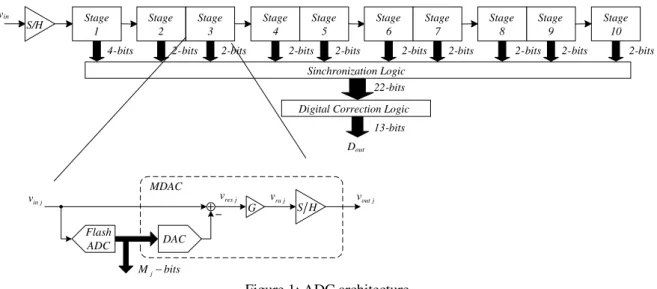
The ADC employs the pipeline architecture; this architecture allows obtaining a high speed and high resolution ADC. The Architecture is shown next in Fig. 1. This architecture employs 10 stages preceded by a sample and hold-circuit. Each stage is constituted by an MDAC circuit comprising a 4-bit (or 2-bit) flash quantizer, a sample and hold, gain and 4-bit (or 2-bit) digital to analogue converter. These functions are implemented by comparators and by a switched capacitor circuit. Stage 1 S/H Stage 4 4-bits 2-bits vin Sinchronization Logic 22-bits Digital Correction Logic
13-bits 2-bits Stage 2 2-bits Stage 3 Dout 2-bits Stage 5 Stage 6 2-bits Stage 10 2-bits 2-bits Stage 7 Stage 8 2-bits 2-bits Stage 9 Stage 1 S/H Stage 4 4-bits 2-bits vin Sinchronization Logic 22-bits Digital Correction Logic
13-bits 2-bits Stage 2 2-bits Stage 3 Dout 2-bits Stage 5 Stage 6 2-bits Stage 10 2-bits 2-bits Stage 7 Stage 8 2-bits 2-bits Stage 9 Flash ADC DAC
G S H MDAC
j in
v vresj vraj voutj
bits Mj−
Figure 1: ADC architecture
performance specifications. This optimization takes into account the thermal noise, the power dissipation, the differential non-linearity (DNL) and the total ADC capacitance. The best architecture optimization resulted in an ADC with three different pipeline stages and four different amplifiers. The optimizer provides another important set of design outputs including: optimum values for the unit capacitances required in each stage; optimum values for the compensation capacitances required in each stage; biasing currents to be used in the amplifiers; GBW specification for the amplifiers.
ELECTRICAL DESIGN
The selected amplifier topology uses a folded-cascode input stage followed by a differential-pair second-stage. Enhanced cascode-compensation [1] is used instead of the conventional Miller compensation in order to improve the bandwidth. The amplifiers are optimized using a proprietary optimization tool. A key input to the system is a file containing all relevant process technology parameters which are specific to the chosen fabrication technology. The specifications for each amplifier are obtained during the architecture optimization. The amplifier optimization takes into account the following key opamp features: low frequency gain, product gain-bandwidth, output swing, slew-rate, settling time, excess noise factor and gate area. Furthermore, the optimization is performed considering 17 different design corners simultaneously. The comparators used in the flash quantizers are designed using Monte Carlo analysis in order to verify the value of the offset due to mismatch errors. The complete ADC is simulated in all the relevant corners in order to verify the design.
IONIZATION EFFECTS
When an electron hole pair is created in the oxide by an ionizing particle or photon, the electron will disappear faster than the hole because the mobility of the electron is much higher than the mobility of the hole. The holes will tend to accumulate over time close to the interface layer between the oxide and Silicon. This accumulation corresponds to a positive charge that builds up over time [2].
Effects in Transistor Gates
If this positive charge occurs in the gate of a NMOS transistor it will lower the value of the transistor threshold voltage and increases the leakage current of the transistor. If it occurs in a PMOS transistor it will increase the modulus of the value of the threshold voltage of the transistors, making it more difficult to turn ON the transistor. It should be noted, that the same TID value can result in different magnitudes of this effect. If the TID value is obtained over a short period of time, with a radiation with a large intensity, there will be almost no time for the holes to migrate from the oxide to the Silicon, resulting in a large build-up of charge in the transistor gate and therefore resulting in a large shift in the transistor threshold voltage. If the TID value is obtained over a long period of time, with a radiation with a small intensity, the holes have time to migrate from the oxide to the Silicon, resulting in a small build-up of charge in the transistor gate and therefore resulting in a small shift in the transistor threshold voltage. The magnitude of the threshold voltage variation depends on the oxide thickness. As the oxide thickness reduces, so does the amount of charge build-up that occurs for a given TID value. It is expected that for 130nm technologies and beyond, TID does not cause serious problems regarding threshold voltage (VT) variations.
Effects in the Field Oxide
RADIATION ROBUSTNESS BY DESIGN
The threshold voltage variation effect due to TID can be mitigated by designing the circuits to be robust to the variations in the threshold voltage (VT) of the transistors. In the case of the ADC design, this can be done at circuit level
and at architecture level. At circuit level, it is necessary to improve the tolerance of the circuits to VT variations. This is
particularly important in the ADC comparators and in the amplifiers. The circuits are naturally robust to VT variations
because they use current biasing techniques and as long as the value does not increase too much, the bias circuit automatically compensates for the variations. Whenever possible the electrical design uses low VDsat values in the
transistors in order to have an extra voltage margin to accommodate for VT variations, e.g. due to TID. The comparators
will be designed to have a low offset voltage, also to accommodate the VT variations. It should be noted that these
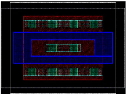
design strategies result in an increase in the power dissipation of the circuit and therefore it might not be possible to add a large safety margin to the design. At architecture level, the architecture of the ADC is naturally robust to offset variations in the comparators because it uses digital correction. The parasitic N channels that occur under the field oxide can be interrupted using P+ guard rings connected to ground. Ideally each transistor would be enclosed inside a guard ring, but this would result in a large area increase. Therefore, it is necessary to study with great care the placement of these guard rings during the layout of the ADC. These guard rings also improve the robustness of the circuit to SEE, because they provide a path for the carriers that are created by high energy particles, to dissipate quickly and increase the resistance in the parasitic NPNP structure making it harder for a latch up to occur. The parasitic N channels that appear on the edges of the NMOS transistor cause a leakage current to appear between the drain and the source of the transistor. This leakage current is not very important if the transistor is ON with a large drain current, such as the transistors in the op-amps. If the transistor is OFF and is inside a logic gate, the leakage current can draw a large current from the power supply, which can be a problem. If the transistor is a switch inside a switched-capacitor circuit, the leakage current can discharge the capacitors and cause signal attenuation in the system. The parasitic N channels that appear on the edges of the NMOS transistors can be eliminated if the transistors use enclosed layout (the source or drain of the transistor is enclosed by the gate). This solution is problematic because no accurate electrical models exist for this transistor structure. This structure is particularly adequate for transistors with large channel widths. It is expected that the electrical behaviour of a transistor with a large channel width, using this structure, is similar to the electrical behaviour of a regular transistor structure. The layout of an enclosed transistor is shown next in Fig. 2.
Figure 2: Layout of enclosed transistor.
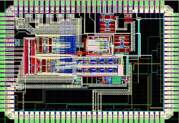
Figure 3: Layout of the test chip.
EXPERIMENTAL RESULTS
The performance of the ADC was measured using a dedicated test board with the silicon die placed directly on the board (circuit on board) in order to reduce the bond wire length and therefore its inductance value. Using this board the results shown in Table 1 were obtained for an input signal with 10 MHz frequency and amplitude 1 dB below full scale and a power supply voltage of 1.2 V:
Table 1: Key measured results.
Fs (MHz) SFDR (dB) THD (dB) SNR (dB) SINAD (dB) ENOB (bit) Power (mW)
40 76.00 -71.78 67.26 65.95 10.67 48.59
80 74.77 -72.77 64.84 64.22 10.38 92.41
The radiation tests of the ADC include TID characterization of the ADC and SEL test of the circuit. Three samples were irradiated with heavy ions with energies from 1 to 70MeV.cm².mg-1 to verify for SEL occurrences; the description of the ion mixture used in this test is shown next in Table 2. This test produced no observable SEL in the circuits.
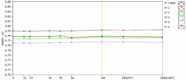
The measurement of TID effects in the performance parameters of the ADC (TID total dose of 100 krad(Si) was realized using 5 samples. Sample 1 was not irradiated and is used as reference. After the irradiation two annealing steps were performed: 24 h at 25 oC. and 168h at 100 oC. Thetest board and the circuit package used in the TID tests introduced a degradation in the measured ADC performance. This degradation is due to the long bondwires inside the package which have a large inductance. This causes the reference voltage values not to settle perfectly and thus the converted signal is corrupted by spurs. The measured SNR degrades if the sampling frequency is increased. Therefore the TID measurements of the ADC were performed with sampling frequency value of 40 MHz. Even using this lower sampling frequency, a degradation larger than 2 bits is observed in the ENOB value when comparing the measurements obtained using the board with circuit on board.
The measured voltage values of the positive reference voltage for different TID values are shown in Fig.4. This graph shows that the variation of the reference voltage with TID is lower than the variation of the voltage within the six samples.
Figure 4: Measured positive reference voltage value.
The measured SNR of the ADC as a function of the TID is shown next in Fig. 5, this graph shows that the SNR does not change significantly with the TID.
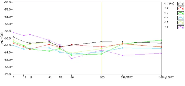
The variation of the THD as a function of the TID is shown next in Fig. 6, once again there are no significant variations with TID.
Figure 6: Measured THD.
The variation of the ENOB as a function of the TID is shown next in Fig. 6, once again there are no significant variations with TID.
Figure 7: Measured ENOB.
CONCLUSIONS
MHz. Three samples were irradiated with heavy ions with energies from 1 to 70MeV.cm².mg-1 and no SEL occurrences were observed. Five samples were irradiated up to a TID value of 100 krad(Si) and there was no significant performance degradation observed in the ADC.
Acknowledgements
The authors would like to thank the European Space Agency (ESA) for supporting this project and TRAD for performing the TID and SEL tests of the circuit.
REFERENCES
[1] Ahuja, B.K. “An improved frequency compensation technique for CMOS operational amplifiers”, IEEE Journal of
Solid-State Circuits, Dec 1983, Volume: 18, Issue: 6, pages: 629- 633