Edinei Santin
Engenheiro EletricistaA Built-In Self-Test Technique for High Speed
Analog-to-Digital Converters
Dissertação para obtenção do Grau de Doutor em Engenharia Electrotécnica e de Computadores
Orientador: João Carlos da Palma Goes, Professor Associado
com Agregação, Universidade Nova de Lisboa
Co-orientador: Luís A. Bica Gomes de Oliveira, Professor Auxiliar,
Universidade Nova de Lisboa
Júri:
Presidente: Prof. Doutor Paulo da Costa Luís da Fonseca Pinto Arguentes: Prof. Doutor Gildas Léger
Prof. Doutor Jorge Manuel dos Santos Ribeiro Fernandes
A Built-In Self-Test Technique for High Speed Analog-to-Digital Converters
Copyright c 2014 by Edinei Santin, Faculdade de Ciências e Tecnologia, and Universi-dade Nova de Lisboa
Acknowledgments
During my PhD journey I received direct and indirect contributions, support, advices from many generous persons, to whom I would like to express my indebtedness. Since my memory is not perfect and it fades over time (not as much different as real capacitors and inductors lose their states), I would also like to sincerely apologize those forgotten. For those lucky, I would like to particularly thank:
Professor João Goes, my supervisor, for his initial contacts, back in 2007, when I attended one semester of my undergraduate studies at Faculdade de Ciências e Tecnologia (FCT) of Universidade Nova de Lisboa (UNL). His strong commitment during that period was crucial for my decision of pursuing a PhD in his research group later.
Professors João Goes and Luís B. Oliveira, my co-supervisor, for all their support, patience, and collaboration. Under their supervision, I was always treated with consideration and respect. I hope that our friendship continues and that we may collaborate again in the future.
Professors Rui Tavares, Nuno Paulino, João P. Oliveira, and Adolfo Steiger Garção, all from the Electronics section of the Department of Electrical Engineering of FCT/UNL, for their collaboration and discussion about a diversified range of topics. Professor Rui Tavares was a close collaborator in several research papers, with his strong expertise in the optimization of analog circuits. Also, all laboratory users are in debt with him for all his dedication to keep the laboratory IT facilities (servers, CAD packages, licences, etc.) working properly almost uninterruptedly. Furthermore, he is a genuinely entertaining person, which make any interaction with him very enjoyable.
Professor Guiomar Evans, from Universidade de Lisboa, for collaboration in some research papers and for being a friendly person (with an admirable family).
Professor Antonio Petraglia and Fernando Barúqui, from Universidade Federal do Rio de Janeiro (UFRJ), Brazil, for the warm reception in their research grout at UFRJ for the two one-week meetings in the scope of a cooperation project, and for the pleasant stay at Rio de Janeiro. One scientific outcome of this collaboration was a journal paper.
Professor João Baptista dos Santos Martins, from Universidade Federal de Santa Maria (UFSM), Brazil, for accepting me in his Microelectronics research group at UFSM (right in the 2nd semester of my undergraduate studies!) and for being my supervisor and mentor until my graduation. Almost certainly, without that initial opportunity, I would have changed to another discipline other than Electron-ics/Microelectronis and, as a result, I would not be where I am now. Professor João Baptista was also who encouraged me to attend one semester of my undergraduate studies at FCT/UNL and, most importantly, introduced me to Professor João Goes (that was the “start” of this PhD).
My colleagues (labmates) Michael Figueiredo, José Rui Custódio, João Ferreira, Blazej Nowacki, Rui Borrego, Ivan Bastos, João de Melo, Somayeh Abdollahvand, Hugo Serra, Carlos Carvalho, and João Casaleiro. It was a pleasure to share the laboratory rooms with them, besides of the numerous discussions we had on distinct subjects. From lunch times to all-night-long preceding days to tapeouts, we lived the extremes of our journey. I had a closer collaboration with Michael Figueiredo, to whom I would like to double thank all the precious help he gave me, from useful CAD tips to several in-depth and productive discussions. Our collaboration eventually resulted in some interesting achievements that were recognized with some international awards.
My colleague Tiago Domingues for helping me in the layout of the preliminary version of the pipeline stages of the ADC. This help was essential to speed up the final layout of the ADC (one of the building blocks of the proposed system) and gave me more time for extraction simulations and correction of bad layout issues associated with that block.
Pedro Faria, Rui Monteiro, and Arnaldo Guerreiro, from S3 Group, for providing help to specific issues of the pipeline stages’ comparators and to the layout vs schematic verification of the Faraday’s input/output cells.
My Brazilian colleagues Marcelo Dal Alba, Tiago da Silveira, and Taimur Gibran Rabuske for their friendship, dinners together, and some travels to discover Portu-gal.
My Family, specially my mother Iracilde Bavaresco Santin, my bother Edgar Santin, and my grandparents João Santin and Teresa Durante, for all their support, encour-agement, and love. Even with the yearly-surmountable physical distance between us, they were able to transmit me peace of mind, even when my grandfather had to be hospitalized and, even with speaking limitations, wanted to speak with me on the phone to say he was recovering well and would be recovered within some days (and fortunately it was what happened).
The Centro de Tecnologias e Sistemas (CTS) of Instituto de Desenvolvimento de Novas Tecnologias (UNINOVA) for being my host institution. The CTS/UNINOVA staff, specially Magui Pereira, Paula Silva, Hugo Sousa, Mário Respeita, Francisco Ferro, and Rosa Rolo, were cooperative and diligent as much as possible.
The Faculdade de Ciências e Tecnologia (FCT) of Universidade Nova de Lisboa (UNL) for accepting me as a PhD student, and also for providing all the academic facilities (Library, Cantina, etc.) I needed.
And, finally, the Fundação para a Ciência e a Tecnologia (FCT) of Ministério da Educação e Ciência (MEC) for granting me a PhD grant (SFRH/BD/62568/2009) during four years of my PhD program.
Edinei Santin
Abstract
As the conversion rate trend of analog-to-digital converters (ADCs) keeps increasing, from the present state of few gigasamples per second range, their testing is becoming progressively more challenging, time-consuming, and costly. Aware to this fact, in this PhD work we investigate a novel solution to this problem. Specifically, we propose to use two small area oscillators inserted into two synchronized phase-locked loops (PLLs) to generate high frequency sinusoidal and clock signals and, on the digital side, to employ straightforward digital signal processing (DSP) techniques to dynamically and function-ally test high speed and moderate resolution ADCs. Using this built-in self-test (BIST) approach, the only off-chip component required is a low frequency and stable reference signal (e.g., produced by a ubiquitous crystal oscillator). The DSP techniques for output response analysis rely primarily on spectral computations, which nowadays are available in most system-on-a-chip environment through optimized fast Fourier transform algo-rithms; hence, reusing of the DSP resources is usually possible. The proposed concept was implemented in an integrated circuit featuring two PLLs for test stimuli generation and an 8-bit 500 MS/s ADC as the device under test, and was validated with silicon measurements. In a0.13µm CMOS technology, the area overhead introduced by the two PLLs is merely0.052 mm2.
Keywords: Analog-to-digital converter (ADC), built-in self-test (BIST), high speed
Resumo
Seguindo a tendência do ritmo de amostragem de conversores analógico/digital (ADCs), que atualmente já adentra sobre a faixa de bilhões de amostras por segundo, o teste des-tes dispositivos está progressivamente se tornando mais complexo, demorado e custoso. Cientes desta problemática, neste trabalho de doutoramento investigou-se uma solução para tal questão. Especificamente, é proposta a utilização de dois osciladores compactos, controlados por duas malhas de captura de fase (PLLs) síncronas, para gerar sinais de sinusoide e de relógio de alta frequência e, na parte digital, empregar técnicas de proces-samento digital de sinais (DSP) simples para testar ADCs de elevado ritmo de conversão e moderada resolução dinamicamente e funcionalmente. Empregando esta abordagem de auto-teste (BIST), somente um componente externo para gerar um sinal de referência de baixa frequência e estável (e.g., por meio de um oscilador a cristal) é necessário. As técnicas de DSP para análise da resposta de saída recaem principalmente na computação do espectro, muito utilizada atualmente em sistemas completamente integrado em silício através de algoritmos de transformada rápida de Fourier otimizados. Portanto, a reutili-zação de recursos de DSP é geralmente possível. O conceito proposto foi implementado num circuito integrado, contendo duas PLLs para geração dos estímulos de teste e um ADC de 8-bit e 500 MS/s como dispositivo sob teste, e foi validado com medições em silício. Numa tecnologia CMOS de0.13µm, o incremento de área introduzido pelas duas PLLs é de apenas 0.052 mm2.
Palavras-chave: Conversor analógico/digital (ADC), auto-teste (BIST), elevado
Contents
Acknowledgments vii
Abstract xi
Resumo xiii
Contents xv
List of Figures xix
List of Tables xxiii
List of Abbreviations and Symbols xxv
1 Introduction 1
1.1 Motivation . . . 1
1.2 Overview and Contribution . . . 2
1.3 Chapters Organization . . . 3
2 Basic Concepts 5 2.1 Analog-to-Digital Conversion Principle . . . 5
2.2 Static ADC Performance Metrics and Corresponding Testing . . . 7
2.2.1 Gain and Offset . . . 8
2.2.2 Differential Nonlinearity . . . 8
2.2.3 Integral Nonlinearity . . . 9
2.3 Dynamic ADC Performance Metrics and Corresponding Testing . . . 9
2.3.1 Discrete Fourier Transform and Coherent Sampling . . . 10
2.3.2 Signal-to-Noise and Distortion Ratio . . . 14
2.3.3 Total Harmonic Distortion . . . 17
2.3.4 Signal-to-Noise Ratio . . . 18
2.3.5 Spurious Free Dynamic Range . . . 18
2.3.6 Effective Number of Bits . . . 18
2.4 Role of Testing . . . 19
2.5 Characterization versus Production Testing. . . 21
3 Research Question 25
3.1 Problem Introduction . . . 25
3.2 Research Question . . . 27
3.3 Preliminary Observations. . . 27
4 Literature Review 29 4.1 Structural Built-In Self-Test for ADCs . . . 29
4.2 Functional Built-In Self-Test for ADCs . . . 33
4.2.1 Static Performance BIST Methods . . . 33
4.2.2 Dynamic Performance BIST Methods . . . 37
4.3 Discussion . . . 45
5 Proposed Approach 47 5.1 Generic ADC BIST Architecture . . . 47
5.2 Proposed ADC BIST Architecture . . . 48
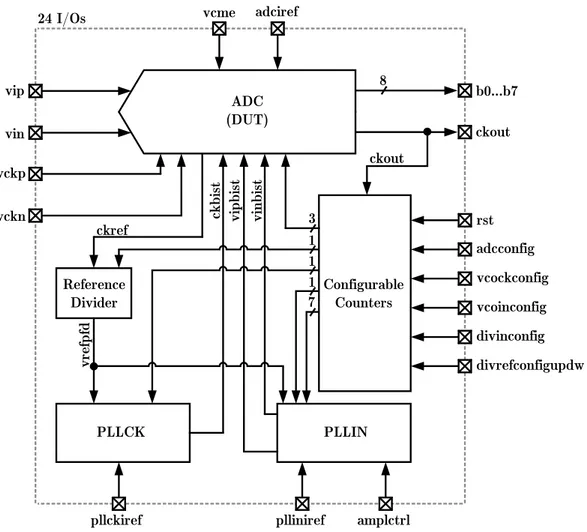
6 Prototype Implementation 51 6.1 Implemented System Overview . . . 51
6.2 BIST Circuitry: PLL IN, PLL CK, and Interfacing Circuits. . . 54
6.2.1 Analog Input Phase-Locked Loop (PLL IN) Overview . . . 54
6.2.2 Clock Phase-Locked Loop (PLL CK) Overview . . . 58
6.2.3 Voltage-Controlled Oscillators . . . 61
6.2.4 Phase/Frequency Detector . . . 73
6.2.5 Charge Pumps and Loop Filter . . . 74
6.2.6 Frequency Dividers . . . 77
6.2.7 Interfacing Circuits . . . 78
6.3 DUT Circuitry: High Speed Pipelined ADC . . . 83
6.3.1 Pipelined ADC Overview. . . 83
6.3.2 Interfacing Issues . . . 93
7 Experimental Results 97 7.1 Evaluation Board . . . 97
7.1.1 On-board Analog Input Interface Circuitry . . . 97
7.1.2 On-board Digital Input/Output Interface Circuitry . . . 99
7.1.3 Power Supplies and Biasing Circuitry . . . 100
7.1.4 Printed Circuit Board Layout . . . 104
7.2 Chip-on-Board Assembly . . . 106
7.2.1 I/O Pad Ring . . . 106
7.2.2 Chip-on-Board Process . . . 109
7.3 Test Setup . . . 109
7.4 Measurement Results . . . 113
7.4.1 DUT with External Analog Input and Clock . . . 113
7.4.2 DUT with External Analog Input and Internal Clock . . . 120
7.4.3 DUT with Internal Analog Input and Clock . . . 126
7.4.4 Complementary DUT Measurements . . . 129
8 Conclusions 137 8.1 Suggestions for Future Work . . . 138
A System Configuration 141
List of Figures
1.1 Overview of the proposed idea. . . 3
2.1 Ideal ADC model. . . 5
2.2 Ideal ADC transfer curve and quantization error. . . 6
2.3 Independently based DNL and INL definitions. . . 9
2.4 Two sine phase distributions depending on Np and Ns. . . 13
2.5 DFT processing gain. . . 14
2.6 Noncoherent spectrum versus windowed spectrum. . . 15
2.7 Windowed sequence. . . 15
2.8 Development cycle of an IC. . . 19
2.9 Setup for characterization and production testing. . . 22
4.1 DAC/ADC loopback BIST architecture. . . 30
4.2 Oscillation BIST architecture. . . 31
4.3 Structural BIST architecture for pipelined ADCs. . . 32
4.4 HABIST architecture. . . 34
4.5 Polynomial-fitting BIST architecture and low-pass filtered test stimulus.. 35
4.6 OBIST architecture applied to functional testing. . . 35
4.7 BIST architecture using low accuracy DACs for test stimulus generation. 36 4.8 Simplified MADBIST architecture for ADC testing. . . 38
4.9 Finite-length bitstream based test stimulus generator for BIST of ADCs. 40 4.10 Test stimulus generator based on ROM and DAC for ADC BIST. . . 41
4.11 FFT-based built-in self-test architecture. . . 42
4.12 DDS-based built-in self-test architecture. . . 43
4.13 Built-in self-test architecture with high frequency test stimulus generated by mixing. . . 45
5.1 Generic BIST architecture for an ADC. . . 47
5.2 Proposed BIST architecture for coherent testing of high speed ADCs. . . 48
6.1 Overview of the implemented system. . . 52
6.2 Top layout view of the implemented system. . . 53
6.3 Block diagram of the analog input PLL. . . 55
6.4 Layout of the analog input PLL and its floorplan. . . 57
6.5 Block diagram of the clock PLL.. . . 58
6.6 Layout of the clock PLL and its floorplan. . . 60
6.7 Block diagram of the two-integrator VCO and related circuits. . . 62
6.9 Schematic of the V/I converter and rail-to-rail buffer. . . 64
6.10 Detailed schematic of the rail-to-rail buffer. . . 65
6.11 Simulated discrete tuning characteristics of the two-integrator VCO. . . . 65
6.12 Simulated output THD of the two-integrator oscillator with and without the filtering capacitorCf. . . 66
6.13 Simulated start-up of the two-integrator oscillator showing the AAC re-sponse. . . 67
6.14 Simulated output amplitude of the two-integrator oscillator. . . 68
6.15 Schematic of the differential-to-single-ended converter employed in PLL IN. 69 6.16 Block diagram of the relaxation VCO and related circuits. . . 69
6.17 Schematic of the relaxation oscillator. . . 70
6.18 Simulated discrete tuning characteristics of the relaxation VCO. . . 71
6.19 Simulated phase noise of the relaxation VCO running in open loop and in closed loop. . . 71
6.20 Schematic of the differential-to-single-ended converter employed in PLL CK. 72 6.21 Simulated spectrum at the output of the DUT. . . 73
6.22 Zoom in of the relevant spectrum content of Fig. 6.21.. . . 73
6.23 Schematic of the phase/frequency detector employed either in PLL IN and PLL CK.. . . 74
6.24 Schematic of the charge pumps and third-order passive loop filter employed either in PLL IN and PLL CK. . . 75
6.25 Simulated up and down output currents of the main charge pump. . . 76
6.26 Schematic of the Ns frequency divider of PLL CK.. . . 77
6.27 Schematic of the Npi programable frequency divider of PLL IN. . . 78
6.28 Comparison between the super source follower and its modified version. . 80
6.29 Simulated THD of the linear buffer that drives the THA. . . 81
6.30 Schematic of the pseudo-differential linear buffer that drives the ADC input. 82 6.31 Simplified schematic of the configurable counters. . . 84
6.32 Block diagram of the 8-bit two-channel time-interleaved pipelined ADC. . 85
6.33 Layout of the 8-bit two-channel time-interleaved pipelined ADC. . . 91
6.34 Floorplan of the 8-bit two-channel time-interleaved pipelined ADC. . . . 92
6.35 Simplified schematic of the track-and-hold amplifier. . . 94
6.36 Simplified schematic of the on-chip clock circuitry. . . 95
7.1 Test board schematic: input/output analog and digital signals circuitry. . 102
7.2 Test board schematic: power supplies and biasing circuitry. . . 103
7.3 Test board layout. . . 105
7.4 Pads distribution around the I/O ring. . . 107
7.5 Photograph of a wire bonded die before glob top encapsulation and of a completely assembled test board. . . 111
7.6 Test setup.. . . 112
7.7 Photograph of the actual test setup.. . . 112
7.8 Measured SINAD, SNR, THD, and TI spur versusfs atfin≈10MHz and Vin≈ −0.1dBFS for three different samples. . . 116
7.10 Measured SINAD, SNR, THD, and TI spur versus fin at fs = 500 MS/s and Vin≈ −0.1 dBFS for three different samples. . . 118
7.11 Measured ENOB versus fin at fs = 500 MS/s and Vin ≈ −0.1 dBFS for
three different samples. . . 119
7.12 Measured output spectrum of Sample 1 at fs = 464.64 MS/s, fin =
56.265 MHz and Vin≈ −0.1 dBFS. . . 121
7.13 Measured SINAD, SNR, THD, TI spur, and ENOB versus fin at fs = 464.64MS/s and Vin≈ −0.1 dBFS for Sample 1.. . . 123
7.14 Measured SINAD, SNR, THD, TI spur, and ENOB versus fin at fs = 464.64MS/s and Vin≈ −0.1 dBFS for Sample 2.. . . 124
7.15 Measured SINAD, SNR, THD, TI spur, and ENOB versus fin at fs = 464.64MS/s and Vin≈ −0.1 dBFS for Sample 3.. . . 125
7.16 Measured output spectra of Sample 1 atfs = 464.64MS/s,fin= 226.875MHz
and Vin≈ −2.5 dBFS for the three test scenarios. . . 128
7.17 Measured SINAD, SNR, THD, and TI spur versusVCM Eatfs= 500MS/s,
fin ≈10MHz and Vin ≈ −0.1 dBFS for three different samples.. . . 130
7.18 Measured ENOB versus VCM E at fs = 500 MS/s, fin ≈ 10 MHz and
Vin≈ −0.1dBFS for three different samples. . . 131
7.19 Measured locking range of PLL CK for the slowest discrete tuning curve. 133
List of Tables
3.1 Summary of advantages and disadvantages of BIST. . . 28
5.1 Programmable parameters and frequency map for a 6-bit ADC. . . 49
6.1 Comparison of fully integrated CMOS oscillators. . . 61
7.1 Bill of materials. . . 106
7.2 Description of the chip pads. . . 110
7.3 Summary of the key frequencies of the slowest locking range of PLL CK. 132
7.4 Summary of the key frequencies of the fastest locking range of PLL CK.. 132
7.5 Performance summary and comparison with prior works. . . 135
A.1 ADC decimation, analog input, and clock configuration. . . 143
A.2 VCO CK discrete tuning configuration. . . 144
A.3 VCO IN discrete tuning configuration. . . 144
A.4 DIV IN division value configuration. . . 145
List of Abbreviations and Symbols
Abbreviations
AAC Automatic Amplitude Control
ac Alternating Current
A/D Analog-to-Digital
ADC Analog-to-Digital Converter
AMUX Analog MUltipleXer
ATE Automated Test Equipment
BIST Built-In Self-Test
CAD Computer-Aided Design
CMOS Complementary Metal-Oxide-Semiconductor
CODEC COder-DECoder
CP Charge Pump
DAC Digital-to-Analog Converter
dc Direct Current
DDEM Deterministic Dynamic Element Matching
DDS Direct Digital Synthesis or Synthesizer
DfT Design for Testability
DFT Discrete Fourier Transform
DIB Device Interface Board
DIFF/SE DIFFerential-to-Single-Ended
DNL Differential NonLinearity
DSP Digital Signal Processing or Processor
DUT Device Under Test
ENIG Electroless Nickel Immersion Gold
ENOB Effective Number Of Bits
ESD ElectroStatic Discharge
FD Frequency Divider
FF Flip-Flop
FFT Fast Fourier Transform
FSR Full-Scale Range
GBC Global Biasing Circuit
HABIST Histogram-based Analog Built-In Self-Test
HBIST Hybrid Built-In Self-Test
IDFT Inverse Discrete Fourier Transform I2C Inter-Integrated Circuit
IMD InterModulation Distortion
INL Integral NonLinearity
I/O Input/Output
IP Intellectual Property
IQ In-phase and Quadrature-phase
LC Inductor-Capacitor
LF Loop Filter
LFSR Linear Feedback Shift Register
LSB Least Significant Bit
LVDS Low-Voltage Differential Signaling
MADBIST Mixed Analog-Digital Built-In Self-Test
MDAC Multiplying Digital-to-Analog Converter
MOM Metal-Oxide-Metal
MSB Most Significant Bit
MUX MUltipleXer
OBIST Oscillation Built-In Self-Test
ORA Output Response Analyzer
OTA Operational Transconductance Amplifier
PC Personal Computer
PCB Printed Circuit Board
PFD Phase/Frequency Detector
PG Processing Gain
PLL Phase-Locked Loop
ppm Parts Per Million
PVT Process, supply Voltage and Temperature
PWM Pulse Width Modulation
RAM Random-Access Memory
RC Resistor-Capacitor
RF Radio Frequency
rms Root-Mean-Square
ROM Read-Only Memory
rss Root-Sum-Square
RZ Return-to-Zero
SC Switched-Capacitor
SFDR Spurious Free Dynamic Range
SINAD SIgnal-to-Noise And Distortion ratio
SiP System-in-a-Package
SMA SubMiniature version A
SNR Signal-to-Noise Ratio
SoC System-on-a-Chip
SPICE Simulation Program with Integrated Circuit Emphasis
SSO Simultaneous Switching Output
STG Symmetrical Transmission Gate
TG Transmission Gate
THA Track-and-Hold Amplifier
THD Total Harmonic Distortion
TI Time-Interleaving
TSG Test Stimulus Generator
UMC United Microelectronics Corporation
VCO Voltage-Controlled Oscillator
VCR Voltage-Controlled Resistor
V/I Voltage-to-Current
3D Three-Dimensional
Symbols
f Signal frequency (f = 1/T) [cycles per second, Hz]
fs Sampling frequency (fs = 1/Ts)[samples per second, S/s]
G Static gain of an ADC
N Resolution of an ADC [bits, b]
Np Number of integer periods of a periodic continuous-time signal
Ns Number of collected samples at ADC output
Nseq Number of collected sequences, each one with length Ns
Q Ideal code bin width of an ADC [e.g. volts, V] T[k] kth code transition level of an ADC [e.g. volts, V]
T Signal period [seconds, s] Ts Sampling period [seconds, s]
Vos Static offset of an ADC [e.g. volts, V] x(t) Continuous-time signal at time instant t x[n] nth sample of a discrete-time signal
X[k] kth DFT spectral component
Xos[k] kth one-sided spectral component Xosm[k] Magnitude of Xos[k]
Xosmav[k] Averaged magnitude ofXos[k] Xosmrms[k] rms magnitude of Xos[k]
Xwin[k] kth windowed DFT spectral component
Chapter 1
Introduction
In this introductory chapter, we first discuss the motivations behind the research line pursued in this work in Sec. 1.1. Then, in Sec. 1.2, we give an overview of the proposed idea and state the main contributions. Finally, in Sec. 1.3, we present the organization of the chapters throughout this document.
1.1
Motivation
The evolution of the complementary metal-oxide-semiconductor (CMOS) technology has been uninterrupted, allowing more efficient implementations of conventional digital-domain functions, and favoring the migration of other-domain functions to the digital domain at each new technology node. This efficiency gain and the innate advantages of the digital circuits (e.g. flexibility, robustness against surrounding noise, “unlimited” accuracy, etc.) are the main reasons behind the “never-ending” CMOS technology downscaling.
Despite of the interesting characteristics of the digital domain for implementing a variety of functions, most signals found in nature (e.g. sound, temperature, electromag-netic fields, etc.) cannot be directly processed by digital means. Therefore, after being represented into analog electrical signals (voltages or currents), these signals need to be converted to and from the digital domain through analog-to-digital and digital-to-analog converters (ADCs and DACs), respectively. ADCs and DACs are the most fundamental mixed-signal components, since they make the interfaces between the analog and digital domains possible.
The ADC interface, similarly as the DAC one1, assumes different forms depending
on its specifications. For example, the ADC required to digitize the electrical signal representation of a human voice is completely distinct from the one required to digi-tize a high frequency modulated communication signal. Hence, there exist several ADC architectures and their design, fabrication, and test may vary considerably. The three key specifications of any ADC are the resolution, the conversion rate, and the dissipated power, which entail several trade-offs depending on the particular architecture chosen and the technology used.
For certain applications, commonly found in communication and measurement indus-tries, high conversion rate (above 100 MS/s) ADCs play a crucial role in attaining faster
data processing, transmission, and usage. With the advances of the CMOS technology and the development of novel design techniques, the conversion rates of CMOS ADCs are now well beyond the gigasamples per second (GS/s) range [1–3]. Although the conversion rates for these applications are the highest possible, they generally require only moderate ADC resolutions (usually below 12 bits) [4]. These high conversion rate and moderate resolution ADCs are the ones we are primarily concerned in this work.
To ensure that these ADCs meet the specifications, and hence are qualified to be used in the envisaged applications, they need to be tested after fabrication and occasionally during in-field operation. The production test costs of such components represent today a very significant fraction of their production cost [5, p. 42], and these costs are perhaps the fastest-growing portion of the total manufacturing cost [6, p. 19] [5, p. 43]. These high testing costs are mainly due to lengthy test applications by means of extremely expensive automated test equipments (ATEs), which are required to apply specific test stimuli to the devices under test (DUTs) and collect and analyze their responses in the fastest possible way.
Since the conversion rates are foreseen to keep increasing [7], interfacing the ADCs to the test instruments raises new problems due to parasitics, trace mismatches, and interferences of either the printed circuit board (PCB) and the instrument test probes. This scenario becomes even more challenging with the today’s trends of system-on-a-chip (SoC), system-in-a-package (SiP), and the still recent three-dimensional (3D) chips [8,9], where the accessability of the ADCs for testing purposes through external equipments is becoming more and more restricted. Currently, this accessability problem can only be alleviated when an ADC and a DAC coexist into the same system, where the two can be combined to implement a fully digital test [10]. If it is not the case, however, the testing of such an ADC is extremely challenging.
1.2
Overview and Contribution
It is clear from the preceding discussion that today’s testing of high speed and moderate resolution ADCs poses remarkable challenges in terms of cost (due to expensive equipment and lengthy test applications), reliability (due to DUT and ATE interfacing issues), and also feasibility (due to restriction of pins for accessing the DUT).
To cope with these challenges, in this work we explore the possibility of using a dedicated built-in self-test (BIST) approach for testing these high speed and moderate resolution ADCs, either embedded into complex systems or as standalone components. This BIST approach is based on two compact and easy-to-integrate oscillators that gen-erate high frequency test stimuli (either analog input and clock) to the DUT. Currently, CMOS oscillators are able to reach oscillation frequencies in excess of 300 GHz [11]; hence, they naturally fit to the purpose of high frequency signals generation. Instead of using free-running oscillators for generating the analog input and clock test stimuli, we propose to synchronize the two oscillators with the aid of two phase-locked loops. This synchronization improves the phase noise of the generated signals and, more importantly, allows coherent sampling.
other circuits (optional)
ADC (DUT)
chip
in
V
ck
V
out
D
010
DD
V
others (optional)
ADC (DUT)
chip
Digital ATE out D
010 DD
V
BIST
Mixed-signal ATE
(optional)
Conventional
Approach ApproachProposed
Fig. 1.1: Overview of the proposed idea.
execution time and complexity. Besides of that, and assuming spectral analysis is used to evaluate the raw output data, a coherent sampled signal translates directly to a coherent spectrum, which avoids undesirable artifacts like spectral leakage.
In the context of this work, we are primarily concerned about the ADCs’ dynamic and functional performances, since ultimately they are what most matter in the testing of high speed ADCs [12, p. 241].
This fully integrated in CMOS technology BIST approach, which reduces test costs by avoiding the need of expensive mixed-signal ATEs, improves reliability by avoiding interfacing critical signals between the DUT and ATE, and enhances feasibility by carry-ing out the test procedure completely on-chip, is the main contribution of this work [13]. The conceptual overview of the proposed approach is shown in Fig. 1.1.
Even thought the DUT used in this work is based on a pipelined ADC topology, as it will be addressed later, the approach can be applied to other converter topologies with minimal effort, since it “sees” the device under test as an almost ideal “black box”.
1.3
Chapters Organization
This dissertation is divided into eight chapters and one appendix. Following this intro-ductory chapter, Chapter 2 introduces the basic concepts used throughout this work, namely: the static and dynamic performance metrics for ADCs and the standard test procedures used to determine them; the purpose of testing an integrated circuit; and the main differences between characterization and production tests and between structural and functional test approaches.
structural and functional built-in self-test approaches, with emphasis on functional ones, which are further analyzed in terms of their applicability to static or dynamic performance testing. The chapter ends with a discussion of the reviewed solutions and identifies research gaps which are then considered within this work.
Chapter 5 presents the proposed built-in self-test architecture for high speed ADCs conceptually. It also indicates how the programmable parameters of the architecture could be selected based on the desired normalized analog input frequencies, desired clock frequencies, desired external reference frequency, and on the resolution of the ADC. Based on these parameters, a frequency map, which indicates all possible analog input and clock frequency combinations available to stimulate the device under test, is readily computed. Chapter 6contains the details of the proof-of-concept integrated circuit implementa-tion. Special emphasis is given to the built-in self-test circuitry implementation, which may be ported to another ADC topology with minimal efforts, since the proposed ap-proach considers the device under test as an almost ideal “black box” (except with regard to the interfacing input/output impedances). The device under test implementation, in this particular case a pipelined ADC, is also covered in this chapter.
Chapter 7 shows the silicon measurement results for distinct test scenarios, starting with the standalone ADC evaluation where the BIST circuitry is completely disabled. By means of on-chip configuration digital counters controlled by external push-button switches, other test modes are evaluated until the case where the BIST circuitry is fully operational. These results are compared and then confronted to those of other approaches available in the open literature. This chapter also discusses the implementation of the evaluation board and the test setup employed to make the measurements.
Chapter 8 summarizes the whole work and presents some suggestions for future re-search and development.
Chapter 2
Basic Concepts
In this chapter, the background concepts related to this work are presented. First, in Sec.2.1, the fundamental aspects of the A/D conversion are introduced since, throughout this work, we will deal with ADCs, in particular, with their testing. Secs. 2.2 and 2.3
discuss the most commonly used performance parameters for ADCs, classified into static and dynamic. Emphasis is given for dynamic parameters, since they are the most valuable in the context of high speed ADC testing. In Sec.2.4, we briefly present the main need for evaluating a device, which is then complemented by Sec.2.5, where two testing scenarios, characterization and production testing, depending on the device’s development phase, are contrasted. The chapter ends with Sec. 2.6, which discusses the differences between functional and structural testing approaches, and points out why functional testing still maintains its predominance nowadays.
2.1
Analog-to-Digital Conversion Principle
The function of an ADC is to convert a continuous-time and continuous-amplitude signal into a discrete sequence of digital words. It needs, therefore, to perform time discretization by means of a sampler (sampling operation) and amplitude discretization through a quantizer (quantization operation). The model for an ideal ADC is illustrated in Fig.2.1. In general, quantization and sampling are nominally uniform [14, p. 1].
The input-output transfer curve of an ideal ADC, under the assumption of uniform quantization, can be represented by a staircase function and fitted with a straight line
quantization
analog digital
output
Ts
ADC
sampling input
FSR
Vm
a
x
−
Q
Vm
a
x
Vm
in
+
Q
Vm
in
T
[
k
]
T
[
k
+
1] input
analog output
T[1]
0 1
k
2N
−1
T[2N
−1]
straight line
W[k]
digital
(a)
−Q/2
analog input
Vm
a
x
Vm
in
quantization error
+Q/2
(b)
Fig. 2.2: Ideal ADC transfer curve, having full-scale range FSR and (2N −1) transition
levels, which correspond to an N-bit quantization (a) and resulting quantization error (b).
as shown in Fig. 2.2a. The transfer curve maps the sampled input signal of the ADC (represented as a voltage, in this example) to a corresponding digital output (here, rep-resented with the unsigned coding scheme). The input signal can range from a minimum to a maximum value,Vmin andVmax, respectively, which is denoted as the input full-scale range (FSR) of the ADC. For aN-bit resolution ADC, the FSR is divided into2N equally
sized code bins with nominal width Q, hence
Q= FSR
2N =
Vmax−Vmin
2N (2.1)
By convention, the lowest code bin is numbered 0, the next is 1, and so on up to the highest code bin, numbered (2N − 1) [14, p. 2]. Code bins are delimited by (2N −1)
code transition levels represented by T[k]. The actual kth code bin width is W[k] = T[k+ 1]−T[k] for k = 1,2, . . . ,(2N −2). With this convention, therefore, the first and
analog input magnitude where half of the digital outputs are greater or equal to code k while the other half are below code k [14, p. 34].
Since ADCs do not have a one-to-one input-output mapping (i.e., several input volt-ages are mapped to the same digital output), an inherent error denominated by quan-tization error exists. Referring to Fig. 2.2a, this error represents the difference between the staircase function and the fitted straight line, and is plotted in Fig.2.2b. For specific input voltages (e.g., a ramp signal or a sine signal mixed with appropriate noise) the quantization error can be treated as a continuous random variable uniformly distributed between−Q/2and+Q/2. In this situation, it is easy to show that the root-mean-square (rms) value of the quantization error will be [15, pp. 83-85]
rms quantization error = √Q
12 (2.2)
Since the rms value of a full-scale input sine signal isFSR/(2√2), the maximum theoret-ical signal-to-noise and distortion ratio (SINAD) for an N-bit ADC is
SINADmax = 20 log10 FSR/(2
√
2) Q/√12
!
= 6.02N + 1.76 [dB] (2.3)
The analog-to-digital (A/D) conversion of an actual ADC has other errors in addition to the quantization error shown in Fig. 2.2b. These errors can be classified into static and dynamic depending on the time derivative of the input signal observed at consecutive sampling instants. If the observed time derivatives are small, it means that the input signal slowly varies in time and its effects on the A/D conversion will be equivalent to a constant signal. Static and dynamic errors can be evaluated through several metrics which are discussed in the next sections (Secs.2.2 and 2.3).
2.2
Static ADC Performance Metrics and
Correspond-ing TestCorrespond-ing
In this section, the most common ADC static metrics, i.e., offset, gain, differential and integral nonlinearities (DNL and INL), are discussed. We mention them briefly, since for high speed ADCs these parameters do not lead to useful conclusions about the devices’ performance. The only exception is the integral and differential nonlinearities derived by sine wave histograms, where the frequency of the sine signal can be practically increased to reveal some dynamic limitations of the ADC. In this case, we call dynamic DNL and INL to oppose to their static counterparts, and the frequency of the sine wave as well as the sampling frequency must be specified.
The static parameters inform how accurate are the code transition levels of the actual ADC transfer characteristic with regard to the ideal one (see Fig. 2.2a). Hence, the first procedure in deriving the static ADC metrics is to obtain all code transition levels T[k] for k = 1, . . . ,2N −1. For this purpose, there are basically three methods: the feedback
loop, the ramp histogram, and the sine wave histogram [14, pp. 34-42].
an alternative method to obtain the ADC transfer curve by averaging the output codes related to a set of input signal levels. This method is explained in [14, pp. 42, 43].
2.2.1
Gain and Offset
The static gainGand offsetVos of an ADC are defined as the quantities by which the code transition levelsT[k]are multiplied and then added, respectively, in order to minimize the errors ε[k]defined in Eq. (2.4). Note that the right side of Eq. (2.4) represents the ideal code transition levels, with T1 corresponding to the ideal transition T[1] (see Fig. 2.3). This definition of G and Vos leads to the minimum difference between the input and the output signals, after the latter is converted to input units.
G×T[k] +Vos+ε[k] =Q×(k−1) +T1 k = 1, . . . ,2N −1 (2.4)
Depending on howε[k]is minimized, there are two definitions for gain and offset: terminal based and independently based [14, pp. 44, 45]. Terminal-based gain and offset are the values ofGandVos in Eq. (2.4) that set the errorε[k]of the first and last code transition levels to zero , i.e., ε[1] =ε[2N −1] = 0. Hence, by measuring the code transition levels
T[1]and T[2N −1], the terminal-based gain and offset are straightforwardly obtained.
When GandVos in Eq. (2.4) are found by minimizing the mean squared value ofε[k], the resulting gain and offset are denominated independently based. Using linear least-squares estimation techniques, the static gain and offset become, respectively, [14, p. 45]
G=
Q 2N −1
2N−1
X
k=1
kT[k]−2(N−1) 2N−1
X
k=1 T[k]
2N −1
2N−1
X
k=1
T[k]2−
2N−1
X
k=1 T[k]
2 (2.5)
and
Vos =T1+Q 2(N−1)−1
− (2NG−1)
2N−1
X
k=1
T[k] (2.6)
Whichever of the two definitions is used, it must be clearly specified. The indepen-dently based approach is the most common in practice.
2.2.2
Differential Nonlinearity
The differential nonlinearity is defined as the difference between the real and ideal code bin widths,W[k]andQ, respectively, divided by the ideal code bin width, after correcting for static gain. Mathematically, this becomes
DNL[k] = W[k]−Q
Q k = 1, . . . ,2
N
−2 (2.7)
Note that code bin widths W[0] and W[2N −1] are undefined, hence the corresponding
real transfer
Vm
a
x
Vm
in
analog output
0 1
k
2N −1 digital
T
[1]
T1
T
[
k
+
1]
T
[
k
]
T
[2
N
−
1]
W[k]
Q
DNL[k]
INL[k]
input ideal transfer
function
function
Fig. 2.3: Independently based DNL and INL definitions.
the DNL, we name the DNL according to the gain derivation procedure (i.e., terminal or independently based). The graphical representation of the kth independently based DNL value is shown in Fig. 2.3.
When the DNL is stated in a single value, it represents the maximum absolute value
|DNL[k]|for allk. We say code k is a missing code whenDNL[k]≤ −0.9[14, pp. 47, 48].
2.2.3
Integral Nonlinearity
The integral nonlinearity is the difference between the ideal and actual code transition levels, normalized to the ideal code bin width, after correcting for static gain and offset. When expressed in units of least significant bits (LSBs), the INL becomes
INL[k] = ε[k]
Q k= 1, . . . ,2
N
−1 (2.8)
Similarly to the DNL, the INL may be terminal or independently based depending on the gain and offset estimation. Fig.2.3 shows thekth independently based INL value.
A single INL value represents the maximum value of |INL[k]| for all codesk.
2.3
Dynamic ADC Performance Metrics and
Corre-sponding Testing
Since the building blocks of any real ADC have finite bandwidths and can only process finite amplitude signals, generally swinging within a fraction of the supply rails (VDD and
VSS), the behavior of the ADC changes as either the amplitude or frequency of the input
other circuitry, there exist a high likelihood of interferences from these circuits, which also modify the ADC’s behavior. These changes are associated with intricate dynam-ical phenomena which pose limits on the performance of the ADCs and are quantified through several metrics discussed within this section. Given that most ADC performance parameters are derived from spectral analysis, we begin explaining the discrete Fourier transform (DFT) and a sampling technique called coherent sampling. For each metric, we discuss the most commonly used testing approaches.
2.3.1
Discrete Fourier Transform and Coherent Sampling
Suppose an ADC is digitizing an input signal x(t) with a sampling frequency fs. After
Ns ×Ts seconds, where Ns and Ts (= 1/fs) are the number of digitized samples and
sampling period, respectively, we have a sequence x[n] with Ns samples. This
time-domain sequence may be represented in the frequency-time-domain applying the DFT, which is defined as [16, p. 644]
X[k] =
Ns−1
X
n=0
x[n]e−j2πkn/Ns k = 0, . . . , N
s−1 (2.9)
If we want to recover the sequencex[n]from its spectrumX[k], we can apply the inverse DFT (IDFT) as follows [16, p. 644]
x[n] = 1 Ns
Ns−1
X
k=0
X[k]ej2πnk/Ns n = 0, . . . , N
s−1 (2.10)
Note that a normalization factor 1/Ns is used in Eq. (2.10). This means that each
spectral component X[k] in Eq. (2.9) is scaled up by a factor Ns. This conclusion is
easily confirmed if we calculate, for example, the direct current (dc) spectral component by means of Eq. (2.9), which is X[0] =x[0] +x[1] +· · ·+x[Ns−1], and compare it with
the actual dc component value, which is the time average ofx[n], i.e.,(x[0] +x[1] +· · ·+ x[Ns−1])/Ns.
The spectrum derived by Eq. (2.9) ranges from dc to fs(1−1/Ns) with increments
of fs/Ns, which is the frequency resolution of the DFT. Furthermore, the spectrum so
obtained is two-sided represented meaning that X[k] =X∗[N
s−k] fork = 1, . . . , Ns−1,
where the symbol ∗ means complex conjugation. If Ns is an even integer, the spectral
componentX[Ns/2]does not have complex conjugation. In this case, the two-sided
spec-trum may be converted to the one-sided one (i.e., ranging from dc tofs/2) by multiplying
the components X[k]by a factor of two for k = 1, . . . , Ns/2−1. Therefore, the one-sided
spectrum comprises a set of Ns/2 + 1 spectral components as follows
Xos[k] =
X[k] for k = 0
2×X[k] for 1≤k≤Ns/2−1
X[k] for k =Ns/2
(2.11)
The magnitude of the one-sided spectrum after appropriate normalization is
Xosm[k] = |Xos[k]| Ns
where|x|means the absolute value ofx. WhenNsis an odd integer, slightly modifications
are needed to make the two- to one-sided spectrum conversion, since now the component X[Ns/2]does not exist. In this work, otherwise explicitly stated, we assume even integer
Ns.
Even though the one-sided spectrum contains only half the spectral components of the two-sided spectrum, both representations have the same spectral power. Hence, they can be used interchangeably, although the one-sided spectrum is the most used.
If we collect Nseq sequencesx[n], each one with Ns samples, and apply the DFT over
each of these sequences, the resulting Nseq spectrums will be slightly different due to inherent random artifacts (e.g. random noise, random interferers, etc.) present either in x(t) or introduced during the A/D conversion. Hence, the results obtained through the spectrums will vary accordingly, limiting the measurements’ accuracy and repeatability. To reduce the spectral variance, the magnitudes of the spectrums can be averaged as follows [14, p. 52]
Xosmav[k] = 1 Nseq
Nseq
X
n=1
Xosmn[k] k= 0, . . . , Ns/2 (2.13)
where Xosmn[k] represents the kth one-sided spectrum magnitude related to the nth
se-quence. Eq. (2.13) is an ensemble average and represents the one-sided averaged magni-tude spectrum. By concentrating on a given spectral component Xosmn[k], as n ranges
from 1 to Nseq, the magnitudes fluctuate around a mean value with a certain stan-dard deviation. It can be shown that this stanstan-dard deviation is approximately p
Nseq times higher than that obtained observing the fluctuations over several realizations of Xosmav[k]1. Therefore, the spectral magnitudes given by Eq. (2.13) are more accurate
than those given by Eq. (2.12).
The spectral magnitudes of Eqs. (2.12) and (2.13) may be represented in rms values. For Eq. (2.12), for instance, this becomes
Xosmrms[k] =
Xosm[k] for k = 0
Xosm[k]/√2 for 1≤k ≤Ns/2−1
Xosm[k] for k =Ns/2
(2.14)
The average power of a real-value sequence x[n], with Ns samples, may be written in
terms of the rms spectrum as follows
1 Ns
Ns−1
X
n=0
x[n]2 =
Ns/2
X
k=0
Xosmrms[k]2 (2.15)
where the Parseval’s theorem [16, p. 707] is used.
Thus far, we have imposed no restrictions on the input signal x(t) being digitalized by the ADC and then processed by DFT. However, the spectrum computed by the DFT will be correct only if the signalx(t)can be frequency decomposed into integer multiples of the frequency resolution of the DFT, i.e., kfs/Ns for k = 0,1,2, . . . This means that,
when the DFT is applied, the spectral components of x[n] will lie exactly on the DFT bins, i.e., kfs/Ns for k = 0,1, . . . , Ns−1. When this condition is satisfied, we say that
signal x(t) is coherently sampled.
For the special case of a sine signalx(t) =Asin(2πfint), with frequencyfin (= 1/Tin), being sampled by a sample ratefs, coherent sampling is achieved with [17, p. 45] [18]
fin = Npfs Ns
(2.16)
where Np is an integer number. Eq. (2.16) can be rearranged as follows: NpTin =NsTs,
whereNp may be interpreted as the number of input periods sampled during the sampling
interval (NsTs).
The computation of the DFT, exactly as defined in Eq. (2.9), requires a high compu-tational cost, specifically,N2
s complex multiplications and Ns(Ns−1)complex additions.
In practice, however, there exist more efficient ways to compute the DFT, which are called fast Fourier transform (FFT) algorithms [16, chap. 9]. It can be shown that these algorithms reduce the implementation complexity of the DFT to Nslog2Ns complex
multiplications and Nslog2Ns complex additions, if Ns is a power of two [16, p. 729].
Therefore, it is advisable and wise to collect a power of two number of samples to allow an efficient DFT computation. In this work, unless differently stated, we assumeNs= 2p
with a positive integer value p.
Sampling the sine signal x(t), with fin defined as in Eq. (2.16), at instants t = nTs,
for n= 0,1, . . ., results
x[n] =Asin
2πNpn
Ns
(2.17)
If we consider Ns = 24 = 16 and Np = 6, for instance, and collect Ns samples, the sine
signal will assume discrete-phase values of 2π(6/16)n, n= 0,1, . . . , Ns−1. Distributing
these phases on a circle produces Fig. 2.4a, where the index n for each sample is shown. It is clear from Fig.2.4a that the sequence x[n]contains only 8distinct values, since half of the samples overlap. In other words, the collected samples are somehow redundant. This occurs because Np/Ns is not irreducible in this example, i.e., Np/Ns = 6/16 = 3/8.
Hence, the phases overlap after 8 samples, instead of Ns = 16. By considering Np any
odd integer, the ratio Np/Ns is irreducible sinceNs is a power of two. In general,Np and
Ns must be mutually prime. Fig.2.4b shows the phases distribution when Ns = 16 and
Np = 7. Clearly, the Ns collected samples have distinct values.
From the ADC testing perspective, we want the minimumNsthat contains all possible
ADC codes. Hence, Np/Ns must be irreducible to avoid collecting redundant samples
when the input signal is periodic. With this condition fulfilled and assuming an ideal ADC sampling a full-scale sinusoidal, the minimumNs in order to get at least one sample
from every ADC code is [13] [14, p. 30]
Ns > π2N ≈2N+2 (2.18)
(a) (b)
Fig. 2.4: Phases distribution of a sine signal with reducible (a) and irreducible Np/Ns
(b). Ns = 16 for both cases and the circle is divided inNs slices.
The number of samples, Ns, also influences the processing gain (PG) of the DFT,
which is defined as [15, p. 88]
PG = 10 log10
Ns
2
[dB] (2.19)
This gain defines how much the DFT noise floor is below the maximum signal-to-quan-tization noise ratio given by Eq. (2.3). As an example, Fig. 2.5 shows the one-sided magnitude spectrum obtained through Eq. (2.12) over Ns = 4096samples. The samples
are derived from a 10-bit ADC with a FSR of one, which is sampling a full-scale sine signal, i.e. x(t) = (FSR/2) sin(2πfint), with fs = 100MS/s. The frequencyfinis selected
by Eq. (2.16) withNp = 483andNsgiven by Eq. (2.18), thus ensuring coherent sampling.
(Note that the Nyquist criterion [16, p. 160] is not obeyed if Np ≥ Ns/2. In this case,
the ADC is undersampling the input signal, which is commonly denoted sub-sampling operation mode.)
If Eq. (2.16) is not satisfied, the ADC samples the input signal noncoherently. In this situation, the signal will not be concentrated on a single DFT bin; instead, it will be spread among several bins, which is commonly known as spectral leakage. Fig. 2.6a
superimposes the coherent spectrum of Fig. 2.5 with a noncoherent spectrum obtained choosing Np = 483.5. It is noticeable that the resulting spectrum is unsuitable for
practical use.
To minimize the undesirable effects produced by noncoherent sampling, we can apply a window over the digitized sequence x[n], and then compute the DFT. The purpose of any window is to progressively reduce the amplitude of the sequence x[n] from its intermediate to its extremes samples. This idea originates from the fact that the DFT, even processing a single sequence x[n] with Ns samples, implicitly assumes the sequence
xc[n], formed by a contiguous arrangement of an infinity number of sequences x[n], has
Fig. 2.5: Output spectrum (4096-point FFT) of 10-bit ADC with FSR = 1, fs =
100 MS/s, and input signal x(t) = 0.5×sin(2π×(483/4096)×108t). The FFT noise floor is ∼33 dB below the maximum theoretical SINAD for this converter, i.e. ∼62dB, due to processing gain.
The spectrum of a windowed sequence is derived as follows
Xwin[k] =
Ns−1
X
n=0
w[n]x[n]e−j2πkn/Ns k = 0, . . . , N
s−1 (2.20)
which is similar to Eq. (2.9), despite now the sequencex[n] is multiplied by the window w[n].
Regarding the window selection, there are several options depending on the desired characteristics (see, e.g., [19, p. 55]). Perhaps the most used for ADC testing are the Flat Top and the Hann windows, which are defined, respectively, by Eqs. (2.21) and (2.22)
w[n] = 1−1.93 cos
2πn Ns−1
+ 1.29 cos
4πn Ns−1
−0.388 cos
6πn Ns−1
+ 0.0322 cos
8πn Ns−1
n= 0, . . . , Ns−1 (2.21)
w[n] = 0.5
1−cos
2πn Ns−1
n = 0, . . . , Ns−1 (2.22)
The Flat Top window changes almost negligibly the amplitudes of the signal x(t), and since most measurements are based on spectrum magnitudes, this window is largely employed. However, the Flat Top window is not adequate for frequency discrimination, given that the energy of the components are spread over several DFT bins. In this par-ticular case, the Hann window is more appropriate. Besides these two windows, there are many others, e.g., Hamming, Blackman, Blackman-Harris, etc. The windowed spectrum shown in Fig. 2.6b uses a Flat Top window.
2.3.2
Signal-to-Noise and Distortion Ratio
(a) (b)
Fig. 2.6: Noncoherent (a) and windowed (Flat Top window) (b) spectrums both overlaid with the coherent spectrum.
Fig. 2.7: Original x[n] and windowed w[n]×x[n] sequences. The window attenuates the amplitudes of x[n] at its extreme samples.
the clock signal. For each amplitude and frequency of the sine wave, the signal-to-noise and distortion ratio (SINAD) is computed as the ratio of the rms value of the sine signal to the rms value of the total noise at the ADC output. Mathematically, this becomes
SINAD = 20 log10
rms signal rms total noise
[dB] (2.23)
The total noise is any deviation between the output of the ADC, converted to input units, and the input signal, except deviations caused by gain, phase, or dc level shifts. Therefore, the amplitude accuracy and dc offset of the sine signal do not affect the SINAD result. Nonetheless, random noise and distortion do affect it and, consequently, appropriate filtering may be required depending on the quality of the available sine wave generator. Also, the frequency stability of the generator is an important concern, and it should be able to generate a low phase noise signal.
be misleading. Concerning the sine distortion, in practice, the amplitude of the dominant harmonic component of the sine signal should be at least12dB (or approximately 2bits) below the amplitude of the dominant harmonic distortion of the ADC [14, pp. 69, 70]. A similar rule of thumb may be applied to the random noise corrupting the sine signal, i.e., 12 dB below the ADC rms quantization noise. For the frequency stability, a maximum limit may be found relating the time jitter standard deviation of the sine signal to its nominal period [14, pp. 68, 69].
The amplitude and frequency of the sine wave influence the SINAD, hence for each measurement their values must be clearly specified. The minimum amplitude that can be processed by the ADC is restricted by the ADC noise floor. As the amplitude of the sine signal increases, the SINAD also increases until the distortions become dominant. For greater magnitudes, the SINAD decreases sharply. The dependence on frequency is usually monotonic, with the SINAD decreasing as the frequency of the sine signal increases. The most informative SINAD value is obtained when either the frequency and amplitude of the sine signal are pushed close to the maximum allowed values, which rely on the ADC bandwidth and full-scale range.
There are, basically, two test methods used to derive the SINAD: one based on the frequency domain and other based on sine wave fitting. The frequency domain method uses the DFT to first derive the spectrum and then compute the rms values of the sine signal and the total noise. A coherent spectrum, when practically feasible, is preferable to a windowed spectrum, as explained in Sec.2.3.1. Considering a one-sided rms magnitude spectrum (see Eq. (2.14)), the rms value of the total noise is given by
rms total noise =
s X
fk6=0,fin
Xosmrms[fk]2 (2.24)
where fk =kfs/Ns, k = 0, . . . , Ns/2. In Eq. (2.24), we removed the dc and fundamental
frequency (fin) components, and the remaining rms spectral components are combined in a root-sum-square (rss) basis. The rms value of the sine signal is found as follows
rms signal =Xosmrms[fin] (2.25)
The SINAD is then obtained by substituting Eqs. (2.24) and (2.25) into Eq. (2.23). If the measurement requires more accuracy, then the averaged spectrum defined by Eq. (2.13) can be applied. When a windowed spectrum is used to measure the SINAD, special attention must be paid to select the appropriate spectral components that form the rms signal and total noise values, since the energy of the signals are not confined in single DFT bins. In this situation, and depending on the characteristics of the window employed, adjacent bins should be considered for the dc and sine signal related spectral components [15, pp. 332, 333].
value is given by
rms total noise =
v u u t 1
Ns Ns−1
X
n=0
(x[n]−x[n])ˆ 2 (2.26)
where x[n] is the digital output of the ADC and x[n]ˆ is its best fit sine wave. The sine wave rms value is simply the amplitude of the fitted sine divided by √2.
Two well-known approaches for sine wave fitting are the three- and four-parameters least-squares fitting. The former is used when the frequency of the sine is known a priori, but the offset, amplitude and phase are not. A discussion of both methods may be found in [14, pp. 28, 29].
2.3.3
Total Harmonic Distortion
Differently from the SINAD, the total harmonic distortion (THD) accounts only for the harmonic components present in the ADC total noise. The harmonic components are a result of ADC nonlinearity and intricate dynamic phenomena when it is digitizing a periodic signal.
When the ADC is digitizing a pure sine wave (see Sec. 2.3.2 for a discussion on the sine wave purity) with certain frequency and amplitude, the THD is computed as the ratio of the rms value of a specified set of harmonic components to the rms value of the sine wave. In decibels this becomes
THD = 20 log10
rms harmonics rms signal
[dB] (2.27)
The set of harmonics considered in the THD must be stated when providing a THD measurement, as well as the amplitude and frequency of the input sine wave. Otherwise explicitly stated, in this work we consider the 2nd to the 10th harmonics, similarly as
in [14, p. 52]. When a given harmonic component cannot be distinguished from the ADC noise floor, it can be ignored from the THD computation.
Depending on the ADC bandwidth and full-scale range, the most useful THD value is obtained when the input sine wave assumes the highest amplitude and frequency al-lowed. This setup usually leads to the worst THD, since normally it worsens as either the amplitude and frequency of the sine signal increase.
The computation of the rms value of the harmonic components with enough accuracy needs an unambiguous spectrum, which is readily achieved with a coherent spectrum. When a windowed spectrum is used instead, special care must be given to the THD measurement, as discussed in [14, pp. 53, 54]. Furthermore, an averaged spectrum should be used whenever practical.
Considering an one-sided rms and coherent spectrum, the rms value of the harmonics is given by
rms harmonics =
v u u t
10
X
l=2
Xosmrms[fhl]2 (2.28)
where fhl = lfin represents the frequency (folded or not) of the lth harmonic. The rms
2.3.4
Signal-to-Noise Ratio
To derive the SINAD the ratio of the rms values of the sine signal to the total noise is used. If we remove from the total noise the harmonic components used in the THD measurement, then the signal-to-noise ratio (SNR) results
SNR = 20 log10
rms signal
rms non-harmonic noise
[dB] (2.29)
The rms value of the total noise excluding the harmonics, i.e., the non-harmonic noise, is
rms non-harmonic noise =
s X
fk6=0,fin,fhl
Xosmrms[fk]2 (2.30)
where the frequenciesfhlare the same used in Eq. (2.28). The rms value of the sine signal
is given by Eq. (2.25).
2.3.5
Spurious Free Dynamic Range
For an ADC digitizing a pure sine signal, the spurious free dynamic range (SFDR) is defined as the ratio of the sine wave amplitude to the largest amplitude in the whole spectrum after removing the dc and the sine wave spectral components. Mathematically, and considering an one-sided magnitude spectrum (see Eq. (2.12)), the SFDR turns to be
SFDR = 20 log10
Xosm[fin] maxfk6=0,fin(Xosm[fk])
[dB] (2.31)
where fk =kfs/Ns, k = 0, . . . , Ns/2. The function maxfk6=0,fin(Xosm[fk])finds the max-imum spectral component in the spectrum disconsidering the dc and the fundamental frequencies.
As for the other dynamic parameters discussed so far, the SFDR also depends on the amplitude and frequency of the sine signal. Consequently, the chosen amplitude and frequency must be specified with any SFDR measurement.
2.3.6
Effective Number of Bits
The effective number of bits (ENOB) performance parameter compares how close a real ADC is of an ideal ADC in terms of total noise. For a pure sine wave of specified amplitude and frequency, the ENOB is defined as follows
ENOB =N −log2
rms total noise rms quantization error
(2.32)
where N is the resolution of the ADC in bits. In Eq. (2.32), the rms value of the total noise is given by Eq. (2.24) or (2.26), and the rms value of the quantization error is given by Eq. (2.2).
The ENOB may be related to the SINAD as follows [14, pp. 67, 68]
ENOB = log2(SINAD)−log2√1.5−log2
Xosm[fin] FSR/2
Time Determine requirements
Define specifications IC design
Test development IC fabrication
Characterization testing Design refinement Fabrication
2nd pass characterization testing
Release to mass production Production testing
Customer
Good ICs to customer
Fig. 2.8: Development cycle of an IC.
where the SINAD is given by Eq. (2.23) (after converting to linear scale), Xosm[fin]is the amplitude of the digitized sine wave, and FSR is the full-scale range of the ADC.
In this section, we presented the most common dynamic metrics for evaluating an ADC as well as the test methods used to derive them. This coverage is sufficient for the purposes of this work; however, more dynamic metrics do exist. A more complete treatment can be found in the IEEE standard 1241-2010 [14]. We have noted that most test methods rely on a spectrum derived through DFT and coherent sampling.
2.4
Role of Testing
To better understand the purpose of testing an integrated circuit (IC), for example, an ADC, we firstly need to comprehend the development and production cycle of such a device. This cycle is divided in several phases, which are defined according to the business model of the IC manufacturer. For instance, a manufacturer having a vertically integrated business may deploy a development cycle beginning with the requirements for a specific device and finalizing with the concerns of in-field application for it [20, pp. 2– 7]. Here, instead of this holistic approach, we consider a reduced version starting with costumer’s requirements and ending with good packaged devices shipped to the customer, as illustrated in Fig. 2.8.
operate and the reliability needed under several environmental conditions. Furthermore, other characteristics such as production volume, cost, price, etc. are also specified.
Before proceeding in the IC development flow, the requirements and specifications should be checked against their feasibility. To this end, requirements and specifications are audited, which is a form of avoiding an unrealizable specification to reach the design phase [5, p. 8].
With the specifications defined and audited, the IC design takes place. The most recurrent design methodologies for mixed-signal ICs are the top-down and bottom-up methodologies, with their own strengths and weaknesses [21,22]. In a top-down design, without going into many details, for example, the design starts with a high-level be-havioral modeling of the architecture. Bebe-havioral model simulations, although not as accurate as electrical simulations, are much faster and allow the designer to evaluate several design choices and ideas which were not feasible otherwise. In the next step, the functionality of model is mapped to electrical circuits, which are then sized to meet the specifications, and more accurate electrical simulations are performed. The electrical and behavioral results are verified for agreement. If there exist a high correlation, the circuits are then laid out; if not, the circuits are resized and simulated again. After the layout is done, electrical simulations verify the conformance of post-layout simulation results with circuit-level (in the absence of parasitics) results. If the results are in accordance, then the IC is sent to fabrication.
Note that throughout the design phase several verifications are executed when chang-ing from one abstraction level to the next (e.g. from model to electrical circuits to physical layout). These verifications permit to identify a design error early in the design cycle, thus avoiding waste of time and cost, and precluding as much as possible an erroneous design to reach the fabrication step.
Concurrently to the IC design, the test development occurs. This involves the defini-tion of all testability issues, the elaboradefini-tion of a test plan and the design of the hardware (e.g., PCB) and software required for testing.
The layout data allows to generate the photomasks used for IC fabrication. The fab-rication process entails a sequence of steps which involve, for example, epitaxial growth, photoresist deposition, patterning through the exposure of photomasks to ultraviolet light, etching, ion implantation, oxidation, metallization, etc. (see [23, pp. 87–104] for details).
Unfortunately, the fabrication is not a perfect process. Impurities and material im-perfections, malfunction equipments, and human errors are some caused of defective ICs. The main reason for testing is to detect these defects, which cause an out of specification, or bad, IC [5, p. 8]. The testing gives no answer about what exactly went wrong. This answer is obtained through diagnostic analysis (diagnosis). The defects can be group into catastrophic or non-catastrophic (or soft). In the former, which may be a short or open trace, for example, the IC is not functional at all. In the latter, the specifications may vary slightly from one IC to another, and this may be caused by extra parasitic capacitance on a specific trace, for instance.