Abstract — Embedded test within integrated systems allows to overcome some of the difficulties found when testing using only an external tester. The work presented herein addresses the high level generation of specific programmable processors for testing different blocks in integrated systems, taking advantage of existing programmable resources.
This paper proposes a methodology to develop the processor's architecture from high level descriptions, and presents results on the application of this procedure to generate embedded tests for an A/D converter integrated into a mixed-signal application system.
Index Terms—Embedded analogue test, SoC test, test processor.
I. INTRODUCTION
HE progress attained in successive generations of electronic integrated systems (IS), either system-on-chip (SoCs), system in package (SiP), multi chip modules (MCM), and other implementation technologies, has created a new range of innovative and affordable consumer products. Blocks such as digital and analogue I/O interfaces, complex communication sub-systems (including optical and radio-frequency circuits), power management, and multiple processors (including the respective software) are now being integrated in ever shrinking single substrates.
Significant work has been done in the digital SoC testing domain, but, so far, the test of analogue and mixed-signal (AMS) cores has not been addressed by the IEEE 1500 workgroup due to its complexity and specificities [1 - 3].
The use of embedded processors to perform in-situ test operations has already been proposed. These operations include self-testing, memory tests, and the entire test of a SoC [4 - 9]. Both dedicated hardware and software facilities can be provided in these processors, such as boundary-scan
The work presented herein has been partly supported by the Portuguese government, Agência de Inovação, and carried-out under the framework of projects ASSOCIATE (A503 - MEDEA+) and NanoTEST (2A702 - MEDEA+, phase 2).
F. X. Duarte and Gabriel A. Pinho are with Universidade do Porto, Faculdade de Engenharia, and INESC Porto, Campus FEUP, Rª Dr. Roberto Frias nº 378, 4200-465, Porto, Portugal (phone: +351225081327; fax: +351225081443; e-mail: {fduarte,Gabriel}@fe.up.pt).
J. C. Alves, J. Machado da Silva, and J. S. Matos are with Universidade do Porto, Faculdade de Engenharia, and INESC Porto, Campus FEUP, Rª Dr. Roberto Frias nº 378, 4200-465, Porto, Portugal (phone: +351225081400; fax: +351225081443; e-mail: {jca, jms, jsm}@fe.up.pt).
controllers, LFSR and MISR registers, and programs for local test vector compression and decompression. A test support processor placed near the DUT (device under test) allows overcoming the effects of transmission lines at very high frequencies by reducing the effective distance between ATE pin electronics and the DUT [10]. In [11] an embedded AMS test controller is proposed which makes use of the IEEE 1149.4 standard [14] and utilizes the embedded memory to support test operations.
The recent advances in FPGA devices have been enabling the increasing use of this technology in complex AMS systems. The ability to accommodate several different functionalities backed-up in low-cost off-chip memory systems, the capability to support hardware upgrades and the performance afforded by dedicated digital systems are proven arguments favouring this trend. This has been observed during the past few years in PCB-assembled systems that include more and more FPGA devices; next years will certainly assist to a further integration of FPGA blocks, processors, as well as, analogue and mixed-signal cores into a single package.
Such uncommitted implementation area for custom logic within an AMS system is a very attractive resource, from the system test point of view. With the support for dedicated test-specific signals and buses, the same physical implementation area can host a variety of different circuits, each one specially designed to carry-out test tasks for the other blocks in the system [12].
Having a programmable processor running a stored program dedicated to this task has several advantages, when compared to test-specific circuits with fixed functionality. First, a stored-program processor offers some degree of flexibility because the overall operation is dictated by a sequence of instructions (software) and changes still supported by the instruction set do not impose a new hardware design cycle. Second, a common processor core can be surrounded by specific peripheral blocks supported by high-level instructions, to satisfy tight time requisites that may be imposed by some test operations. Examples of such blocks are test stimuli generators, data pre-processing, signature compaction, and test infrastructure controller. Finally, the always constrained implementation space of a reconfigurable block can be conveniently traded-off among processing power, flexibility of programming and the amount of data to be transferred to external equipment (this impacts significantly the testing time).
However, generating several different specific processor architectures and test programmes is a time consuming and errorprone task, when done from scratch at the RTL level, for
A High Level Test Processor and
Test Program Generator
Francisco X. Duarte, José C. Alves, José Machado da Silva, Gabriel Pinho, and José S. Matos
T
each new system or test operation [7].
The work presented herein addresses the automatic generation of dedicated custom processor architectures for specific test operations, as well as the corresponding test programs. This facility can be seen as disposing of a highly flexible and optimised embedded tester, supplied as an intellectual property (IP) module and its software. The approach being proposed is based in the implementation of a test processor as an Application Specific Instruction-Set Processor (ASIP), whose set of conventional and dedicated instructions are automatically derived from a software specification of the test operation to be implemented.
The rest of the paper describes, in section II, the motivation and the basic functionalities being proposed for the test processor, and in section III the synthesis procedure to automate the generation of custom test processors. Section IV presents the first experiments of the application of this approach to an industrial AMS system, with particular emphasis on the test of an ADC integrated circuit. Finally, the main conclusions are highlighted in section V.
II. FUNCTIONALITIES OF A TEST PROCESSOR
The main operations to be performed by a generic tester (irrespective of the circuit under test) are:
- test pattern/stimuli generation - test infrastructure control
- configuration of test modes and propagation of test patterns and responses
- capture and evaluation of responses
Generation, transport, and capture of analogue signals are critical aspects in AMS test. On-chip stimuli generation and response evaluation are operations which can avoid the necessity for complex AMS testers, and may contribute to prevent performance degradation due to extra circuitry. If stimuli have to be generated externally, the test infrastructure has to be controlled accordingly.
Modular testing of embedded cores can simplify test access and application. Within modular testing an embedded core is isolated from surrounding logic using a wrapper, while a test access mechanism (TAM) provides test data delivery from I/O pins [2]. Besides partitioning provided by the test infrastructure, reconfigurable logic can also be explored to promote modularity. This allows creating modules within cores not provided with a test infrastructure or whose dimension would not recommend its inclusion. In the end, modularity facilitates the reuse of pre-computed tests for individual cores or SOC partitions.
Another aspect concerns time control and the synchronization of analogue and digital events. Time is a critical aspect in SoC testing, and can be reduced by performing parallel testing. Often, different frequencies are required for different cores and thus simultaneously driving different channels at different data rates is a highly desirable function. Even if tests are run under the control of the external tester, an embedded test processor may help increase the number of cores tested in parallel, at each proper clock frequencies.
Self-testing implemented with the aid of the test processor, offers the ability to apply and analyze test signals at-speed on chip. This, in general, provides greater accuracy and shorter test time.
Other non conventional test operations may also be carried-out in-circuit, taking advantage of the processing facilities provided by the processor.
To reduce testing time, a test operation comprising the capture of a number of samples from an analogue module may be interrupted whenever a totally unexpected sequence of response values is captured. Although this is expected to be an unusual situation, it can avoid subsequent and not necessary test operations.
Τs
Faulty samples
∆V
Fig. 1 — Pre-screening of faulty samples.
For the case the test stimuli is a sine wave, the test interrupt criterion may be based on the detection of N consecutive data samples, whose differences (∆V) among them are, for example
S I f f A V V V or V =0, ∆ ≥2×∆ max: ∆ max = ×2π ∆ (1)
where A is the test signal peak amplitude, fI the input
frequency, and fS the sampling frequency. This establishes a
pre-screening criterion based on the fact that, being the input signal a sinewave, the slope of N consecutive samples cannot be neither 0 nor higher than 2 times the maximum slope of the input sinusoid (Fig. 1). Detecting a sequence of samples presenting these characteristics is considered as a catastrophic fault has occurred, and thus it is not worth to capture the full specified sequence of samples, required, e.g., to compute a functional parameter.
Taking advantage of the reconfigurable block, all these operations can be reused, and even updated with more efficient algorithms, during all system’s life-time cycle, with no need for any hardware changes.
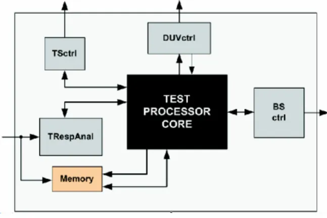
Figure 2 illustrates a simple block diagram of a possible test processor. It includes a programmable processor core surrounded with specific functional blocks, which may be included or not, depending on the type of test operations to be performed.
The base processor core supports a complete set of conventional instructions, plus high-level dedicated instructions that control the specific functional blocks placed around the core. The blocks diagram shown in figure 2 are:
− BSctrl is a boundary-scan controller implementing the IEEE 1149.1/4 standard protocol, used to control the existing test infrastructure
− TSctrl is a dedicated analogue stimulus generator comprising a DDS (Direct Digital Synthesiser) and a digital to analogue converter (a first-order Σ∆ modulator) − DUVctrl is a module responsible for controlling the
operation of the CUT
− TrespAnal evaluates the validity of the samples being captured to early detect abnormal responses
The actual configuration of the test processor is determined by the type of instructions the test designer uses in the test program. The processor’s instruction set is configured automatically from the source code of the program to be run, in order to include only the exact instructions required for that task. For example, if the processor's registers and the ALU operations are not referred in the program to be executed, these elements do not need to be included in the processor's datapath and control path; also, if a sinewave is needed as a stimulus, a special instruction must be used that will attach to the processor core the block to handle this function (the TSctrl block in the diagram of figure 2)
Although this strategy creates programmable processors that do not exhibit a high degree of flexibility because they just include the resources that meet the needs of one particular program, it is an efficient way to create dedicated controllers optimized in area for each particular test task. Besides, any test programs that use the same set of instructions can still be implemented without requiring the synthesis of a different processor.
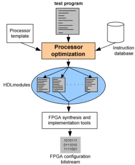
III. AUTOMATIC GENERATION OF SPECIFIC TEST PROCESSORS The generation of a test processor starts with a software specification of the test operation to be performed (figure 3). Presently, this specification is done using an assembly level language whose instruction set comprises all the core instructions supported by the processor, plus an extra set of complex instructions that are responsible for the operation of the peripheral specific blocks. From this specification, a custom programmable processor is generated as a set of synthesisable HDL modules, including the identification of peripheral blocks associated to specific instructions, and the set of constrains and assignments required to instantiate and
Fig.3 – Fluxogram of the test processor generation process. map these modules onto the FPGA. These descriptions are then forwarded to the specific FPGA technology mapping and implementation tools (the Foundation suite), to create an application-specific processor that includes only the instructions referred in the source code. The program to be downloaded onto the program memory is another output from the processor optimization process.
For example, the complex instruction TSTIMULUS generates an analogue test stimulus whose configuration (waveform, sampling frequency and amplitude) is specified by its operands. If this instruction is used in the test programme, the stimulus generation block (TSctrl in figure 2) is attached to the processor core, with the corresponding decoding and processing control states.
In a similar way, the basic processing and control flow instructions supported by the core processor are also included or not, depending whether they are referrenced or not in the source programme. This involves the customization of the processor’s control unit and datapath: type of operations implemented in the arithmetic and logic unit, number of general purpose registers and memory addressing modes.
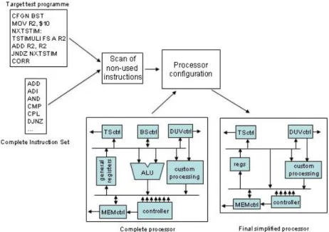
Instead of growing up the processor with the appropriate hardware support for the required instructions, the configuration process works, actually, in the oposite direction (figure 4). The starting point is a digital model of the full processor that supports the complete instruction set. By performing a single scan of the test programme, a list of the non-used instructions (either basic and complex), ALU operations, registers and memory addressing modes is constructed.
These unnecessary resources are then removed from the processor’s model in two phases. First, the datapath is simplified by deleting all the blocks that will not be used by that particular instance of the test programme. Then, the control path is optimised by eliminating all the states responsible for the control of the non-used instructions and adjusting the size and encoding of the control states.
Figure 4 – Configuration of test-specific programmable processors. The user can, if necessary, generate new instructions and/or
peripheral blocks. This process starts with the specification of the new instruction’s opcode and attributes (e.g. no. of operands and clock cycles), and with the identification of the interface with the core processor. This is carried-out using Perl data structures, one to describe the new instruction and another to describe the new block. The following Perl script shows the description of the DUVctrl block.
# Core interfacing signals //ctrlunit_interface eofduvtest, enduvtest, //ctrlunit_interface_end # output port //ctrlunit_output_port output enduvtest; reg enduvtest; //ctrlunit_output_port_end # input port //ctrlunit_input_port
input eofduvtest; //DUVctrl inport //ctrlunit_input_port_end # New core required logic //ctrlunit_input_event
eofduvtest or //ctrlunit_input_event_end # Initialization of type reg signals //ctrlunit_output_init
enduvtest = 0; //ctrlunit_output_init_end
# Inter-operability with the TEST_DUV instruction //ctrlunit_testop 4'b0011: begin enduvtest = 1; if ( eofduvtest ) nextstate = INITIAL; else nextstate = DECODE; end //ctrlunit_testop_end # External interfacing signals //mc_interface sclk, lrck, mclk, sinput, //mc_interface_end //mc_output_port output mclk; //mc_output_port_end //mc_input_port input sinput, sclk, lrck; //mc_input_port_end
# Instantiation of the block within the processor //mc_surround_blocks
wire enladseg_duv, rstladseg_duv, enradseg_duv, rstradseg_duv, eofduvtest, enduvtest;
wire [7:0] duvdata;
assign mclk = enduvtest ? clock : 0;
DUVctrl_cs5330A duvcrtl( .outsample(duvdata), .eofs2p(eofduvtest), .mem_we(mem_we_duv),
.enladseg(enladseg_duv), .enradseg(enradseg_duv), .en_dataaddr(endsaddr_duv), .sels2p(selS2P), .mclk(clock), .sclk(sclk), .lrck(lrck), .reset(reset), .ens2p(enduvtest), .sdata(sinput), .endds(endds) ); //mc_surround_blocks_end
# Interfacing with the core processor //mc_core_interface
.eofduvtest(eofduvtest), .enduvtest(enduvtest), //mc_core_interface_end
I. EXPERIMENTAL RESULTS
Fig. 5 – Diagram of the prototype system under evaluation. Figure 5 illustrates the prototype system being used as a validation vehicle. This is the front-end conditioning circuit of
the signals acquired from the voltage and current sensors of a digital energy meter. The test scheme being proposed here aims to provide an on-system self-test procedure to verify the functionality of the ADC and the analogue front-end circuitry.
This system includes a two-input sigma-delta ADC, and two input filtering and impedance adapter circuits. The ADC interfaces with the systems’s FPGA through 3 clock and one serial data digital signals. A memory block already existing in the system (not shown) and used by the application is also connected to the FPGA and is used by the test processor to store the responses acquired during the test operation.
An IEEE 1149.4 test bus [13] is used to gain access to selected analogue test nodes. The test bus is implemented by two 1149.4 compliant chips (SCANSTA400), which are controlled by a dedicated control block placed in the FPGA. These interface chips were inserted between the two primary analogue inputs and at the two ADC inputs, to provide analogue controllability at these nodes. These cells allow to select between mission signals and test stimuli generated by the stimuli generator included into the FPGA.
In this system the ADC digital interface signals are directly connected to the FPGA, and thus it is not actually necessary to switch them between mission and test modes, as both functionalities are controlled from the FPGA. Would this not be the case, specific digital wrapper cells would have to be inserted to switch between normal operation (mission signals) and the test specific stimuli. The analogue test cells implemented with the STA400 chips were inserted to allow performing the test of two signal paths per channel, i. e.:
- each ADC channel individually
- the input adapter and the ADC in a single path
Performing first the test of the ADC one can check its functionality before testing also the input adapters. The test can be stopped after each one of these operations if faults are found, to reduce total testing time.
The maximum allowable measurement error of the energy meter is 2%. This requires the maximum allowable measurement error per channel to be at most 1%. The performance of the test setup affects itself directly the test accuracy results. The final error measurement is determined by different error sources, such as:
- stimulus harmonic distortion - stimulus amplitude and phase noise - CUT’s harmonic distortion
- number of samples acquired to calculate the parameters - gain and offset deviations
- clock jitter
The overall contribution of these error sources determines the test tolerance band, and thus should not be higher than the maximum admissible error per channel. If the error sources are not correlated the total error becomes:
2 2 2 2 1 max ε ε ... εE ε = + + + (2)
where E is the number of errors being considered. In our case
E can be reduced to 4, because of:
- stimulus and CUT’s harmonic distortion can be joined together as a single harmonic distortion source
- stimulus phase noise is more critical than clock jitter - the CUT ADC included presents a high-pass behaviour
which eliminates analogue offset
- in the measuring process the noisy lowest significant bits can be omitted, and correlation provides also random noise filtering.
Taking this into consideration, the only error sources to be considered are stimulus phase noise, harmonic distortion, gain error, and the number of samples. Assuming equal contributions for the four sources, each one should be made lower than -52 dB from the fundamental signal amplitude, per channel. Concerning only harmonic distortion, and considering that this is due mainly to the first 4 harmonics, in the worst case – i.e., all have the same amplitude – each one of these should not be higher that -64dB. As an ADC with very low THD is used, the harmonic distortion required for the test stimulus can be determined by the maximum allowed error rather than by the CUT itself, and this allows to alleviate the test circuitry performance requirements.
A prototype of the test processor was implemented to support the test of this circuit, based on the computation of the cross-correlation between the circuit responses and the stimuli applied, to estimate the amplitude if the harmonics and derive the total harmonic distorsion (THD).
The circuit was synthesised for the system’s FPGA (XC4013E-4 PG223 [15]), occupying 85% of the CLBs and meeting the 8MHz target clock frequency. This implementation runs a very simple programme that configures the analogue bus through the JTAG interface to apply the analogue stimulus to the ADC inputs, activates the sine wave generator and captures a set of 16384 samples at a sampling frequency of 25.6KHz, storing them into the system’s memory.
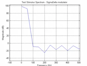
Fig. 6 – Stimulus’s spectrum at the Σ∆ output.
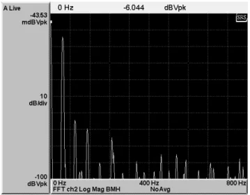
bit samples at a sampling frequency of 25.6KHz. Figure 6 illustrates the stimulus’s distortion obtained from the logic values captured at the sigma-delta output. It can be seen that the first four harmonics of interest present amplitudes below -88dBc.
The spectrum measured after the external filter (figure 7) shows a low-frequency distortion which do not satisfies the condition stated above to guarantee the 2% maximum error in the energy measurement (each one of the first 4 harmonics below -64dB). This distortion was found to be due to interference from the mains supply and could be removed even with low cut-off frequency filters.
The results obtained performing on-chip cross-correlation confirm the this spectrum, giving average values of -52 dBc for the 2nd harmonic, -58dBc for the 3rd harmonic, and -73dBc for the 4th one.
Fig. 7 – Stimulus’s spectrum at the filter output.
The cross-correlation is evaluated by a dedicated module associated to the core processor that processes data samples on the fly and that do not requires additional memory to store the captured samples.
V CONCLUSIONS
This paper proposes a design methodology to build application specific programmable processors to support the test of analogue and mixed signal blocks. Such test processor reuses a FPGA-like block that is now being a common place in AMS system boards, and will sonner or later move into more integrated tecnologies like SiP and SoC. A fully automated procedure is being implemented that generates synthesisable HDL models of a highly customised test processor, starting from a test programme specification.
The test of the analogue front-end of a digital power meter being used as test vehicle was presented. The necessity to
optimize the tests to be performed for area, power consumption and time duration, lead to different optimization goals that are being considered during the test generation.
ACKNOWLEDGMENT
Authors are thankful to TECMIC for valuable support.
REFERENCES
[1] E. J. Marinissen, R. Kapur, M. Lousberg, T. McLaurin, M. Ricchetti, Y. Zorian, “On IEEE P1500’s Standard for Embedded Core Test”, Journal of Electronic Testing – Theory and
Applications, Vol. 18, No. 4/5, Aug./Oct. 2002.
[2] IEEE P1500 Web Site, http://grouper.ieee.org/groups/1500 [3] A. Sehgal, S. Ozev, and K. Chakrabarty, “TAM optimization for
Mixed-Signal SOCs using Analogue Test Wrappers”,
Proceedings of the IEEE International Conference on Computer Aided Design, San Jose, November, 2003.
[4] C. Galke, M. Pflanz, and H. T. Vierhaus, “A Test Processor Concept for Systems-on-a-Chip”, Proceedings of the IEEE
International Conference on Computer Design: VLSI in Computers and Processors (ICCD’02), Germany, September 2002.
[5] Abhijit Jas and Nur A. Touba, “Deterministic Test Vector Compression/Decompression for Systems-on-a-Chip Using an Embedded Processor”, Journal of Electronic Testing – Theory
and Applications, Special Issue on SOC (System-on-a-chip) Testing for Plug and Play Test Automation, Vol. 18, No. 4/5, August/October 2002.
[6] Lai, W. -C. and Cheng, K. T., “Instruction-Level DFT for Testing Processor and IP Cores in System-on-a-Chip,” Proceedings of the 37th Design Automation Conference, pp. 58-64, 2001.
[7] O. Goloubeva, M. Sonza Reorda, M. Violante, "High-level test generation for hardware testing and software validation",
HLDVT2003: IEEE International Workshop on High Level Design Validation and Test, pp- 143-148, 2003.
[8] F. Corno, M. Sonza Reorda, G. Squillero, M. Violante, “On the Test of Microprocessor IP Cores”, Proceedings of the IEEE
Design Automation and Test in Europe Conference, pp. 209-213, 2001.
[9] R. Rajsuman, “Testing a System-on-a-Chip with Embedded Microprocessor”, in Proceedings of the International Test
Conference, pp. 499-508, 1999.
[10] D.C. Keezer, Q. Zhou, “Test Support Processors for Enhanced Testability of High Performance Circuits”, Proceedings of the International Test Conference, pp. 801-809, October 1999. [11] M. AbdEl-Halim, “An Analogue Mixed-Signal Test
Controller”, Proceedings of the IEEE Midwest Symposium on
Circuits and Systems, Oklahoma, 2002.
[12] M. Abramovici, C. Stroud, M. Emmert, “Using Embedded FPGAs for SoC Yield Improvement”, Proceedings of the Design Automation Conference, June 2002.
[13] IEEE 1149.4 - Standard for a mixed-signal test bus, Test Technology Technical Committee of the IEEE Computer Society, June 1999.
[14] SCANSTA400 – IEEE 1149.4 Analogue Test Access Device, National Semiconductor.