288
DC ANALYSIS OF p-n-p-n TUNNELING FIELD-EFFECT TRANSISTOR
BASED ON In
0.35Ga
0.65As
B. DOROSTKAR*, S. MARJANI**
Electrical Engineering Department, Iran University of Science and Technology, Tehran, Iran Department of Electrical Engineering, Ferdowsi University of Mashhad, Mashhad, Iran
behnamdorostkar@gmail.com*, saeid.marjani@mail.um.ac.ir** Received 31/07/2017 – Accepted 06/02/2018 DOI: 10.15628/holos.2018.6173 ABSTRACT
Using calibrated simulations, we report the In0.35Ga0.65As
based tunnel field-‐effect transistor (TFET) with thin δ-‐ doped n+ pocket at the source-‐channel interface to improve the parameters such as on current (Ion), off-‐
current (Ioff) and subthreshold swing (SS). The
simulations results of proposed device is compared with analytical model that is shown with high precision of DC parameters by examining the effects of III-‐V semiconductor materials. Furthermore, the influence of
pocket doping, pocket width, doping level, effective oxide thickness (EOT), temperature and mole fraction of III-‐V semiconductor material on device performance have been investigated. The results show that proposed device has a higher ON current (1×10-‐5 A/µm) and a
steeper subthreshold swing (35 mV/decade) as compared with the conventional TFET. It shows a lot of promise for future scale CMOS technology for low voltage and high frequency application.
1. INTRODUCTION
In the recent years, increasing utilization of portable device and wireless communication system caused ultralow power and high speed circuit to be interested under focus of which including SRAM, operational transconductance amplifiers (OTAs), analog to digital convertor(ADC) and current mode logic applications (marjani, et al., 2017; Bi, et al., 2017). It is clear that MOSFET is limited in subthreshold swing (SS) (60 mV/decade at room temperature) in recent technology (nanoscale system design) So tunnel field-‐effect transistor (TFET) is considered the best substitute for conventional CMOS (Zhao, et al., 2011). Enhance the current and steep subthreshold swing (below 60 mv/decade) are reliable trait as compared with MOS technology in ultralow voltage and high frequency applications (Vallett, et al., 2010; Ionescu and Riel, 2011). The method of carrier relocation is band-‐to-‐band tunneling (BTBT) (Zhu, et al., 2013) model which this phenomena betide between the source region and the channel region (Khayer and Lake, 2009). High ON current (Ion), low OFF current (Ioff) and steep subthreshold swing are
superior trait that make it distinguished from other devices. Also the biggest challenge is to design transistors that show simultaneously low threshold voltage and power consumption while maintaining reasonable current drivability. The silicon-‐based TFET exhibits a low sub-‐threshold swing and OFF current, but low ON current was controversial because of the low inter band tunneling (Guo, 2011). In order to achieve proper characteristics in terms of high Ion to Ioff ratio
and steep subthreshold swing, many structures have been suggested such as high-‐k dielectric materials (Boucart and Ionescu, 2007), pocket doping (Jhaveri, et al., 2011; Kao, et al., 2013; Chang, et al., 2013; Marjani and Hoseini, 2014a), double-‐gate (DG) TFET (Narang, et al., 2011), extended source (Marjani and Hoseini, 2015a), band gap engineering (Ganapath and Salahuddin, 2011) and multi gate structure (Marjani and Hoseini, 2015b). We can say several researchers have reported devices with SS below 60 mV/decade at room temperature in term of theoretically and experimentally (Brouzet, et al., 2015; Wu, et al., 2016; Marjani, et al., 2016b). The III-‐V compounds have much lower effective masses, higher electron and hole mobility when compared with the silicon. Many structures in term of homo-‐junction and hetrojunction are design by low band gap materials, such as Germanium, Silicon-‐Germanium and Gallium Antimonide (GaSb) can be employed for source region, whereas, Indium Phosphide (InP) can be used as a high band gap material for drain and channel region (Low, et al., 2016).
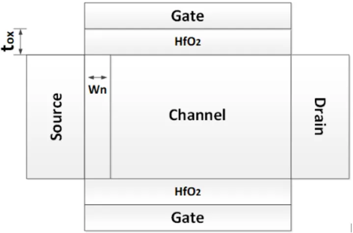
Figure 1: The schematic structure of double gate In0.35Ga0.65As p-‐n-‐p-‐n TFET.
In this paper, TFET with a δ-‐doped n+ region at the source side with III-‐V compound
semiconductors of InxGa1-‐xAs is proposed and evaluated. Also, the proposed structure is
optimized in term of pocket parameters. The rest of paper is organized as follows: In section 2, we describe the device proposed structure based on group III-‐V semiconductor materials and analytical model will be analysed. Section 3 show the DC analyses for the proposed TFET, the conclusions can be seen in section 4.
Figure 2: Simulated energy band diagram of proposed device in the off-‐state and the on-‐state
2. ANALYTICAL MODEL AND DEVICE STRUCTURE
The energy band diagram along the horizontal direction under the oxide-‐silicon interface is shown in Figure 2 for the off-‐state (VGS = 0 V and VDS = 1 V) and the on-‐state (VGS = VDS = 1 V) of
20 nm channel length In0.35Ga0.65As p-‐n-‐p-‐n TFET. Since the p and n regions are degenerately
Boltzmann's approximation cannot accurately describe carrier statistics in these regions.Therefore,expressions for potiontial barrier use the approximation of Fermi–Dirac distribution. In the channel region the expression for the electric field is (Gholizadeh and Hosseini. 2014):
( )
x 1 dx ε ρ ε =∫
1where ρ is the charge density. For p-‐n-‐p-‐n structre, the expression described as (Hosseini and Moghaddam, 2015; Marjani and Hoseini, 2015c):
( )
(
)
(
)
(
)
0 0 ( ) S P P S S P S S S P I S S S S P I D N S S S S qN X X X X qN X qN X X W x qN X qN W qN W X W X W L qN X qN W qN L qN X W L W L X W L X ε ε ε ε ε ε ε ε ε ε ε + + + ⎧ + − 〈 〈 ⎪ ⎪ ⎪ + 〈 〈 ⎪ ⎪ = ⎨ ⎪− + + − + 〈 〈 + ⎪ ⎪ ⎪− + − + − + + 〈 〈 + + ⎪ ⎩ 2Depletion region lengths in p and n regions are xp and xn, respectively. The band-‐to-‐band
tunneling rate and the tunneling current in junction region can be gained by (Marjani, et al., 2016a): 3 2 * * 2 2 2 0/5 . 2 2 r r BTBT g q m m Eg G E exp h E qhE π φ π ⎛ ⎞ − ⎜ ⎟ = ⎜ ⎟ Δ ⎜ ⎟ ⎝ ⎠ 3 In whichm* is the electron effective mass, Eg and
φ
Δ are the band gap and energy range in the tunneling region length, respectively E is total electric field at the tunneling junction.
* * *
1/mr =1/mh +1/me 4
where m is effective mass. The source drain tunnel current of pnpn TFET is given by (Hosseini and Moghaddam, 2015):
BT
DS G BTd
I =q
∫
v 5
where V is the three-‐dimensional device volume where tunnel paths start. We indicate that analyticaly drain current and the simulation based drain current closely match.
Figure 1 shows the cross sectional view of of proposed structure with channel length of 20 nm. The source and drain of conventional TFET structure are regions with high doped. The proposed structure is InxGa1-‐xAs based p-‐n-‐p-‐n TFET that the tunneling junction is formed
between the source and n-‐pocket that helps to reduce the tunneling width and thus improves the Ion and SS. One requirement to achieve optimum TFET performance is a low effective energy barrier for band-‐to-‐band tunneling and a small effective mass of the charge carrier. Therefore, structures based on all-‐III–V materials are very attractive because their effective bandgap can be engineered. The simulated device has a intristic channel doping concentrations of 5× 1015 cm-‐3 with a 20 nm channel length. The drain region is n+ with doping concentration of 2×1018 cm-‐3 and the source region with doping concentration of 2×1020 cm-‐3. This asymmetrical doping profile between the source and drain regions is commonly used for reducing ambipolar effects. Also, in order to improve the gate control, double gate structure is employed. The gate oxide thickness is 3nm and work function of the metal gate is 5.3 eV. The high-‐k dielectric materials (HfO2) is used
to improveing the Ion and hence achieve high on to off current ratio. the drain voltage is set 1 V for low voltage applications.
Figure 3: The energy band diagram of In0.35Ga0.65As p-‐n-‐p-‐n TFET with different Wn.
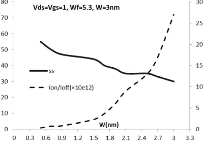
Figure 4: Ion/Ioff and SS of In0.35Ga0.65As p-‐n-‐p-‐n TFET as a function of Wn.
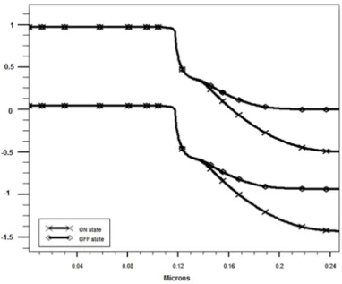
Figure 5: IDS-‐VGS of In0.35Ga0.65As p-‐n-‐p-‐n TFET with 20 nm of channel length and 3 nm of pocket width in simulation
3. RESULTS AND DISCUSSION
Silvaco TCAD software (Atlas, 2010) was adopted for the simulation of proposed structure. In this simulation tool, a uniform doping profile is used for all regions. Due to the unique characteristics of the TFETs some models have been used including nonlocal band-‐to-‐band tunneling, concentration and field dependent mobility, generation and recombination and band gap narrowing (Marjani and Hoseini, 2015a ; Marjani and Hoseini, 2014b; Marjani and Hoseini, 2014c).
Base of TFET structure is gate controlling. The gate is able to control the tunneling barrier width. With VGS = VDS = 1 V in the ON state, the gate leading significant band to band tunneling of
electrons from the valance band of the source to the conduction band on the channel. In the OFF state, tunneling length is not sufficient for the tunneling; as a result of that a small current flow across the device.
In this part, we investigate the device based on In0.35Ga0.65As. The tunneling probability
depends on the pocket width (Wn) extremely. energy band diagram of proposed device (ON state) with different pocket is shown in Figure 3. on-‐curren will be improve with decreasing pocket width. In Figure 4, the dependence of Ion/Ioff and SS on the pocket width are shown. It is clear that pocket width is optimized around 3 nm and both Ion/Ioff and SS are in the best condition.
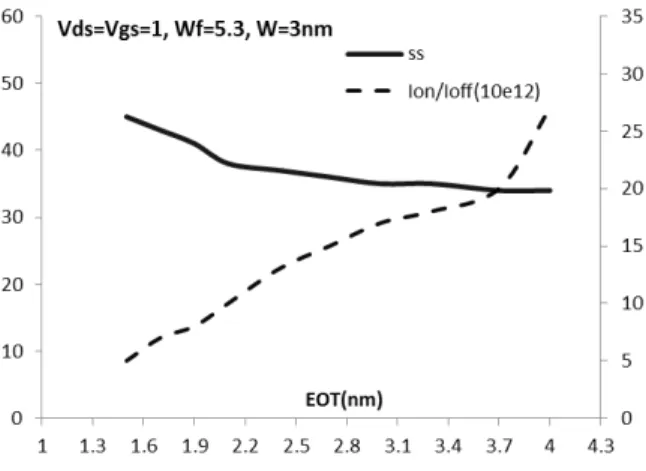
Figure 5 display the input characteristic of the proposed device in the simulation and the analytical model that helps to find the OFF current and SS in the sub-‐threshold region. The analytical model is validated via numerical results obtained from device simulations based on non-‐local band-‐to-‐band tunneling model. It is clearly that the values of Ion and Ioff are around 1×10-‐5 A/µm and 1×10-‐18 A/µm. Figure 6 display the effect of gate oxide thickness on the drain current and sub threshold swing of proposed TFET. It is clearly seen that for small gate oxide thickness, the tunneling current is higher as depicted in figure 6.
Figure 7 shows Ion/Ioff and SS for the In0.35Ga0.65As p-‐n-‐p-‐n TFET with 20 nm gate length
and 3 nm of pocket width as a function of the temperature at VGS = VDS = 1 V. As can be seen, the
off-‐current increases 4 order at high temperature because of thermal generation of carrier in depletion region. It decreases Ion/Ioff, however the variation of temperature is slight effect on the
subthreshold swing.
Different levels of p-‐doping for the source region and n-‐doping for the drain region are shown in Figure 8. The source doping has a high impact on the on-‐current level, since the tunneling takes place between the source and the intrinsic region. The highest-‐possible source doping is acceptable for optimized Tunnel FET operation. Lowering the drain doping lowers the OFF current and sub threshold swing.
In order to demonstrate the effect of mole fraction of In0.35Ga0.65As material on the TFET
performance, the energy band diagrams with different mole fraction are shown in Figure 9. It is observed, Ion is increase and BTBT mechanism has operated properly with mole fraction of 0.85.
In this way, the values of Ion and Ioff are around 1×10-‐5 A/µm and 1×10-‐18 A/µm, respectively at VDS
= 1 V. Therefore, value of Ion/Ioff is 1012 that is remarkable. In addition, the minimum point
subthreshold swing value is about 35 mV/decade. These results indicate that the In0.35Ga0.65As p-‐
n-‐p-‐n TFET has improved device characteristics, including higher Ion and Ion /Ioff; and a steeper
subthreshold swing as compared with the conventional p-‐i-‐n TFET.
Figure 6: Variation of Ion/Ioff and SS for different gate oxide thicknesses.
Figure 7: Ion/Ioff and SS of In0.35Ga0.65As p-‐n-‐p-‐n TFET for various temperatures.
Figure 8: Ion/Ioff of the In0.35Ga0.65As p-‐n-‐p-‐n TFET with 20 nm gate length and 3 nm of pocket width as a function of
Figure 9: The energy band diagram of InxGa1-‐xAs p-‐n-‐p-‐n TFET with different mole fraction.
Table.1: The extracted result of Al0.35Ga0.65As p-‐n-‐p-‐n TFET.
TFET based on III-‐V structure
parameter
35 Subthreshold swing (mV/decade)
2×10-‐5 Ion (A/µm) 3.5×10-‐18 Ioff (A/µm) 0.23 Vth (V) 19.5 Triode slope (mV/decade)
0.13 Saturation slope (mV/decade)
4. CONCLUSION
This paper presented the p-‐n-‐p-‐n TFET based on In0.35Ga0.65As as III-‐V semiconductor
material for further increase both the Ion /Ioff ratio and subthreshold swing of device. Also, an
analytical model is presented for the potential distribution and the drain current of proposed device. The proposed analytical model is validated via numerical results obtained from device simulations based on calibrated nonlocal band-‐to-‐band tunneling model. The proposed structure has p+-‐i-‐n+ structure with a thin δ-‐doped n+ pocket at the source-‐channel interface, low band gap, small tunneling mass, and different band-‐edge alignment induced by the group III-‐V semiconductor. The results show that In0.35Ga0.65As based p-‐n-‐p-‐n TFET shows a higher Ion and
steeper subthreshold swing as compared with the conventional p-‐i-‐n TFET that is expected to be a promising candidate for ultralow power applications and switching devices.
5. REFERENCES
Atlas, D. S. (2010). Atlas User's Manual Silvaco Int. Software. Santa Clara. CA.
Bi, Y., Shamsi, K., Yuan, J. S., Jin, Y., Niemier, M., & Hu, X. S. (2017). Tunnel FET current mode logic for dpa-‐resilient circuit designs. IEEE Transactions on Emerging Topics in Computing, 5(3), 340-‐ 352.
Boucart, K., & Ionescu, A. M. (2007). Double-‐gate Tunnel FET With High K Gate Dielectric. IEEE
Transactions on Electron Devices, 54(7), 1725-‐1733.
Brouzet, V., Salem, B., Periwal, P., Rosaz, G., Baron, T., Bassani, F.. & Ghibaudo, G. (2015). Fabrication and characterization of silicon nanowire pin MOS gated diode for use as p-‐type tunnel FET. Applied Physics A, 121(3), 1285-‐1290.
Chang, H. Y., Adams, B., Chien, P. Y., Li, J., & Woo, J. C. (2013). Improved subthreshold and output characteristics of source-‐pocket Si tunnel FET by the application of laser annealing. IEEE
Transactions on Electron Devices, 60(1), 92-‐96.
Ganapathi, K., & Salahuddin, S. (2011). Heterojunction vertical band-‐to-‐band tunneling transistors for steep subthreshold swing and high on current. IEEE Electron Device Letters, 32(5), 689-‐691.
Gholizadeh, M., & Hosseini, S. E. (2014). A 2-‐D analytical model for double-‐gate tunnel FETs. IEEE
Transactions on Electron Devices, 61(5), 1494-‐1500.
Guo, A., Matheu, P., & Liu, T. J. K. (2011). SOI TFET ION/IOFF Enhancement via Back Biasing. IEEE
Transactions on Electron Devices, 58(10), 3283-‐3285.
Hosseini, S. E., & Moghaddam, M. K. (2015). Analytical modeling of a pnin tunneling field effect transistor. Materials Science in Semiconductor Processing, 30, 56-‐61.
Ionescu, A. M., & Riel, H. (2011). Tunnel field-‐effect transistors as energy-‐efficient electronic switches. nature, 479(7373), 329.
Jhaveri, R., Nagavarapu, V., & Woo, J. C. (2011). Effect of pocket doping and annealing schemes on the source-‐pocket tunnel field-‐effect transistor. IEEE Transactions on Electron Devices,
58(1), 80-‐86.
Kao, K. H., Verhulst, A. S., Vandenberghe, W. G., & De Meyer, K. (2013). Counterdoped pocket thickness optimization of gate-‐on-‐source-‐only tunnel FETs. IEEE Transactions on Electron
Devices, 60(1), 6-‐12.
Khayer, M. A., & Lake, R. K. (2009). Drive currents and leakage currents in InSb and InAs nanowire and carbon nanotube band-‐to-‐band tunneling FETs. IEEE electron device letters, 30(12), 1257-‐ 1259.
Low, K. L., Yeo, Y. C., & Liang, G. (2016). Ultimate performance projection of ultrathin body transistor based on group IV, III-‐V, and 2-‐D-‐materials. IEEE Transactions on Electron Devices,
63(2), 773-‐780.
Marjani, S., & Hosseini, S. E. (2014). Radio-‐frequency modeling of square-‐shaped extended source tunneling field-‐effect transistors. Superlattices and Microstructures, 76, 297-‐314.
Marjani, S., & Hosseini, S. E. (2014, December). RF modeling of pnpn double-‐gate tunneling field-‐ effect transistors. In Millimeter-‐Wave and Terahertz Technologies (MMWATT), 2014 Third
Conference on (pp. 1-‐4). IEEE.
Marjani, S., & Hosseini, S. E. (2014). A novel double gate tunnel field effect transistor with 9 mV/dec average subthreshold slope. In the 22st Iranian Conference on Electrical Engineering
(ICEE), 2014, (pp. 399–402),. IEEE.
Marjani, S., & Hosseini, S. E. (2015). Radio-‐frequency small-‐signal model of hetero-‐gate-‐dielectric pnpn tunneling field-‐effect transistor including charge conservation capacitance and substrate parameters. Journal of Applied Physics, 118(9), 095708.
Marjani, S., Hosseini, S. E., & Faez, R. (2016). A 3D analytical modeling of tri-‐gate tunneling field-‐ effect transistors. Journal of Computational Electronics, 15(3), 820-‐830.
Marjani, S., & Hosseini, S. E. (2015, May). Analysis of radio frequency and stability performance on double-‐gate extended source tunneling field-‐effect transistors. In Electrical Engineering (ICEE),
2015 23rd Iranian Conference on (pp. 1042-‐1046). IEEE.
Marjani, S., Khosroabadi, S. and Hosseini, S. E. (2017). Enhanced characteristics of square-‐shaped extended source TFET via silicon carbide polytype (3C-‐SiC) and a dopant pocket layer. Orient. J.
Chem., 33(3), 1083–1089.
Marjani, S., Hosseini, S. E., & Faez, R. (2016). A silicon doped hafnium oxide ferroelectric p–n–p–n SOI tunneling field–effect transistor with steep subthreshold slope and high switching state current ratio. AIP Advances, 6(9), 095010-‐1–095010-‐7.
Marjani, S., & Hosseini, S. E. (2015). Analyses on radio-‐frequency modeling of double-‐and single-‐ gate square-‐shaped extended source TFETs. Journal of Electrical Systems and Signals, 3(1), 9–14.
Moore, G. E. (1965, January). MOS Transistor as an individual Device and in Integrated Arrays. In
Ieee Spectrum (Vol. 2, No. 3, p. 49). 345 E 47TH ST, NEW YORK, NY 10017-‐2394: IEEE-‐INST
ELECTRICAL ELECTRONICS ENGINEERS INC.
Narang, R., Saxena, M., Gupta, M., & Gupta, R. S. (2011, January). Modeling and simulation of multi layer gate dielectric double gate tunnel field-‐effect transistor (DG-‐TFET). In Students'
Technology Symposium (TechSym), 2011 IEEE (pp. 281-‐285). IEEE.
Salehi, M. R., Abiri, E., Hosseini, S. E., & Dorostkar, B. (2013, May). Analysis and optimization of tunnel FET with band gap engineering. In Electrical Engineering (ICEE), 2013 21st Iranian
Conference on (pp. 1-‐4). IEEE.
Vallett, A. L., Minassian, S., Kaszuba, P., Datta, S., Redwing, J. M., & Mayer, T. S. (2010). Fabrication and characterization of axially doped silicon nanowire tunnel field-‐effect transistors.
Nano letters, 10(12), 4813-‐4818.
Wu, C., Huang, Q., Zhao, Y., Wang, J., Wang, Y., & Huang, R. (2016). A novel tunnel FET design with stacked source configuration for average subthreshold swing reduction. IEEE Transactions
on Electron Devices, 63(12), 5072-‐5076.
Zhao, H., Chen, Y., Wang, Y., Zhou, F., Xue, F., & Lee, J. (2011). InGaAs tunneling field-‐effect-‐ transistors with atomic-‐layer-‐deposited gate oxides. IEEE Transactions on Electron Devices, 58(9), 2990-‐2995.
Zhu, Y., Jain, N., Mohata, D. K., Datta, S., Lubyshev, D., Fastenau, J. M., ... & Hudait, M. K. (2013). Band offset determination of mixed As/Sb type-‐II staggered gap heterostructure for n-‐channel tunnel field effect transistor application. Journal of Applied Physics, 113(2), 024319.