A Dynamic Simulation on Single Gate Junctionless Field Effect
Transistor Based on Genetic Algorithm
Roya Norani1
1
Department of Electrical Engineering, Khorasan Institute of Higher Education University Mashhad, Khorasan Razavi, Iran
Abstract
We study the I-V characteristics of single gate junctionless field effect transistor by device simulation. The sample FET is simulated at different channel lengths and the I-V curve changes due to variations of and channel length have been systematically analyzed. The new approach exhibited here utilizes a Genetic Algorithm to select the important physical and heuristic elements in order to define a compact yet precision model for Single Gate Junctionless Field Effect Transistor characteristic. The results show that the mean absolute percent error (MAPE), root-mean-square deviation (RMSD) and standard deviation error (SDE) were at an acceptable level.
Keywords: Single Gate, Junctionless Field Effect Transistor, Device Simulation, Genetic Algorithm.
1. Introduction
All existing transistors are based on the use of semiconductor junctions formed by introducing dopant atoms into the semiconductor material [1]. In recent years, the devices is designed which have no junctions and were made in n+ or p+ silicon nanowires [1]. They report full CMOS operation of gated resistors and their designed devices have full CMOS functionality, but the new designed contain no junctions or doping gradients. Among emerging devices, nanowire transistors, which could be done with the un-doped or doped body, have drawn much attention for good scaling capability and technology compatibility [2].
Currently, as MOSFET dimensions are scaled down to dozens of nanometers, the short channel effect seriously affects the behavior of devices. In the Nano-scale, the influence of short channel effect on the characteristics of conventional MOSFETs cannot be ignored. To solve this problem, a novel type of MOSFETs, named junctionless field-effect transistors, has been proposed. Compared to conventional inversion-mode MOSFETs, junctionless FETs need no p–n junction to form between regions, which can be seen as n–n–n-type (n-channel) or p–p–p-type (p-channel) junctionless MOSFET devices. It is easier to achieve a good performance of junctionless FETs fabricated on an SOI wafer. Take an n–n–n-type
junctionless FET as an example; it is turned off by piping out the electrons from the body region by the gate electric field force to make the body fully depleted at lower gate bias. The vertical channel of a VMOS is defined by the gate spacer thus the fabrication cost can be reduced drastically. The double-gate scheme of a VMOS helps to increase the gate controllability over the channel region [2]. Thinner silicon films block the channel more easily, and then the channel region achieves complete depletion. From the standpoint of the electric potential distribution, the channel energy band bends due to the reduction of the gate voltage and a strong barrier is formed between the source and drain which makes it difficult for electrons to flow from the source to drain. As the gate bias is increased, the depletion of the body region is eliminated gradually. With the increase of the electron concentration, the resistance also decreases. When the electron concentration reaches body doping concentration ND, the channel region under
provide a more detailed study on its operating characteristics in the situation of short channel effects.
The main purpose of this work is to investigate the characteristics of short channel single gate junctionless FETs by simulations using SILVACO Atlas. There are few methods for estimating the parameters of junctionless transistor that use of optimization techniques. The component which tried to be modeled has same physical properties and these specifications tried to be modeled some mathematical ways [6], [7].
The influence on the devices’ characteristics of changes in
design parameters such as body doping, thickness of silicon body, and channel length has been performed systematically.
2. Properties Simulation
Figure 1 represents the schematic view of a simple single gate junctionless FET. Here, L is the channel length; tb and
tox are the thicknesses of silicon body and gate oxide,
respectively. ND and NA represent the uniform impurity
concentration for n-type and p-type FETs. The channel width is marked as W. The Source and Drain regions and body region of a junctionless FET have the same doping type and concentration. The top of the device has a gate electrode to control the device.
Fig. 1 Schematic view of a simple single gate junctionless FET
3. Mathematical Model
The current in N-JFET due to a small voltage VDS which is, in the linear ohmic region is given by treating the channel
2
(1 GS) DS DSS
P V
I I
V
(2)
Where IDSS is the drain-source saturation current, with this assumption the iD is obtained with VGS=0. We can express
the IDSS as:
2 2
0(1 )
FA FA
DSS DS
I
V
V
V
(3)
In which the parameters are selected as 0=210
-4
A/V2,
VFA=-4 V and =0.01 V-1. Figure 2 shows the characteristic deviation of the drain current ID with gate-to-source voltage VGS forVFAVGS 0.
Fig. 2 ID versus VGS for Constant VDS is shown in this plot
In Figure 3 the ID versus VDS is shown for eight values of
VGS. If the channel impure is monotonous and uniform,
such that the erosion region thickness will grow in proportion to the square root of (the absolute value of) the gate–source voltage, then the channel thickness tb can be expressed in terms of the zero-bias channel thickness a as:
(1 GS ) b
P V t a
V
(4)
Fig. 3 ID versus VDS for Constant VGS is shown in this plot
4. Genetic Algorithm
The Genetic Algorithm (GA) utilizes a non-gradient- based random search and is used in the optimization of complex systems [9]. In the algorithm, each unknown parameter is called gene and each vector of these parameters is called a chromosome [9]. The purpose of the genetic algorithm is to determine the elements of the unknown vector (chromosome) which maximizes or minimizes the defined fitness function [10]. The genetic algorithm is inspired by natural evolution and has population of individuals. In other hand individual is feasible solution to problem each individual is characterized by a Fitness function. In this optimization technique, higher fitness is better solution and based on their fitness, parents are selected to reproduce offspring for a new generation. New generation has same size as old generation; old generation dies and offspring has combination of properties of two parents. So if well designed, population will converge to optimal solution. Genetic algorithms are often applied as an approach to solve global optimization problems. In this paper we have tried to optimize the ID versus VGS. In first step, the flowchart of proposed algorithm in optimization level is shown in figure 4.
The chromosomes in the genetic algorithm are defined as a bit vector with obvious elements, where each bit relates to the model parameters. We use 13 elements where was proposed in [10] as follows:
Chromosome_Vector =
[K m n VTβ k C Vσ WW WVGS p q] (5)
In this vector, if a bit equal to 0, then the corresponding parameter is removed from the proposed model or we can express that n would be replaced by 2, p and q by 1, β, k,
λV, σ, WW and WVGS by zero K, λC and VT by their
physical values. In this algorithm, two main goals have been regarded to define the target function, which are the accuracy and the complexity of the proposed model.
Fig. 4 The steps in genetic algorithm to determine the parameters in junctionless field effect transistor
To consider the first goal in the proposed algorithm, we define the form factor of the proposed model as follows:
max min 2 0 1 _ ( ) ( ) GS DD Model Forcasted DD DS
GS T Max
W V
V
D D
W V
V
W W V V D
Std Dev N N I I I
(6)
Where
I
DModel andI
DForcasted are the drain currents achievedby the compact model (simulated conditions) and the predicted model for same VDS, VGS, and W and IDMax is the
drain current at VDS equal VGS, NW and NVGS are the number
of sampled width and VGS used for calculating standard deviation (Std_ Dev) value [11].
5. Experimental Results
λ Rate 0.95 ND 1.5x1018 cm-3
Crossover Point 0.5 VDS 1.2 V
Mixing Ratio 0.6 VGS 0.2 V to 1.2 V
Initial Gen 13 Body Thickness 10 to 20 nm
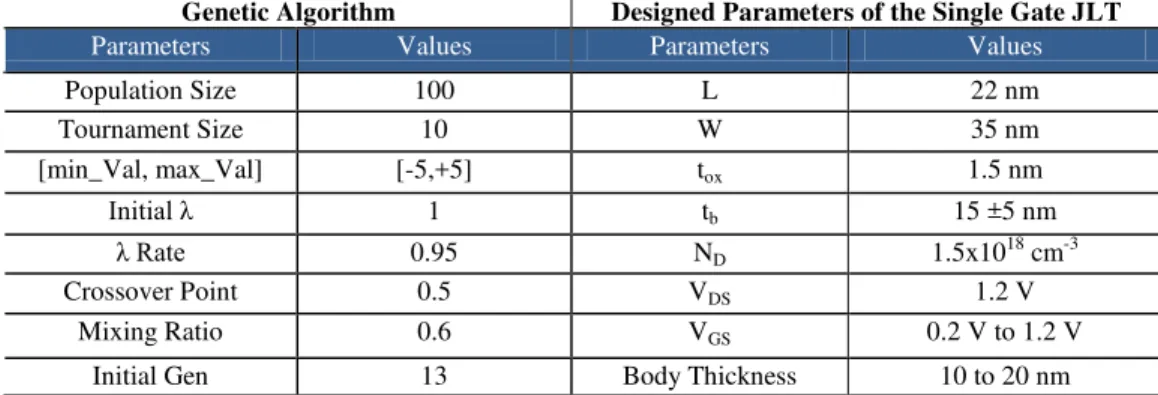
During the simulation, the design parameters of the Single Gate JLT have to be selected as: L = 22 nm, W = 35 nm, tox = 1.5 nm, tb = 15 ±5 nm, ND = 1.5x1018 cm-3, fabricated on a single silicon wafer, using Silicide as the contacts. VDS should be fixed at 1.2 V while the VGS can be varied between 0.2 V to 1.2 V. Set the simple single gate junctionless FET’s parameters as above, and the body thickness shifts from 10 to 20 nm, Figure 6 plots the comparison of the simulation results. Due to each device having the same channel length and width, the control area of the gate is the same. When the body thickness is different, the amount of majority carriers controlled by the gate is also different. Under the same lower gate bias in the sub threshold region, the more majority carriers the devices have, the more difficult it is for the depleted body region to form. Hence the threshold voltage decreases with the increasing of body thickness.
The
MAPE
(Mean
Absolute Percent Error) proposes the size of the error
in percentage terms. It is calculated as the average of
the unsigned percentage error, as shown in the (7):
1
1 N
k k
k k
F A
MAPE
N A
(7)
The root-mean-square deviation (RMSD) is a frequently used measure of the differences between values predicted by a model or an estimator and the values actually observed [12]. Basically, the RMSD represents the sample standard deviation of the differences between predicted values and observed values as (8).
2
1 1
( )
N
k k
k
RMSD F A
N
(8)
Standard deviation error (SDE), according to (9), indicates the persistent error even after calibration of the model.
2
1 1
100 N
k k
k k
F A MAPE SDE
N A
(9)
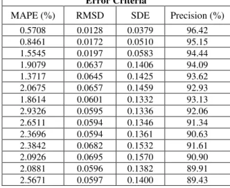
Errors in modeling with considering MAPE, RMSD and
SDE are summarized in Table 2.
Fig. 5 The ID versus VDS is shown that contains characteristic of Single
Fig. 6 Influence of body thickness for simple single gate junctionless FETs. (a) tb = 10 nm, (b) tb = 15 nm and (c)tb = 20 nm
Table 2: Calculation of MAPE, RMSD, SDE and Precision of the proposed technique
Error Criteria
MAPE (%) RMSD SDE Precision (%) 0.5708 0.0128 0.0379 96.42 0.8461 0.0172 0.0510 95.15 1.5545 0.0197 0.0583 94.44 1.9079 0.0637 0.1406 94.09 1.3717 0.0645 0.1425 93.62 2.0675 0.0657 0.1459 92.93 1.8614 0.0601 0.1332 93.13 2.9326 0.0595 0.1336 92.06 2.6511 0.0594 0.1346 91.34 2.3696 0.0594 0.1361 90.63 2.3842 0.0682 0.1532 91.61 2.0926 0.0695 0.1570 90.90 2.0881 0.0596 0.1382 89.91 2.5671 0.0597 0.1400 89.43
6. Conclusion
In this paper the characteristics of a simple single gate junctionless FET was simulated and finally these factors were analyzed. This paper analyzed the influence of body thickness on the threshold voltages and the Drain Current at different Gate voltages. In next step by using Genetic algorithm, one can select between the thirteen proposed model elements based on the precision that needed for a specific objective. For the precision regarded in this paper, only 9 elements were considered and so notified in the simulations.
References
[1] J. P. Colinge, Ch. W. Lee, A. Afzalian, N. Dehdashti Akhavan, R.Yan, I. Ferain, P. Razavi and et al. "Nanowire transistors without junctions", Nature Nanotechnology, 2010, Vol. 5, pp. 225 - 229.
[2] Ch. H. Tai, J. T. Lin, Y. Ch. Eng, and P. Lin, "A Novel High-Performance Junctionless Vertical MOSFET Produced on Bulk-Si Wafer", Solid-State and Integrated Circuit Technology (ICSICT), 2010 10th IEEE International Conference on, 2010, pp. 108-110.
[3] C. Y. Chen, J. T. Lin, M. H. Chiang, and K. Kim, "High-Performance Ultra-Low Power Junctionless Nanowire FET on SOI Substrate in Subthreshold Logic Application", SOI Conference (SOI), IEEE International, 2010, pp 1-2. [4] E. Gnani, A. Gnudi, S. Reggiani, et al. "Theory of the