CENTRO DE TECNOLOGIA
DEPARTAMENTO DE ENGENHARIA METAL ´URGICA E DE MATERIAIS PROGRAMA DE P ´OS-GRADUAC¸ ˜AO EM ENGENHARIA E CIˆENCIA DE
MATERIAIS
FRANCISCO ANDERSON DE SOUSA LIMA
Application of Transition-Metal-Oxide-Based
Nanostructured Thin Films on Third Generation
Solar Cells
Application of Transition-Metal-Oxide-Based
Nanostructured Thin Films on Third Generation
Solar Cells
Thesis submitted to the Graduate Program in Ma-terials Science and Engineering in partial fulfillment of the requirements for the degree of Doctor in Ma-terials Science and Engineering. Concentration area: Physical and Mechanical Properties of Materials. Advisors: Prof. Dr. Igor Frota de Vasconcelos
Prof. Dr. M´onica Lira-Cant´u
Biblioteca de P´os-Gradua¸c˜ao em Engenharia - BPGE
L698a Lima, Francisco Anderson de Sousa.
Application of transition-metal-oxide-based nanostructured thin films on third gener-ation solar cells / Francisco Anderson de Sousa Lima. – 2015.
247 f. : il. color. , enc. ; 30 cm.
Tese (doutorado) - Universidade Federal do Cear´a, Centro de Tecnologia, Depar-tamento de Engenharia Metal´urgica e de Materiais, Programa de P´os-Gradua¸c˜ao em Engenharia e Ciˆencia de Materiais, Fortaleza, 2015.
´
Area de Concentra¸c˜ao: Propriedades F´ısicas e Mecˆanicas dos Materiais Orienta¸c˜ao: Prof. Dr. Igor Frota de Vasconcelos
Coorienta¸c˜ao: Prof. Dr. M´onica Lira-Cant´u
1. Ciˆencia dos materiais 2. Filmes finos. 3. Eletrodeposi¸c˜ao. 4. C´elulas solares. I. T´ıtulo.
One of the greatest challenges of our time is to devise means to provide energy in a sustainable way to attend an exponentially growing demand. The energy demand is expected to grow 56% by 2040. In this context, the use of clean and sustainable sources of energy is imperative. Among these sources, solar energy is the only one which can meet the total world energy requirement even considering such large growth in demand. The solar power incident on the Earth’s surface every second is equivalent to 4 trillion 100-watt light bulbs. Photovoltaic solar cells are one of several ways to harness solar energy. These cells convert solar energy directly into electricity. Commercial photovoltaic devices are already a reality, but their share of the world energy matrix is still quite small, mainly due to the high costs. Next generation photovoltaics open a number of new possibilities for photovoltaic energy applications that can potentially decrease the overall cost of energy production. Transition metal semiconductor oxides are promising materials that can be produced by low cost methods and offer interesting new features. The use of these materials in next generation photovoltaics is therefore a very promising and interesting application. In this thesis work zinc, titanium and vanadium oxides were used in next generation solar cells. Thin films of zinc oxide were synthesized by the low cost and environmentally friendly techniques of electrodeposition and hydrothermal synthesis and applied as working electrodes in highly efficient dye sensitized solar cells (DSSCs). The films were characterized by structural and optical techniques while the cells were tested by currentvs.voltage and quantum efficiency measurements. The efficiencies of these cells were as high as 2.27% using ZnO thin films without any post deposition treatment. Moreover, natural dyes extracted from plants of northeastern Brazil were applied as sensitizers in DSSCs assembled with commercial available TiO2 as working
electrode. The natural dyes were extracted employing very simple methods and were characterized by XPS and UPS techniques. Their band alignments were shown to be compatible with the TiO2 as well as with the mediator electrolyte. The efficiency of
DSSCs sensitized with natural dyes were as high as 1.33%. Finally, water based V2O5
was used as hole transport medium (HTM) in conventional organic solar cells (OSCs) and ITO-free, plastic OSCs. The results obtained with V2O5 were compared with the results
obtained from cells assembled with PEDOT:PSS, which is the most used HTM. This comparison showed that the use of V2O5 as HTM can lead to more efficient OSCs. The
stability of these devices were evaluated by tests applying the ISOS standards ISOS-D-1, ISOS-L-1 and ISOS-O-1. A UV-filter and a protective graphene oxide (GO) layer were employed seeking to improve the stability of OSCs. The combination of both UV-filter and GO protective layer was shown to be the most effective way to improve the stability of these devices.
Um dos maiores desafios do nosso tempo ´e desenvolver formas para fornecer energia de forma sustent´avel para atender uma demanda que cresce exponencialmente e que dever´a crescer 56% at´e 2040. Neste contexto, o uso de fontes limpas e sustent´aveis de energia ´e um imperativo. Entre essas fontes, a energia solar ´e a ´unico que pode satisfazer a ne-cessidade total de energia do mundo, mesmo considerando o crescimento na demanda. A potˆencia solar incidente na superf´ıcie da Terra a cada segundo ´e equivalente a 4 trilh˜oes de lˆampadas de 100 watts. C´elulas solares fotovoltaicas s˜ao uma das v´arias maneiras de aproveitar a energia solar, convertendo-a diretamente em eletricidade. Dispositivos com-erciais fotovoltaicos j´a s˜ao uma realidade, mas a sua participa¸c˜ao na matriz energ´etica mundial ainda ´e muito pequena, principalmente devido aos seus custos elevados. C´elulas fotovoltaicas de nova gera¸c˜ao abrem uma s´erie de novas possibilidades para aplica¸c˜oes de energia fotovoltaica que pode diminuir o custo total de produ¸c˜ao de energia. ´Oxidos semicondutores de metais de transi¸c˜ao s˜ao materiais promissores que podem ser produzi-dos atrav´es de m´etoproduzi-dos de baixo custo e que possuem caracter´ısticas interessantes. Por conseguinte, o uso destes materiais em energia fotovoltaica de pr´oxima gera¸c˜ao se apre-senta com uma aplica¸c˜ao promissora. Nesta tese de doutorado ´oxidos de zinco, titˆanio e van´adio foram utilizados em c´elulas solares de pr´oxima gera¸c˜ao. Filmes finos de ´oxido de zinco foram sintetizados por eletrodeposi¸c˜ao e s´ıntese hidrot´ermica. Os filmes foram apli-cados como eletrodos de trabalho em c´elulas solares sensibilizadas por corante (DSSCS) altamente eficientes. Os filmes foram caracterizados por t´ecnicas estruturais e ´oticas en-quanto que as c´elulas foram testadas por medidas de correntevs.voltagem e de eficiˆencia quˆantica. A eficiˆencia dessas c´elulas atingiu 2,27% utilizando filmes finos de ZnO sem qualquer tratamento p´os-deposi¸c˜ao. Al´em disso, corantes naturais extra´ıdos de plan-tas do nordeste do Brasil foram aplicados como sensibilizadores em DSSCs montadas com TiO2 comercial utilizado como eletrodo de trabalho. Os corantes naturais foram extra´ıdas
empregando m´etodos simples e foram caracterizados por espectroscopia de fotoel´etrons excitados por raios X e por radia¸c˜ao ultravioleta, XPS e UPS respectivamente. Seus alin-hamentos de banda se mostraram compat´ıveis com o TiO2e com o eletrodo de regenera¸c˜ao.
A eficiˆencia das DSSCs sensibilizadas com corantes naturais chegou a 1,33%. Finalmente, V2O5 `a base de ´agua foi usado como material transportador de buracos (HTM) em c´elulas
solares orgˆanicas (OSCs) convencionais e OSCs de pl´astico constru´ıdas sem ITO. Os re-sultados obtidos com V2O5 foram comparados com os resultados de c´elulas constru´ıdas
com PEDOT:PSS, que ´e o HTM mais utilizado. Esta compara¸c˜ao revelou que o uso de V2O5 como HTM pode levar a OSCs mais eficientes. A estabilidade destes dispositivos
foi avaliada por testes aplicando os padr˜oes ISOS-D-1, ISOS-L-1 e ISOS-O-1. O uso de filtros ultravioleta e de uma camada protetora de ´oxido de grafeno reduzido foi testado com o intuito de melhorar a estabilidade desses dispositivos. O uso de uma combina¸c˜ao de ambos se mostrou a forma mais efetiva de melhorar a estabilidade das OSCs.
2.1 Total primary power density supply from sunlight. . . 7
2.2 World energy production by source in 2012. . . 8
2.3 Potential energy production per year of various types of renewable energy sources. . . 9
2.4 Global photovoltaic cumulative installed capacity share in 2012 (MW; %). 10 2.5 Total irradiance on the horizontal plane on Germany (left) and on Brazil (right). . . 11
2.6 Solar spectrum at the top of the atmosphere and sea level. . . 12
2.7 Solar spectrum at the top of the atmosphere and sea level. . . 13
2.8 Schematic representation of indirect and direct energy band gap transitions. 19 2.9 Schematic representation of a simple conventional solar cell. . . 21
2.10 Schematic representation circuit of a photovoltaic cell. . . 23
2.11 Example of a typicalJ −V curve for a solar cell. . . 25
2.12 Effect of the modification of series resistance and shunt resistance inJ−V curves of a solar cell. . . 26
2.13 Schematic overview of the exciton formation by the absorption of the light. 31 2.14 Schematic overview of the exciton formation in a molecule. . . 32
2.15 Schematic overview of a dye-sensitized solar cell. . . 34
2.16 Basic electron transfer process occurring within a DSSC. . . 35
2.17 Schematic representation of single layer, bilayer and bulk heterojunction organic solar cells. . . 37
2.18 Schematic energy level diagram of a typical bilayer organic solar cell. . . . 39
2.19 Normal and inverted architecture bulk heterojunction solar cells. . . 41
2.20 Absorption and thermalization losses in a organic solar cell. . . 41
2.21 Film absorption of two polymers with different band gaps in a blend with PCBM. . . 42
2.22 Tandem OSCs with normal and inverted architectures. . . 43
2.23 Band alignment for different TMOs with photovoltaic polymers and electron-accepting fullerene derivatives. . . 47
2.24 Comparison between the stability of organic solar cells. . . 47
2.25 Stick-and-ball representation of ZnO crystal structures. . . 50
2.26 Stick-and-ball representation of TiO2 crystal structures. . . 51
2.27 Crystallization of V2O5 thin films. . . 53
3.1 The X-ray diffraction of crystallographic planes. . . 74
3.2 Pear-shaped volume probed by different microprobe signals. . . 78
3.3 XPS setup. . . 79
4.1 Experimental set up for the electrodeposition of ZnO thin films. . . 88
4.4 The SEM micrographs of electrochemically deposited ZnO electrodes. . . . 95 4.5 The SEM micrographs for ZnO electrodes electrochemically deposited at
different electrolyte concentrations. . . 97 4.6 High-resolution SEM micrographs for electrodeposited ZnO thin films. . . . 98 4.7 The TEM micrograph for an electrochemically deposited ZnO electrode. . . 99 4.8 An overview of the XPS results for electrodeposited ZnO thin films. . . 101 4.9 high-resolution XPS results for electrodeposited ZnO thin films. . . 102 4.10 Valence band UPS spectrum for an electrodeposited ZnO thin film. . . 103 4.11 Details of valence band edge and secondary electron cutoff obtained for an
electrodeposited ZnO thin film . . . 104 4.12 Tauc’s plot: calculation of bandgap of electrodeposited ZnO thin film. . . . 105 4.13 Band diagram for an electrodeposited ZnO thin film. . . 106 4.14 Band alignment for a DSSC using electrochemically deposited ZnO as a
working electrode. . . 107 4.15 J−V curves and IPCE spectra for DSSCs assembled with five samples of
electrodeposited ZnO thin films. . . 108 4.16 Dye desorption study for DSSCs assembled with electrochemically deposited
ZnO. . . 110 4.17 J − V curves and IPCE spectra for the cell that presents a significant
improvement in performance after aging under ambient conditions. . . 111 4.18 Time evolution of the photovoltaic parameters under ambient conditions
for a DSSC assembled with electrodeposited ZnO. . . 112 5.1 Schematic representation of the growth of ZnO nanorods on ITO substrates
using hydrothermal synthesis from an initial layer of ZnO nanoparticles. . . 123 5.2 Experimental set up for the growth of ZnO nanorod thin films. . . 125 5.3 XRD diffractograms for hydrothermally synthesized ZnO thin films. . . 128 5.4 Comparison of XRD results for hydrothermally synthesized and
electro-chemically deposited ZnO thin films. . . 129 5.5 Raman spectrum for hydrothermally synthesized ZnO thin films. . . 130 5.6 Raman spectra comparions for hydrothermally synthesized and
electro-chemically deposited ZnO thin films. . . 130 5.7 SEM images for the hydrothermally synthesized and electrodeposited thin
films. . . 131 5.8 TEM images for a hydrothermally synthesized ZnO NR. . . 132 5.9 An overview of the XPS results for hydrothermally synthesized ZnO thin
films. . . 133 5.10 High-resolution XPS results for hydrothermally synthesized ZnO thin films. 134 5.11 Comparison between the valence band UPS spectra for ZnO thin films
deposited by hydrothermal synthesis and electrochemical deposition. . . 135 5.12 Details of the secondary electron cutoff and valence band edge obtained for
hydrothermally synthesized ZnO thin films. . . 136 5.13 Comparison between the optical bandgaps for ZnO thin films deposited by
hydrothermal synthesis and electrochemical deposition. . . 137 5.14 Band diagram for hydrothermally synthesized and electrodeposited ZnO
chemically deposited ZnO as working electrodes. . . 138 5.16 J−V curve and IPCE spectra for the best devices using ZnO synthesized
by hydrothermal synthesis assembled with different FTO substrates. . . 139 5.17 J −V curves and normalized PCE for the dye loading time study. . . 140 5.18 Comparison betweenJ−V curves for devices assembled with ZnO working
electrodes prepared by hydrothermal synthesis and electrochemical depo-sition. . . 141 6.1 UV-Vis absorption spectra of the extracts from the three natural dyes used
as sensitizers in DSSCs. . . 153 6.2 Tauc’s plot for the natural dyes used as sensitizers in DSSCs. . . 154 6.3 Valence band UPS spectra for the natural dyes used as sensitizers in DSSCs.155 6.4 Band alignment diagrams for the natural dyes used as sensitizers in DSSCs. 156 6.5 J −V curves for the DSSCs sensitized with the three natural dyes. . . 158 6.6 IPCE spectra for the DSSCs sensitized with the three natural dyes. . . 159 7.1 Structure of the ITO-Free flexible OPV. . . 165 7.2 LBG polymer P10 was used as active material for the second active layer. . 166 7.3 Mini-roll coater used to fabricate ITO-free, plastic OSCs. . . 167 7.4 Effect of the thickness variation of V2O5 on the PCE of organic solar cells. 170
7.5 Comparison between PEDOT:PSS and V2O5 as HTL in plastic organic
solar cells. . . 172 7.6 Light-beam induced-current image for the best OSCs with V2O5 as the HTL.172
7.7 J −V curve and IPCE spectrum for the best OSC with V2O5 as the HTL. 173
7.8 Effect of the use of highly conductive PEDOT:PSS as part of the back electrode in plastic organic solar cells. . . 174 7.9 Comparison between water-based V2O5 and ViPr-based V2O5 as HTL in
plastic solar cells. . . 175 7.10 XPS survey for two different V2O5 thin films. . . 176
7.11 High-resolution XPS spectra of the V 2p and O 1s core-levels for two dif-ferent V2O5 thin films. . . 177
7.12 Valence band UPS spectra for two different V2O5 thin films. . . 179
7.13 Optical microscopy images for the V2O5 thin film in the normal OSC
con-figuration. . . 180 7.14 Comparison between water-based V2O5 and PEDOT:PSS as HTL in
nor-mal configuration plastic solar cells. . . 181 7.15 Optical microscopy images for the V2O5 thin film for the normal OSC
configuration on top of silver nanowires. . . 182 7.16 J −V curve for normal configuration OSCs. . . 182 7.17 J −V curve and IPCE spectrum for a TPSC using V2O5 as part of the
recombination layer. . . 184 8.1 J −V curves for OSCs before and after an aging time of 90 days inside a
glove box. . . 194 8.2 J −V curves, for best performing, OSCs aged in air for 60 days without
erated degradation test (solar simulator conditions) for 72 h, according to the ISOS-L-1 standard. . . 197 8.4 J −V curves for OSCs degradation tests under solar simulator conditions
over 72 h, according to the ISOS-L-1 standard. . . 198 8.5 Time evolution of the photovoltaic parameters for two OSCs tested under
real outdoor conditions over 1000 h, according to the ISOS-O-1 standard. . 200 8.6 J −V curves for OSCs degradation tests under real outdoor conditions,
according to the ISOS-O-1 standard. Insets show IPCE spectra. . . 201 8.7 Time evolution of the photovoltaic parameters of plastic OSCs under real
outdoor degradation tests using V2O5 or PEDOT:PSS as HTL, according
to the ISOS-O-1 standard. . . 202 8.8 Comparison between the PCE evolution for plastic OSCs under real
out-door degradation tests using V2O5 or PEDOT:PSS as HTL, according to
the ISOS-O-1 standard. . . 203 8.9 J −V curves for plastic OSCs under real outdoor degradation tests using
V2O5 or PEDOT:PSS as HTL, according to the ISOS-O-1 standard. . . 204
8.10 Time evolution of the photovoltaic parameters for OSCs without UV filter with UV filter during real outdoor degradation tests according to the ISOS-O-1 standard. . . 206 8.11 J−V curves for OSCs degradation tests, without and with UV filter, under
real outdoor conditions, according to the ISOS-O-1 standard. . . 207 8.12 J −V curves and IPCE spectra for OSCs degradation test, without UV
filter, obtained under solar simulator conditions before and after the ISOS-O-1 2500-h stability test. The inset shows normalized IPCE spectra. . . 208 8.13 J−V curves and IPCE spectra for OSCs degradation tests, with UV filter,
obtained under solar simulator conditions before and after the ISOS-O-1 2500-h stability test. The inset shows normalized IPCE spectra. . . 209 8.14 J−V curves for OSCs degradation tests, without and with a GO protective
layer, under real outdoor conditions, according to the ISOS-O-1 standard. . 210 8.15 Time evolution of the photovoltaic parameters for OSCs degradation tests,
without and with a GO protective layer, under real outdoor conditions, according to the ISOS-O-1 standard. . . 211 8.16 J −V curves and IPCE spectra for OSCs degradation tests with a GO
protective layer under solar simulator conditions, before and after the ISOS-O-1 2500-h stability test. The inset shows normalized IPCE spectra. . . 212 8.17 Comparison between the time evolution of PCE for OSC with and without
a GO protective layer. . . 213 8.18 J−V curves for OSCs degradation tests, without and with a combination of
UV filter and GO protective layer, under real outdoor conditions, according to the ISOS-O-1 standard. . . 214 8.19 Time evolution of the photovoltaic parameters for OSCs degradation tests
without and with a combination of UV filter and GO protective layer, under real outdoor conditions, according to the ISOS-O-1 standard. . . 215 8.20 J−V curves and IPCE spectra for OSCs degradation tests with a
2.1 Samples and deposition conditions. . . 48 2.2 General physical properties of ZnO semiconductor material. . . 49 4.1 Samples and deposition conditions for the electrodeposited ZnO thin films. 91 4.2 EDX results for the composition of electrodeposited ZnO electrodes. . . 100 4.3 XPS results for the composition of electrodeposited ZnO electrodes. . . 102 4.4 Photovoltaic parameters for DSSCs assembled with electrochemically
de-posited ZnO. . . 109 5.1 XPS results for the composition of hydrothermally synthesized ZnO
elec-trodes. . . 133 5.2 Photovoltaic parameters for DSSCs assembled with hydrothermally
syn-thesized ZnO on different FTO substrates. . . 139 5.3 Photovoltaic parameters for DSSC assembled with electrochemically
de-posited and hydrothermally synthesized ZnO. . . 142 7.1 Photovoltaic parameters for ITO-free OSCs: PEDOT:PSS or V2O5 as HTL. 170
7.2 Comparison of the photovoltaic parameters for OSCs with and without highly conductive PEDOT. . . 174 7.3 Binding energy values of the main peaks in the XPS spectra for the two
different V2O5 thin films. . . 178
7.4 Comparison of the photovoltaic parameters for OSCs in normal configura-tion with PEDOT:PSS or V2O5 as HTL. . . 180
8.1 Average photovoltaic parameters of OSCs before and after an aging time of 90 days inside a glove box. . . 195 8.2 Average photovoltaic parameters of OSCs aged in air for 60 days without
and with encapsulation, according to the ISOS-D-1 standard. . . 196 8.3 Photovoltaic parameters for OSCs degradation tests under solar simulator
conditions over 72 h, according to the ISOS-L-1 standard. . . 199 8.4 Photovoltaic parameters for OSCs degradation tests under real outdoor
conditions, according to the ISOS-O-1 standard. . . 201 8.5 Photovoltaic parameters for OSCs degradation tests, without and with UV
filter, under real outdoor conditions, according to the ISOS-O-1 standard. . 207 8.6 Photovoltaic parameters for OSCs degradation tests, without and with UV
filter, obtained under solar simulator conditions, before and after the ISOS-O-1 2500-h stability test. . . 209 8.7 Photovoltaic parameters for OSCs degradation tests, without and with a
TMO Transition metal oxide TFPV Thin film photovoltaics
TFT Thin film transistor FET Field effect transistor LED Ligth emitted diode
BIPV Building integrated photovoltaics ZnO Zinc oxide
TiO2 Titanium dioxide
V2O5 Vanadium pentoxide
DSSC Dye sensitized solar cell OSC Organic solar cell
SEM Scanning electron microscopy TEM Transmission electron microscopy UV-Vis Ultraviolet–visible spectroscopy
XRD X-ray diffraction
EDX Energy dispersive X-ray spectroscopy XPS X-ray photoelectron spectroscopy UPS Ultraviolet photoelctron spectroscopy J−V Current-voltage
IPCE Incident photon to collected electron efficiency ITO Indium doped tin oxide
FTO Fluorine doped tin oxide IEA International Energy Agency
IR Infrared AM Air mass
e.m.f. Electron motive force EC Conduction band
EV Valence band
EG Forbidden energy band gap
EF Fermi level
T Absolute temperature K Boltzmann constant
NC Density of states in the conduction band
NV Density of states in the valence band
n Electron density p Hole density
ND Donor concentration
NA Acceptor concentration
n Electron density
IL Light generated current
ID Voltage dependent current lost
Ish Current lost due to shunt resistance
I0 Saturation current
Rs Series resistance
A Ideality factor VT Thermal voltage
Rs Series resistance
Tc Cell’s working temperature
Rs Shunt resistance
Voc Open circuit voltage
Pmax Maximum power density
Vmax Maximum open circuit voltage
Jmax Maximum short circuit current density
F F Fill factor
η Solar cell efficiency
EQE External quantum efficiency
IPCE Incident photon to collected electron efficiency TCO Transparent conductive oxide
Nc Number of generated charges
Nf Number of incident photons per unit time
Iλ Intensity of the source
Nc Number of generated charges
AM Air mass
OPV Organic photovoltaic XSC Excitonic solar cell CdTe Cadmium teluride
CIGS Copper indium gallium selenide CZTS Copper zinc tin sulfide
CZTS Copper zinc tin selenide CIS Copper indium selenide EBE Exiton binding energy
DA Donor acceptor interface CT Charge transfer
HOMO Highest occupied molecular orbital LUMO Lower unoccupied molecular orbital
BHJ Bulk heterojunction
ηA Quantum efficiency for exciton generation
ηCT Quantum efficiency for exciton separation
µ Mobility
ηCC Quantum efficiency for charge collection
NP Nanoparticle
P3HT Poly(3-hexylthiophene-2,5-diyl)
PCBM [6,6]-phenyl-C61-butyric acid methyl ester
PEDOT:PSS Poly(3,4-ethylenedioxythiophene) polystyrene sulfonate MoO3 Molybdenum oxide
HTL Hole transport layer ETL Electron transport layer
F Faraday constant R Gas constant
p Pressure
Ik Bragg intensity
Fk Structure factor
TEM Transmission electron microscopy h Planck’s constant
SEM Scanning electron microscopy SAED Selected-area electron diffraction
BF Bright field DF Dark field
HREM High-resolution electron microscopy imaging KE Kinetic energy
BE Biding energy φ Work function Z Atomic number
α Absorption coefficient WE Working electrode
CE Counter electrode RE Reference electrode
EBPVD Electron beam physical vapor deposition LO Longitudinal-optical
TO Transversal-optical NR Nanorod
HMT Hexamethylenetetramine ED Electrodeposited
HS Hydrothermally synthesized LP Lower biding energy peak MP Medium biding energy peak
HP High biding energy peak
LC FTO Less conductive fluorine doped tin oxide MC FTO More conductive fluorine doped tin oxide
HC-P Highly conductive PEDOT:PSS LBG Low bang gap
LBIC Light-beam Induced-current
ICN2 Institut Catal`a de Nanoci´encia i Nanotecnologia DTU Danmarks Tekniske Universitet
TPSC Tandem polymer solar cell R2R Roll-to-roll
PREFACE . . . 1
1. INTRODUCTION AND OBJECTIVES . . . 3
1.1 Objectives . . . 4
1.2 Outline . . . 5
2. SOLAR CELLS . . . 7
2.1 Solar cells: general aspects . . . 7
2.1.1 The importance of solar energy . . . 7
2.1.2 Solar spectrum . . . 11
2.1.3 A brief history of the photovoltaic technology . . . 13
2.1.4 Physical principles . . . 14
2.1.5 Semiconductors . . . 15
2.1.5.1 Properties of semiconductors . . . 16
2.1.5.2 p−n junctions . . . 20
2.1.5.3 Solar cells operation . . . 21
2.1.6 Characterization techniques . . . 22
2.1.6.1 Current density vs. voltage: J −V curves . . . 22
2.1.6.2 External quantum efficiency . . . 26
2.1.7 Thin Film Photovoltaics . . . 28
2.1.7.1 Excitons . . . 30
2.1.7.2 Dye sensitized solar cells . . . 32
2.1.7.3 Organic solar cells . . . 36
2.2 Transition metal oxides for next generation solar cells . . . 43
2.2.1 Why transition metal oxides for next generation solar cells? . . . . 44
2.2.2 Introduction to transition metal oxides . . . 46
2.2.3 Zinc oxide (ZnO) . . . 48
2.2.4 Titanium dioxide (TiO2) . . . 50
2.2.5 Vanadium oxide (V2O5) . . . 51
2.2.6 Synthesis of oxide semiconductors . . . 53
2.2.6.1 Electrodeposition . . . 53
2.2.6.2 Hydrothermal synthesis . . . 55
2.2.6.3 Sol-gel . . . 56
2.3 References . . . 57
3. CHARACTERIZATION TECHNIQUES . . . 73
3.1 X-ray diffraction . . . 73
3.2 Electron microscopy . . . 74
3.4.1 X-ray photoelectron spectroscopy . . . 78
3.4.2 Ultraviolet photoelectron spectroscopy . . . 80
3.5 Ultraviolet-visible absorption spectroscopy . . . 81
3.6 Raman spectroscopy . . . 82
3.7 References . . . 83
4. ELECTRODEPOSITED ZINC OXIDE THIN FILMS FOR DYE SENSITIZED SOLAR CELLS . . . 84
4.1 Introduction . . . 84
4.2 Water-based fabrication of ZnO . . . 85
4.2.1 Electrodeposition of ZnO . . . 86
4.2.2 Practical matters . . . 87
4.3 Experimental procedure . . . 87
4.3.1 Synthesis of nanostructured ZnO thin films . . . 87
4.3.2 Structural, morphological and electrical characterization of the films 89 4.3.3 Solar cell fabrication and characterization . . . 90
4.4 Structural, morphological, compositional, and electrical analysis . . . 90
4.4.1 X-ray diffraction . . . 91
4.4.2 Raman spectroscopy . . . 92
4.4.3 Electron microscopy . . . 94
4.4.4 Energy dispersive X-ray spectroscopy . . . 99
4.4.5 X-ray photoelectron spectroscopy . . . 100
4.4.6 Band diagram . . . 103
4.5 Photovoltaic performance . . . 107
4.6 Conclusions . . . 113
4.7 References . . . 113
5. HYDROTHERMALLY SYNTHESIZED ZINC OXIDE THIN FILMS FOR DYE SENSITIZED SOLAR CELLS . . . 121
5.1 Introduction . . . 121
5.2 Hydrothermal synthesis of ZnO . . . 122
5.3 Experimental procedure . . . 124
5.3.1 Synthesis of ZnO nanorod thin films . . . 124
5.3.2 Structural, morphological and electrical characterization of the films 125 5.3.3 Solar cell fabrication and characterization . . . 126
5.4 Structural, morphological, compositional, and electrical analysis . . . 127
5.4.1 X-ray diffraction . . . 127
5.4.2 Raman spectroscopy . . . 128
5.4.3 Electron microscopy . . . 131
5.4.4 X-ray photoelectron spectroscopy . . . 132
5.4.5 Band diagram . . . 134
5.5 Photovoltaic performance . . . 138
5.5.1 Comparison between hydrothermally synthesized and electrodeposited ZnO thin films as working electrodes in DSSCs . . . 140
5.6 Conclusions . . . 143
6.1 Introduction . . . 149
6.2 Experimental procedure . . . 151
6.2.1 Preparation of dye sensitizer solutions . . . 151
6.2.2 Preparation of electrodes . . . 151
6.2.3 DSSC assembly . . . 152
6.2.4 Characterization . . . 152
6.3 Results and discussion . . . 153
6.3.1 Light absorption by natural dyes . . . 153
6.3.2 Determination of the HOMO and LUMO levels of the natural dyes 154 6.3.3 Band diagram . . . 156
6.3.4 Photovoltaic performance . . . 157
6.4 Conclusions . . . 158
6.5 References . . . 159
7. VANADIUM PENTOXIDES FOR ITO-FREE PLASTIC ORGANIC SOLAR CELLS . . . 163
7.1 Introduction . . . 163
7.2 Experimental . . . 164
7.2.1 Materials . . . 164
7.2.2 Coating procedure . . . 167
7.3 Application of water-based V2O5 in flexible ITO-free OPVs . . . 169
7.3.1 Comparison between V2O5 and PEDOT:PSS as HTL for ITO-free plastic OPVs . . . 169
7.3.2 Comparison between water-based V2O5 and ViPr-based V2O5 as the HTL for ITO-free plastic OPVs . . . 173
7.3.3 Application of V2O5 as HTL in normal configuration, ITO-free flex-ible OPVs . . . 179
7.3.4 Application of V2O5 as part of the recombination layer in tandem OPVs . . . 183
7.4 Conclusions . . . 184
7.5 References . . . 184
8. STABILITY OF ORGANIC SOLAR CELLS . . . 191
8.1 Introduction . . . 191
8.2 Experimental . . . 192
8.2.1 Sample preparation . . . 192
8.2.2 Stability tests . . . 193
8.3 Results and discussion . . . 194
8.3.1 Degradation under inert atmosphere in dark . . . 194
8.3.2 Degradation of OSCs according to the ISOS-D-1 standard . . . 195
8.3.3 Degradation of OSCs according to the ISOS-L-1 standard . . . 196
8.3.4 Degradation of OSCs according to the ISOS-O-1 standard . . . 199
8.3.4.1 V2O5 vs. PEDOT:PSS . . . 202
8.3.5 Strategies for improving the stability of OSCs . . . 204
8.3.5.1 UV filter . . . 205
PREFACE
This doctoral thesis was developed in partnership between the Graduate Program in Materials Science and Engineering of Universidade Federal do Cear´a (UFC) and the Cata-lan Institute of Nanoscience and Nanotechnology (ICN2) of the Universitat Aut`onoma de Barcelona (UAB). The thesis work was directed by Prof. Igor Frota de Vasconcelos of UFC and Prof. M´onica Lira-Cant´u of ICN2-UAB.
My first year in the program was spent in UFC attending courses and developing the idea for the research project. Some preliminary research work was done during this first year. The next two years were spent in ICN2 doing the core of the research work. The first year in Barcelona was financed by the Brazilian Research Council (CNPq) through a fellowship within the Science Without Borders program while the second year was financed by ICN2. My last few months were spent in UFC where I devoted my time to finish writing this thesis. This work was also partially funded by the Research Support Foundation of the State of Cear´a (FUNCAP) through FUNCAP’s International Cooperation Program.
· · · ·
I would like to thank CNPq, FUNCAP and ICN2 for the financial support mentioned above, without which I would not have been able to finish this work. I also would like to thank UFC and the Graduate Program in Materials Science and Engineering for the opportunity to purse a doctorate degree.
I am also extremely grateful to Dr. Monica Lira-Cantu for her generosity in giving me so many opportunities to learn, apply new knowledge and to participate in many new projects. Also by always willing to discuss new ideas and results and for trusting me by giving me autonomy and responsibilities which helped me develop new skills that are being very useful in my career.
I have been very lucky for having two advisors. I have to say an enormous thank you to Prof. Igor Frota de Vasconcelos for his always valuable lessons and discussions, his commitment to my education, his great help in the preparation of documents written and for always being open to new ideas.
I would like to thank the members of the committee Prof. Ana Fl´avia Nogueira, Prof. Alexandre Magno Rodrigues Teixeira, Prof. Pedro de Lima Neto, and Prof. Pierre Bas´ılio Almeida Fechine for their valuable time.
I also would like to thank to my friends who have helped me during this journey. Oliveira Junior, Mauricio, and Kleyton of UFC for the help with the heavy courses; Thiago, Iran, and Gislania of UFC for the very interesting discussions; Irene and Gerardo of ICN2 for the help on my first contact with the next generation solar cells; Raphael and Aurelie for the good reception and the help in using the new equipment; Fernando and Andressa for the fruitful talks; Amador for the big number of good suggestions; Guillaume for the patience and the help with XPS and UPS.
1. INTRODUCTION AND OBJECTIVES
Transition metal oxides (TMOs), from the simplest binary oxides to the more com-plex oxide compounds, are a class of materials with great variety of functional properties. These span from insulating, semiconducting or metallic behavior, to ferroelectricity, mag-netism, magneto resistance or superconductivity, among many more. TMOs are now regularly applied in many printed electronic and optoelectronic devices such as thin film photovoltaics (TFPVs), thin film and field effect transistors (TFTs and FETs respec-tively), light emitting diodes (LEDs), etc. Common to most of these devices are their maturity with respect to novel materials and high performance. The attention is also directed to their manufacture, which include large-scale, large-volume, flexible and recy-clable, disposable and/or reusable devices. Novel deposition techniques are used to obtain high structural quality, which is slowly reaching that observed for conventional deposition methods (vacuum-based or similar). This is especially true for TFPVs (organic solar cells, polymer/oxide solar cells, all-oxide solar cells, perovskite solar cells, mesoscopic dye solar cells, quantum-dot solar cells) where large-scale, large volume applications allow low cost fabrication and the possibility to be competitive at the commercial level. In addition, oxide semiconductors can also confer higher lifetime stability to TFPVs through inter-face engineering. Mobile power generation demands 5 to 10 years of stable operation, while building integrated and outdoor applications require stability of about 20 years. In a future foresight, solution processable oxide semiconductors could also benefit from their versatile printing manufacture for the most desired solar cell application: building integrated photovoltaics (BIPVs). Printing can be applied on flat surfaces like walls or windows as well as on almost any surface shape, also allowing for transparent or semi-transparent elements. Thus, an easy integration of intelligent, CO2-free, green buildings
1.1 Objectives
The general objective of this work is to synthesize, characterize, and apply different transition metal-oxide semiconductors, such as ZnO, TiO2, and V2O5, in thin film solar
cells, such as dye-sensitized solar cells (DSSCs) and organic solar cells (OSCs). This objective can be split into the following specific objectives:
• Synthesis of TMOs
The first specific objective of this work was to synthesize thin films of TMOs by electrodeposition, hydrothermal synthesis, and sol-gel. These synthesis techniques were selected due to their low-cost with the possibility to be carried out at low temperature.
• Characterization of materials
The second specific objective of this work was to characterize the thin films using different characterization techniques, such as scanning electron microscopy (SEM), transmission electron microscopy (TEM), ultraviolet-visible (Uv-Vis) spectroscopy, X-ray diffraction (XRD), energy dispersive X-ray (EDX) spectroscopy, X-ray pho-toelectron spectroscopy (XPS), and ultraviolet phopho-toelectron spectroscopy (UPS).
• Application of TMOs in solar cells
Another specific objective for this work was to apply the thin films as working electrodes in DSSCs or as the electron or hole transport layer in OSCs, as well as to characterize the cells in terms of their power conversion efficiency and stability. The efficiency was evaluated by electrical characterization methods such as current– voltage curves and external quantum efficiency measurements, and the stability by accelerated or real outdoor degradation tests.
• Fabrication of solar cells by printing methods
• Interfacial engineering
The last specific objective of this work was to improve the stability of organic solar cells by means of interfacial engineering.
1.2 Outline
This thesis work is organized in the following way:
Chapter 2 reviews the literature in the field of solar cells, with special attention to the next generation solar cells and to the application of transition metal oxides as building blocks of these devices. This chapter is written in a way to provide the reader with a basic knowledge of the subjects and help achieve a full understanding of the results presented in later chapters.
Chapter 3 presents the materials characterization techniques used in this work. These techniques were briefly presented to support the discussion of results. Additional informa-tion about experimental procedures and characterizainforma-tion itself, are presented on demand, together with results.
Chapters 4 and 5 present results and analysis on the application of nanostructured ZnO thin films as photoanodes in dye sensitized solar cells. The ZnO films were produced by electrodeposition (results shown in chapter 4) and hydrothermal synthesis (results shown in chapter 5). In both chapters the ZnO photoanodes were characterized using the techniques presented in chapter 3. Solar cells assembled with these ZnO electrodes were characterized by current–voltage and IPCE (incident photon to collected electron efficiency) measurements.
Chapter 6 shows the results on the application of three different natural dyes as sen-sitizers for dye sensitized solar cells. The solar cells used to provide the results for this chapter were assembled with TiO2 as photoanode. The natural dyes have been
character-ized by means of UV-Vis spectroscopy and ultraviolet photoelectron spectroscopy. The obtained solar cells were also characterized by current–voltage and IPCE measurements. Chapters 7 presents results on the application of V2O5 as hole transport layer in
fabricated with the roll-to-roll technique.
Chapter 8 shows the evaluation of the stability of organic solar cells by means of accelerated and real outdoor degradation tests. Some strategies to improve the stability of organic solar cells are also presented.
2. SOLAR CELLS
2.1 Solar cells: general aspects
2.1.1 The importance of solar energy
To date, more energy from sunlight strikes the Earth in one hour(4.3×10²⁰ J) than
all energy consumed on the planet in a year (4.1×10²⁰ J). There is a huge gap between the present use of solar energy and its potential, which defines the grand challenge in energy research [1]. Sunlight does not strike the Earth’s surface uniformly as is shown on Fig. 2.1 which depicts the world map of the irradiance, i.e., the power of electromagnetic radiation per unit area (radiative flux) incident on a surface.
Figure 2.1: Total primary power density supply from sunlight.
Source: http://www.ez2c.de/ml/solar land area/index.html
in the future because they are limited. In fact, according to International Energy Agency (IEA) report [2] (see Fig. 2.2), 81% of the energy consumed in 2012 came from fossil fuels. In 2005, W¨urfel [3] pointed out that the reserves of fossil fuels, which have been accumulated over millions of years, will literally go up in smoke over a time of only about one hundred years.
Figure 2.2: World energy production by source in 2012.
Source: International Energy Agency
Unfortunately the end of the reserves is not the biggest problem. The ever growing combustion of fossil fuels has provoked a rapid increase of carbon dioxide concentrations in the atmosphere resulting in the global warming effect [4] which has drastic consequences to the climate on the planet. Under these circumstances, the use of renewable and CO2
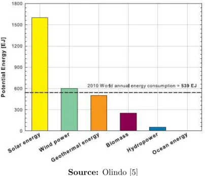
solar energy, have the potential, alone, to meet the total global need for energy. It is also clear in this graph that the potential for the solar energy is, by far, the biggest one.
Figure 2.3: Potential energy production per year of various types of renew-able energy sources.
Source: Olindo [5]
The energy demand is perennially growing. One of the reasons for this growth is the increment in the world’s population. By 2040, there will be nearly 9 billion people on the planet, up from about 7 billion today [6]. In other words, the population will grow by more than 30% over the next 30 years. This growth will not occur uniformly around the globe. Soubbotina [7] claims that most of this growth will take place in developing countries which have increased the consumption of energy in their path to development. As a consequence of this decentralized growth, the energy usage will increase with higher a rate than the rate of population growth. According to U.S. Energy Information Administration (EIA) [8] the energy consumption will increase by 56% by 2040 in reference to 2010. In this scenario, solar energy arises as the better choice to supply the large demand that is coming without increasing the concentration of CO2 in the atmosphere. The overall participation
presents the fastest growing rate among the sources of energy that are not dependent of fossil fuels [9]. Thus, if it keeps the trend of growth, in a few years solar energy will be the most important energy source not based on burning fossil fuels. According to European Photovoltaic Industry Association (EPIA) [9], in 2012 the global solar energy installed power reached the mark of 100 GW. As can be seen in Fig. 2.4, most of this installed power was found in Europe with Germany leading the World with about 31% of the total photovoltaic (PV) installed capacity. Germany, however, is far from presenting the best potential to generate electricity from sunlight.
Figure 2.4: Global photovoltaic cumulative installed capacity share in 2012 (MW; %).
Source: European Photovoltaic Industry Association [9]
Figure 2.5 shows the total irradiance on the horizontal plane in Germany and Brazil. Comparing the irradiances on both countries it is possible to conclude that the worst scenario in Brazil is about 40% better than the best scenario in Germany. Therefore, there is a huge open market for PV in places like Brazil where the potential is enormous but the installed power is still very low.
conventional energy sources from fossil fuels with an average cost of about 83 US$/MWh. It should be mentioned here that current photovoltaic cost estimates are calculated on the price of Si-based solar cell technology which is the current technology on the marketplace. Thus, enormous research efforts are being directed towards the development of new types of solar cell devices characterized by low-cost, high efficiency and stable long lifetimes. The use of semiconductor oxides can be a strategy to reduce the price of photovoltaics.
Figure 2.5: Total irradiance on the horizontal plane on Germany (left) and on Brazil (right).
Source: Salamoni and R¨uther [10]
2.1.2 Solar spectrum
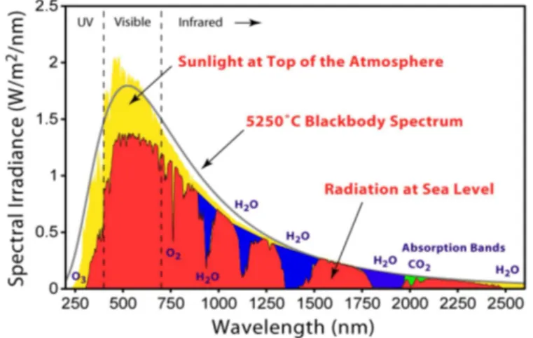
constant. According to Kininguer [11], the value of the solar constant is 1367 W/m2. The
solar spectrum covers energy values from ultraviolet (UV) to infrared (IR) where 45.7% is in the infrared region, 47.3% in the visible range, and 7.0% in the ultraviolet range [3]. Almost all absorbs used in solar cells have the ability to harvest light on the UV and visible ranges with IR photons simply lost. Nevertheless, a great deal of effort has been dedicated to the development of materials or structures that can harvest photons in the IR range [12–14].
Figure 2.6: Solar spectrum at the top of the atmosphere, at sea level, absorption bands and black-body radiation at 5523 K.
Source: Callister Jr and Rethwisch [15]apudAbreu [16]
As can be seen in Fig. 2.6, there are some absorption bands on the spectrum at sea level. The absorption on the spectrum depends on the air mass, AM, defined as:
AM = 1
cosθ (2.1)
Figure 2.7: Solar spectrum at the top of the atmosphere, at sea level, ab-sorption bands and black-body radiation for 5523 K.
Source: Own author
2.1.3 A brief history of the photovoltaic technology
Photois the Greek word for light whilevoltaicis referred to electricity (from Alessandro Volta, Italian Physicist who invented the electric battery). Therefore, the term photo-voltaics is commonly used as the process of transformation of light energy (or solar energy) into electric energy.
The basic science behind the photovoltaic effect was first observed in 1839 by the nineteen-year-old French physicist Alexandre Edmond Becquerel. Becquerel observed a physical phenomenon allowing light-electricity conversion while experimenting with metal electrodes and electrolytes. In 1883 Charles Fritts, an American inventor, described the first solar cells made from selenium wafers. In 1888 Edward Weston receives a first US patent for a ”solar cell”. Therefore, photovoltaics is an ancient technology more than 170 years old [17].
proposed a theoretical explanation for the photoelectric effect [18]. Some years later, in 1916, Robert Millikan provided experimental proof of Einstein’s theory of the photoelectric effect. Due to this success, Einstein received the 1922 Physics Nobel Prize for his work on the photoelectric effect. Approximately three decades later, a Bell laboratories team discovered that silicon had photoelectric properties and quickly developed Si solar cells achieving efficiency of 6%. Early satellites were the primary use for these first solar cells. The commercial solar age had then began. On the next years the advancements concentrated on spacial applications. By the occasion of the 1970’s oil crisis, also referred as oil shock, when the price of the oil quadrupled in less than half a year [11], alternative sources of energy gained a big importance. Research drived PV costs down about 80%, allowing for applications such as offshore navigation warning lights and lighthouse horns, railroad crossings, and remote use where utility-grid connections are too costly.
More recently, global warming and climate change have become issues of evergrowing concern. The use of renewable sources of energy has become even more encouraged. In fact, the rising attention that global warming has increased, has forced the world leaders to embrace some goals in order to minimize this effect. The Kyoto Protocol is an example of how the leaders decided to face the problem. On the Kyoto Protocol the goal was the reduction, by 2012, of at least 5.2% on the emissions of greenhouse gases by developed countries regarding to levels recorded in 1990. Those conditions, together with considerable subsidy programs have provided the means for an extraordinary growth of the photovoltaic industry for a relatively long period of time. Nowadays the photovoltaic industry is one of the fastest growing industries in the world and exist largely without subsidies [11].
2.1.4 Physical principles
photovoltage) [19]. Particularly, this occurs when the energy of the photons making up the light is larger than the forbidden band gap of the semiconductor. However, in normal conditions the excited electrons relax back quickly to their original or ground state. In a photovoltaic device, there is a built-in asymmetry which pulls the excited electrons away before they can relax, and feeds them to an external circuit. The extra energy of the excited electrons generates a potential difference or electron motive force (e.m.f.). This force drives the electrons through a load in the external circuit to do electrical work.
2.1.5 Semiconductors
According to quantum mechanics every atom presents a set of discrete electronic en-ergy levels, which are separated by gaps on the enen-ergy scale. In a typical semiconductor’s crystal structure, atoms are separated by few ˚A allowing interaction between these dis-crete energy levels spreading them into energy bands. The highest energy band containing electrons at 0 K is called the valence band, and the conduction band is defined as the energy band where electrons can conduct net current by moving through the unoccupied energy states.
The gap in energy between the top of the conduction band,EC, and the bottom of the
valence band, EV, is the forbidden energy band gap EG = EC −EV. On the ideal case
no energy states are allowed inside the band gap. Photons with energy greater than or equal to EG may be absorbed by electrons in the valence band, exciting them across the
gap into the conduction band. In some cases, doping impurities and unintentional defects create energy levels in the forbidden band and are responsible for many semiconductor properties that lead to practical applications.
The Fermi level, EF, is defined as the energy level above which there is no occupied
Fermi-Dirac distribution function:
F(E) = 1
1 + exp E−EF
kT
(2.2)
The band structure governs the electronic characteristics of solids. The solids can be classified in terms of its conducting properties as conductors, insulators and semiconduc-tors. In a conductor, the conduction band is partially filled or there is an overlapping between the conduction and valence bands. This kind of material has a zero band gap. Electrons subject to a small applied field are free to move. On the other hand, the band gap in an insulator is so large that essentially no electrons can be excited to the conduction band to contribute to the current flow. Semiconductors present conducting properties in between those of conductors and insulators. A semiconductor possesses a relatively nar-row band gap and, at low temperature, behaves like an insulator. At higher temperature, however, there is a reasonable probability of electron excitation from the valence band to the conduction band, so electrons can contribute to the current in the conduction band. The promotion of an electron to the conduction band leave a hole in the valence band, creating an electron-hole pair. Under the action of an external field the electrons and holes carry current in opposite directions. Hence, the sum of the motion of electrons in the conduction band and holes in the valence band contributes to the current flow in a semiconductor.
2.1.5.1 Properties of semiconductors
One of the most important properties of a semiconductor is that it can be doped with different types and concentrations of impurities to vary its resistivity. Also, when these impurities are ionized and the carriers are depleted, they leave behind a charge density that results in an electric field and sometimes a potential barrier inside the semiconductor. Such properties are absent in a metal or an insulator.
generated carriers. The conduction electron concentration,n, in intrinsic semiconductors in thermal equilibrium at a given temperature without any external excitations such as light or electric field is given by:
n = Z ∞
Ec
N(E)F(E)dE (2.3)
where N(E) is the number of states at the conduction band and F(E) is the occupancy of its states [20]. By means of the Fermi-Dirac integral and Boltzman statistics,n can be written as:
n=NC exp
−EC −EF
kT
(2.4)
where NC is the effective density of states in the conduction band. Similarly, the hole
density, p, in the valence band can be derived:
p=NV exp
−EF −EV
kT
(2.5)
whereNV is the effective density of states in the valence band.
For intrinsic semiconductors, the electron density in the conduction band is equal to the hole density in the valence band:
n=p=ni (2.6)
whereni is the intrinsic carrier density which may be obtained from eqs. 2.4 and 2.5 and
written as:
ni = (NCNV)1/2exp
−EG
2kT
(2.7)
whereEG =EC−EV is the energy band gap.
to the conduction band at moderate temperatures. A semiconductor doped with donor impurities usually has additional negatively charged carriers and thus are called n−type semiconductors.
Similarly, impurities which create states with relatively small ionization energy re-garding to the top of the valence band, are known as acceptors. Electrons can be excited from the valence band to the acceptor states at moderate temperatures leaving a hole in the valence band. Therefore, a semiconductor doped with acceptor impurities usually has additional positively charged carriers and are calledp−type semiconductors.
Electrons are the majority carriers and holes are the minority carriers inn−type semi-conductors while holes are the majority carriers and electrons are the minority carriers inp-type semiconductors. For extrinsic semiconductors, n is generally close to the donor concentration ND in n−type semiconductors whereas p is close to the acceptor
concen-tration NA in p−type semiconductors [21]. Using eqs. 2.4 and 2.5, the Fermi energy of
extrinsic semiconductors is given by:
EF =EC −kTln
NC
ND
(2.8)
forn-type semiconductors, and
EF =EV +kT ln
NV
NA
(2.9)
for p−type semiconductors. With respect to intrinsic semiconductors, the Fermi energy level of an−type semiconductor is closer to the conduction band while that of a p−type semiconductor is closer to the valence band.
As mentioned before, the band gap is the energy difference between the bottom of the conduction band and the top of the valence band. However, the bottom of the conduction band and the top of the valence band are not, in general, at the same point in reciprocal space. If EV and EC are aligned in reciprocal space the band gap is referred to as direct.
Figure 2.8: Energy band structure for Si on the left with indirect transition band gap and GaAs on the right with direct transition.
Source: Sze and Kwok [20]
This difference between direct and indirect band gaps is very important as a photon with energy of the order of a semiconductor band gap carries a very small momentum. In a direct gap semicondutor, a photon of energy EG (or larger) can promote an electron
from the valence to the conduction band (to produce an electron-hole pair) quite easily because the electron does not need to be given very much momentum.
However, to be promoted to the valence band of an indirect gap semiconductor, an electron must undergo a change in momentum that can not be provided by a photon. Therefore, an indirect transition is carried out by a simultaneous absorption, by the electron, of a photon and a phonon where the former provides the required energy and the latter the required momentum.
The carrier lifetime is defined as the average time it takes for carriers to recombine, and the carrier diffusion length is the average distance these carriers travel before they recombine. There are three different recombination mechanisms: (a) Radiative recombination: It is a reverse process of the absorption. It occurs with emitted light and happens more rapidly in direct-band-gap semiconductors; (b) Auger recombination: In this recombina-tion process, the released energy excites another electron to a higher energy level instead of emitting light. This excited electron then thermalizes back down to the conduction band edge. Auger recombination is especially probable in heavily doped material. (c) Recombination through traps: Impurities and defects can form energy levels in the for-bidden band. Therefore, electrons can relax from the conduction band to these energy levels and then recombine with holes in the valence band. This process is particularly likely if the energy levels are near the middle of the band gap.
2.1.5.2 p−n junctions
When an−type semiconductor and a p−type semiconductor are put in contact, they form a p−n junction. If the p−type and the n−type regions are composed by the same material, the junction is called homojunction, while when the materials are different, the junction is called heterojunction. As mentioned before, the Fermi energy of a n−type semiconductor is closer to the conduction band while it is closer to the valence band for ap−type semiconductor.
2.1.5.3 Solar cells operation
A solar cell can be considered as a two terminal device that functions like a diode in the dark and generates a photovoltage when illuminated. Under illumination a solar cell has the ability to convert light energy into electrical energy [21, 22]. The semiconductor diode is fashioned when an n−type and a p−type semiconductor are brought together to form a p−n junction. This is typically achieved through diffusion or implantation of specific impurities (dopants) or via a deposition process. The diode’s other electrical contact is formed by a metallic layer on the back of the solar cell [23]. A simple conventional solar cell structure is depicted in Fig. 2.9. As shown in the figure, the sunlight strikes the solar cell and it delivers electrical energy.
Figure 2.9: Schematic representation of a simple conventional solar cell.
Source: Gray [23]
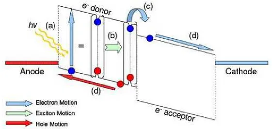
1. a light absorption process which causes a transition in a material (the absorber) from a ground state to an excited state,
2. the conversion of the excited state into (at least) a free negative and a free positive-charge carrier pair, and
3. a discriminating transport mechanism, which causes the resulting free negative-charge carriers to move in one direction (to a contact called the cathode) and the resulting free positive charge carriers to move in another direction (to a contact called the anode). The energetic, photogenerated negative-charge carriers arriving at the cathode result in electrons which travel through an external path (an electric circuit). While traveling this path, they lose their energy doing something useful at an electrical load and finally they return to the anode of the cell. At the anode, every one of the returning electrons completes the fourth step of photovoltaic energy conversion, which is closing the circle by
4. combining with an arriving positive-charge carrier, thereby returning the absorber to the ground state.
2.1.6 Characterization techniques
2.1.6.1 Current densityvs. voltage: J−V curves
A J−V measurement under standard test conditions (AM 1.5 spectrum and 25◦C) provides a fingerprint of a solar cell and it is the most common tool for solar cells char-acterization. The J − V curve of an ideal solar cell follows the ideal diode equation:
J =JS
eqVkT −1
(2.10)
where JS is the saturation current density and V the applied voltage. When light is
J =JS
eqVkT −1
−JL (2.11)
Under realistic conditions, additional parameters need to be considered. Equivalent circuit models define the entire J −V curve of a cell, and it is a good tool to take into account these additional parameters. One basic equivalent circuit model in common use is the single diode model shown in Fig. 2.10.
Figure 2.10: Schematic representation circuit of a photovoltaic cell.
Source: Gray [23]
Using Kirchoff’s current law the current I through the circuit shown in Fig. 2.10 can be written as:
I =IL−ID−Ish (2.12)
where IL is the light-generated current in the cell, ID is the voltage-dependent current
lost to recombination, and Ish is the current lost due to shunt resistances. In this single
diode modelID is modelled using the Shockley equation for an ideal diode:
ID =I0
exp
V +IRs
AVT
−1
(2.13)
ideality factor, andVT is the thermal voltage given by:
VT =
kTc
q (2.14)
where k is Boltzmann’s constant, Tc is the cell’s working temperature and q is the
ele-mentary charge. Usually, A = 1 when ideal diffusion currents dominate, A = 2 when recombination currents dominate, and 1≤A≤2 when both currents are comparable.
Writing the shunt current in terms of Rs and the shunt resistanceRsh as
Ish = (V +IRs)/Rsh (2.15)
and substituting this expression together with eq. 2.13 in eq. 2.12 yields Kirchoff’s current law for the current through the model circuit:
I =IL−I0
exp
V +IRs
AVT
−1
− V +IRs
Rsh
(2.16)
As the current generated by a solar cell depends on its area, the current densityJ, defined asI/area, is more often used than the current itself.
A solar cell is characterized by a number of parameters. The open circuit voltage Voc
is the maximum value of the potential difference and is obtained when the terminals of the cell are isolated with infinite load resistance. The short circuit current density Jsc is
the maximum current that a solar cell can produce and is measured when the terminals are connected to each other with zero load resistance. These parameters can be easily obtained by means of a J−V curve like shown in Fig. 2.11.
The cell power density is given by P = JV. The maximum power density Pmax
determines the cell’s efficiency. It occurs at a certain voltage Vmax corresponding to a
given current densityJmax as shown in Fig. 2.11. The fill factor F F is defined as:
F F = VmaxJmax VocJsc
(2.17)
the maximum output power to the incident light power Ps as:
η = VmaxJmax Ps
= VocJscF F Ps
(2.18)
Typically, the power density of the AM 1.5 spectrum is used and thus:
η= VocJscF F
100 mW/cm2 (2.19)
Figure 2.11: Example of a typicalJ −V curve for a solar cell.
Source: Gonzalez-Valls [25]
zero. A straightforward method of estimating the series resistance from a solar cell is to find the slope of the J−V curve at the open-circuit voltage point.
Moreover, near the open-circuit voltage, the J −V curve is strongly effected by the shunt resistance. Significant power losses caused by the presence of a shunt resistance are typically due to manufacturing defects, rather than poor solar cell design. Low shunt resistance causes power losses in solar cells by providing an alternative current path for the light-generated current. Such a diversion reduces the amount of current flowing through the solar cell junction and reduces the voltage from the solar cell. The effect of a shunt resistance is particularly severe at low light levels, since there will be less light-generated current. The loss of this current to the shunt therefore has a larger impact. In addition, at lower voltages where the effective resistance of the solar cell is high, the impact of a resistance in parallel is large. The effect of the series and shunt resistance in the J−V curve is depicted on Fig. 2.12.
Figure 2.12: Effect of the modification of (a) series resistance and (b) shunt resistance in a solar cellJ−V curves.
Source: Gonzalez-Valls [25]
2.1.6.2 External quantum efficiency
inci-dent photons at a specified wavelength. IPCE is a product of light harvesting, injection and collection efficiencies. The spectral response is obtained through electrical measure-ments for a device under illumination in different wavelengths in open circuit condition. Under these circumstances the IPCE can be defined as the ratio between the photocur-rent and the intensity of monochromatic incident light. Reflection and absorption on the superstrate, the TCO (transparent conductive oxide) layer, as well as the incomplete absorption of photons can contribute to the losses in external quantum efficiency.
The number of charges generated in the device per unit time and unit area is given by:
Nc =
Jsc
q (2.20)
and the number of incident photons per unit time and unit area is given by:
Nf =
Iλ
hc/λ (2.21)
were Iλ is the intensity of the source, h is the Planck constant, c the speed of light in
vacuum andλthe wavelength of the incident radiation. The EQE can then be written as (plugging in the values of constants):
EQE = Nc Nf
= 1240× Jsc
Iλλ
(2.22)
If the EQE is obtained under true Jsc conditions (AM1.5 illumination, V = 0), then it
can be related to the photovoltaic parameter Jsc
Jsc =q
Z
ΦAM1.5 EQE(λ) dλ (2.23)
where ΦAM1.5is the photon flux of AM1.5 illumination. It is usually impractical to perform
EQE measurements under true Jsc conditions, and fortunately eq. 2.23 generally holds
2.1.7 Thin Film Photovoltaics
Thin film photovoltaics encompasses those called “excitonic solar cells” such as DSSCs (dye sensitized solar cells), OPVs (organic photovoltaics) ss-DSSCs (solid state dye sen-sitized solar cells). Excitonic solar cells (XSCs) consist of solar cells in which light ab-sorption results on the production of a transiently localized excited state, called exciton, that cannot be thermally dissociated (binding energy ≫ kT) in the chemical phase in which it was formed. Examples of XSC include molecular semiconductor solar cells, con-ducting polymer solar cells, dye-sensitized solar cells, quantum dot solar cells. These thin film photovoltaics (TFPV) devices also encompass a new type of solar cell called hybrid perovskite solar cell.
Currently, there are four generations of solar cells: silicon, inorganic, excitonic, and Perovskite solar cells [1, 25].
The first generation of solar cells refers to a singlep−njunction of crystalline Si (c-Si), exhibiting up to 25% conversion efficiency (laboratory scale). This efficiency approaches the theoretical energy conversion efficiency limit of 31%, which is known as the Shockley and Queisser (S-Q) limit. These silicon-based solar cells currently have the highest effi-ciency, which is being rapidly challenged by perovskite solar cells, but they are also the most expensive.
Second generation solar cells include inorganic thin films: amorphous silicon (a-Si), cadmium telluride (CdTe), or copper (gallium) indium selenide/sulphide. These solar cells are less expensive than conventional silicon solar cells, and they can be fabricated as flexible devices. Nevertheless, their lower efficiency compared to silicon solar cells and the use of toxic metals are important issues hindering commercialization.
limit. Because XSCs are less expensive than second generation solar cells, third generation solar cells are considered the most suitable solar cells for flexible and printable devices. However, their low efficiency and challenges with stability are significant issues preventing their entrance into the market.
Fourth generation solar cells are known as perovskite solar cells. Metal-organic per-ovskites could be the “missing link” between inorganic and organic semiconductors [26]. In only five years of development, hybrid perovskite solar cells have attained power con-version efficiencies that took decades to achieve with the top-performing conventional solar cell materials. Despite the incredible improvement in the photovoltaic performance of perovskite solar cells, critical questions must be answered such as: are the devices excitonic? If so, what is the exciton diffusion length? What are the carrier lifetime and recombination dynamics? Recently, Zhang et al. [27] have demonstrated that the spin configuration affects the rate at which electron-hole pairs split apart or recombine in per-ovskite solar cells, suggesting that these devices are not excitonic. Moreover, the generally low stability ascribed to perovskite solar cells is a significant obstacle for the commercial viability of metal-halide perovskite solar cells. However, a recent study has reported more than 2000 hours of stability for these devices [28].
In addition to the four well-known generations of solar cells, other types of solar cells exist that do not easily fit in any of these categories, such as kesterite solar cells and all-oxide solar cells. Kesterite solar cells are thin film solar cells, which differ from second generation solar cells because kesterite solar cells are only composed of abundant, non-toxic elements. In fact, the kesterite crystal structure represents a group of compound semiconductors such as Cu2ZnSnS4 (CZTS) and Cu2ZnSnSe4 (CZTSe). In fact, CZTS
semiconductors, i.e., CdTe, copper indium selenide (CIS), or CIGS, are used as absorbing layers. In all-oxide solar cells, the metal oxides are also used as absorbing layers. This class of devices have recently attracted considerable attention due to their promising potential for reducing solar cell costs through inexpensive materials and production methods [31]. Heterojunction ZnO/Cu2O cells are the most efficient system investigated so far, reaching
efficiencies of almost 5% [32].
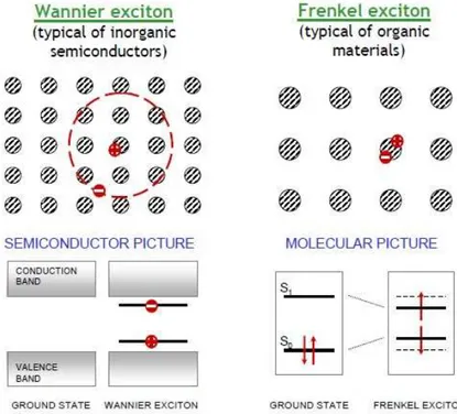
2.1.7.1 Excitons
An exciton is a quantum of electronic excitation energy travelling in the periodic structure of a crystal; it is electrically neutral and hence its movement through the crystal gives rise to the transportation of energy but not charge [33]. The neutrality of this quasiparticle comes from the fact that an exciton can also be described as a bound state of an electron and an electron hole. The electrical charge from the electron and electrical hole cancels each other. This electron-hole pair is kept bound due to Coulombic electrostatic attraction. The exciton can be treated as a particle, it moves, present spin and have a strong bind energy [34].
Excitons mediate the absorption and emission of light, particularly in disordered and low-dimensional materials. To understand the work principles of solar cells it is necessary the understanding of this excitation. Excitons behave slightly different in organic or inorganic semiconductors. In inorganic semiconductors they are easily separated into free electron-hole pairs, which does not happen in organic semiconductors. The reason for that is that the dielectric constant ǫfor inorganic semiconductors is relatively large compared to that of organic semiconductors. Figure 2.13 illustrates these two kinds of excitons on inorganic and organic semiconductors.