Article
Printed in Brazil - ©2011 Sociedade Brasileira de Química0103 - 5053 $6.00+0.00
A
*e-mail: [email protected]
Study of Growth, Optical and Morphological Properties of Zn(O;OH)S Thin Films
Synthesized by CBD Method
W. Vallejo,*,a E. Romeroa and G. Gordillob
aDepartamento de Química and bDepartamento de Física,
Universidad Nacional de Colombia, Bogotá, AA14490, Colombia
Neste trabalho, investigamos Zn(O;OH)S como substituto para ao CdS, que é convencionalmente usado como camada tamponante em células solares usando calcopirita. Filmes finos de Zn(O;OH)S foram depositados em banho químico de deposição (CDB), método que utiliza um banho químico contendo tiouréia, acetato de zinco, citrato de sódio e amônio. Filmes finos de CuGaSe2 (CGS) e vidro
soda-cal foram utilizados como substratos. A equação de Avrami foi utilizada para estudar a taxa de crescimento de uma fina película de Zn(O;OH)S sobre ambos os substratos. A influência do tipo de subtrato, do tempo de síntese sobre a taxa de crescimento, as propriedades ópticas e morfológicas dos filmes finos crescidos como Zn(O;OH)S foram avaliadas com espectrofotometria e técnicas de microscopia de força atômica (AFM). Condições adequadas foram encontradas para síntese de filmes finos de Zn(O;OH)S para serem usadas como camadas tampão em celulas solares de CGS.
In this work, we investigated thin films of Zn(O;OH)S as substitute of thin films of CdS, which are conventionally used as buffer layer in chalcopyrite based solar cells. Thin films of Zn(O;OH)S were deposited by chemical bath deposition (CBD) method using a chemical bath containing thiourea, zinc acetate, sodium citrate and ammonium. Soda-lime glass and soda-lime glass covered with thin
films of CuGaSe2 (CGS) were used as substrates in the deposition of thin films of Zn(O;OH)S.
The Avrami equation was used to study the growth rate of thin film of Zn(O,OH)S on both substrates. The influence of the substrate kind and time of synthesis on the growth rate, optical and morphological properties of the as-grown thin films of Zn(O,OH)S have been carried out through spectrophotometry and atomic force microscopy (AFM) techniques. Finally, we found suitable conditions for synthesis of thin films Zn(O,OH)S to be used as buffer layer in CGS based solar cells.
Keywords: solar cells, buffer layer, Zn(O,OH)S, CBD
Introduction
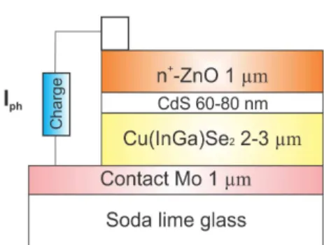
Nowadays, the standard device structure of Cu(In,Ga)Se2 (CIGS)-based solar cells includes a very thin film of CdS (ca. 50 nm) synthesized by chemical bath deposition (CBD) method. This layer works as buffer layer between the CIGS absorber layer and the transparent conductor oxide (TCO), ZnO is currently used as TCO. A typical CIGS-based solar cell structure is shown in Figure 1. The buffer layer is very important to obtain a correct performance of the solar cell, since this layer decreases the mechanical tension stress between absorbent layer and TCO electrode. At present, the best results in electrical conversion have been achieved with solar cells fabricated using the structure Mo/CIGS/ CdS/ZnO. The maximum efficiency reported for this type
of devices is 20.1%.1 In the last decade, serious efforts to
in the blue wavelength region by using a material with a wider band gap (Eg) compared to CdS. At present, to obtain
Cd-free buffer layers able to achieve high efficiencies without deteriorate the stability of the solar cell is one of the main topics of research in the area of photovoltaic technology. Different materials such as In2S3, In2Se3 and ZnSe deposited
by different methods have demonstrated good results as alternatives buffer layers in CIGS-based solar cells,2,3
and buffer layers of Zn(O,OH)S prepared by CBD have already demonstrated their potential as alternative buffer material. Efficiencies up to 18.6% have been obtained using Zn(O,OH)S/ZnO as window layer in CIGS based cells.4
In this work, we have deposited good quality Zn(O,OH)S thin films by the CBD method on two different substrates, and the Avrami-Erofeev equation was used to study growth rate of Zn(O,OH)S thin film on different substrate.
Experimental
Zn(O,OH)S thin films were synthesized by CBD method. The Zn(O,OH)S thin films were deposited using a solution containing thiourea (Scharlau) (TU) and zinc acetate (Merck) (ZnAc) as sources of S2− and Zn2+,
respectively; ammonia (99.9% Merck) (NH3) and sodium
citrate (Riedel-de Haën) (Cit) were used as complexing agents of the Zn2+. Soda lime glass (SL) and CuGaSe
2 (CGS)
deposited on soda lime glass were used as substrates. The reagent concentrations were ZnAc (0.015-0.120 mol L-1),
TU (0.075-0.500 mol L-1), Cit (0.015-0.045 mol L-1) and
NH3 (0.150-0.600 mol L-1). The bath temperature was
between 50 and 80 °C and the solution pH between 10 and 11.5. The entire reaction can be written as follows:5
[Zn(NH3)4-xHCitx](ac) + NH2SCNH2(ac) + OH
−
[Zn(O,OH)S]film + HCit + NH3 + NCNH2 + H2O (1)
The film thickness was measured using a Veeco Dektak 150 profilometer. The surface morphology of as-grown Zn(O,OH)S thin films was studied using a microscope from Park Scientific Instruments (PSI), an atomic force microscopy (AFM) with a scanned area (2 µm × 2 µm) using non-contact mode. Finally, the optical analysis was done spectrophotometrically through Ocean Optics HR2000CG UV-NIR in the range of 300-1000 nm.
Results and Discussion
Thin films growth
The variation of the thickness of Zn(O,OH)S thin films as a function of time and substrate type is plotted in Figure 2. It is observed that the growth rate of the Zn(O,OH)S films is significantly affected by time and substrate type. Two different regions can be distinguished during the growth process of Zn(O,OH)S thin films (see Figure 2a): an initial linear region (between 20 and 50 min) and the final saturation region (after 150 min), which are typical of CBD processes. Before starting the linear growth region,
there is a period of time (called induction time), during which the nucleation process is induced, this is an important step being necessary to begin the film growth. During the stage of linear growth, the film thickness increases linearly with time. Finally, during the saturation stage, the growth rate decreases significantly as consequence of a reduction of the reagent concentrations in the solution. Figure 2a shows Zn(O,OH)S thin films grown on the two different substrates (SL and CGS). It is observed that the substrate type significantly affects the growth rate. The results also show that the Zn(O,OH)S thin films grew faster on CGS than on SL. This behavior could be explained taking into account that the CBD growth process is affected by the surface kinetic processes.6 The behavior observed in the
zone of linear growth (Figure 2a), where the thickness of the film changes linearly with time, suggests that this stage of the process can be controlled by the number active sites in the substrate surface.7 The number of possible sites
available for the formation of nuclei can be determined by the composition and morphology of substrate. In general the presence of defects as vacancies and interstitials (Cu, Ga, Se) commonly found in this type of compound can facilitate the presence of those sites. Furthermore, the surface roughness affects the films adhesion and growth due to the greater contact surface area per geometric surface area and the possibility of anchoring of the initial deposit in pores of the substrate.
The formation of the thin film is based on the nucleus generation and succeeding growth, when the whole reaction occurs under constant temperature, the Avrami-Erofeev equation can be used to approximate some of the kinetic parameters of the reaction. This is an expression of formation rate of the nuclei in the special case when there is completely random nucleation.7 This kind of general
model is attractive for CBD processes. The formal kinetic expression such as the Avrami-Erofeev equation:8
α = 1 – e–ktn (2)
where α is the fractional decomposition, t the time, k is a
rate constant and n the Avrami exponent which determines the nucleation and growth mode. Equation 2 can be written as:
ln [–ln (1 – α)] = ln k + n ln (t) (3)
Plotting ln[−ln(1 −α)] vs. ln(t) the reaction constant (k)
and the Avrami exponent (n)can be obtained from the slope and the intercept of the lineal fitting. In Figure 2b, ln [−ln (1 −α)] vs. ln (t) curve is showed and, in Table 1,
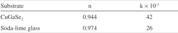
the kinetic parameters are listed. Table 1 shows that n
values are approximately the same and this indicates that both types of substrate could present the same crystal nucleation mechanisms. It is known that the n value is related with dimension particle growth, in our case the n values are close to one, indicating that the growth occurs in one dimension, probably like a columnar growth. The addition of material from chemical solution to the film in formation could follow this mechanism. On the other side, unlike n the k value changes significantly on substrate type; the value of k duplicates when CGS absorbent layer is used. This corroborates that the growth process occurs faster on CGS than SL and give a quantitative tool to compare the growth rate on both substrates.
Due to the fact that n presents a similar value in both substrates, the nucleation way could be the same and probably follows a columnar growth. Then the CGS substrate must present a greater number of active sites for generation of nuclei than SL substrate for growth of Zn(O,OH)S crystals. It occurs as a a result of the differences in composition and topography of the surface.
Optical characterization
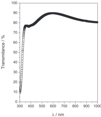
The optical properties of thin film of Zn(O;OH)S were determined from transmission measurements in the range of 300-1000 nm. Figure 3 shows the transmission spectrum of thin film of Zn(O;OH)S (around 150nm). Figure 3 corresponds to the forbidden electronic transition for materials with a direct transition. In this case the electronic transition between valence and conduction band does not involve a change in electronic momentum (k), and thus the absolute minimum of the conduction band and the absolute maximum of the valence band occur at the same point in the k-space. Figure 3 shows an optical transmission about 75-85% in the visible range. This high transparency in the visible region indicates that there are not colloid particles formed by homogeneous reaction on the surface substrate. Furthermore, a sharp absorption edge is observed in the visible region, indicating the good crystallinity and a low defect density near to the band edge.9 This result is very important because the material
obtained in this work presents a high transmittance in the visible region fulfilling one of the most important requirement for a buffer layer.
Table 1. Growth kinetic parameters of Zn(O,OH)S thin films synthesized on different substrate types by CBD
Substrate n k × 10-3
CuGaSe2 0.944 42
The measured spectral dependence of transmittance was converted to spectral dependence of the absorption coefficient, using equation 4:
(4)
where α is the absorption coefficient, d is the film thickness
(obtained by profilometry). The optical energy band gap of the films was determined using the relation:
(αhν)2 = A(hν – E
g) (5)
where Eg is the band gap energy and A is a constant
depending on the transition probability. The optical band gap of the films was determined by extrapolating the linear portion of the (α hν)2vs. hν plot on the x-axis.10
Figure 4 shows the (α hν)2 vs. hν for thin films of
Zn(O;OH)S. It is observed that band gap from thin film of Zn(O,OH),S (3.78 eV) was greater than band gap of bulk ZnS (3.65eV).11-13 Two reasons can explain these results:
(i) the quantum effect and (ii) chemical composition of the film. The thin films of Zn(O;OH)S have shown the presence of nanocrystalline particles. Additionally, it is known that the co-precipitation of others species in CBD process is common. In the formation of thin films of Zn(O;OH)S, the precipitation of Zn(OH)2 and ZnO can be present. These
compounds can shift the band gap to blue energies like in this case. Thus, the co-precipitation could be the reason for the shift of the band gap to blue energies. This blue
change is very favorable because of the blue response of solar cells is improved.
These results suggest that Zn(O;OH)S thin films have adequate optical properties to be use as buffer layer to replace the CdS because Zn(O;OH)S thin films have bigger bad gap than CdS (2.4 eV)14 and present high transmittance. This
results suggest that solar cells response to blue energies could be improve using Zn(O;OH)S thin films as buffer layers.
Morphological characterization
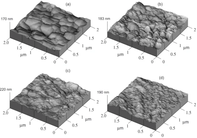
Figure 5 shows AFM images of Zn(O,OH)S thin films deposited by CBD on CGS substrates as function of time. In Table 2 are listed the corresponding grain size average and roughness (Rms) values, which were determined analyzing
the AFM images showed in Figure 4, through the ProScan image analysis software. Figure 5a shows the CGS-substrate AFM image, in this figure is observed columnar crystals, typical for CGS with a tetragonal structure. Figure 5 also shows the Zn(O,OH)S thin film thickness effects on morphology. It is clearly seen from the AFM images that the grain size of Zn(O,OH)S particles are smaller than grain size of CGS particles (220 nm). Additionally, at 40 min of process, different sized grain particles are distributed randomly throughout the substrate without any crack (Figure 5) and it is seen that Zn(O,OH)S thin films grain size and Rms roughness increase significantly when
the film thickness increases (Table 2). At the initial stage of deposition, many nucleation centers are present on the Figure 3. Optical transmission spectrum of as-deposited Zn(O,OH)S thin
films with 90 nm thickness.
Table 2. Grain size average and roughness (Rms) values derived from
images displayed in Figure 5
Sample Grain size / nm Rms / nm
CuGaSe2/Zn(O,OH)S20min 44 1.5
CuGaSe2/Zn(O,OH)S40min 82 2.0
CuGaSe2/Zn(O,OH)S60min 110 2.7
Figure 5. Atomic force micrographs of as-deposited Zn(O,OH)S thin films deposited on AgInS2 with different synthesis times: (a) 0, (b) 20, (c) 40 and (d) 60 min.
substrate and smaller crystallites are produced. For shorter time deposition intervals, the films with smaller crystallites are not able to grow into bigger ones, whereas for thicker films the crystallites can be bigger. Finally, Figure 5 clearly shows that after 60 min of CBD process is possible to cover completely and uniformly the CGS surface.
Conclusions
Experimental conditions for synthesis of thin films of Zn(O,OH)S through CBD method were obtained in this work. The Zn(O,OH)S buffer layers deposited under CGS substrates were uniform, adherent and presented high transmittance in the visible region of the electromagnetic spectrum. The Avrami-Erofeev equation was used to fit the
growth curves. This model indicated that the nucleation process could be the same on the both surfaces used as substrates. The growth process was faster on CGS than SL due to the differences in surface composition and morphology of the substrates. The optical characterization indicated that Zn(O,OH)S layers present bigger bang gap than CdS, the conventionally used as buffer layer. Finally, the thin films of Zn(O,OH)S obtained in this work can be used as buffer layer to replace the toxic CdS buffer layer in solar cells based on CGS.
Acknowledgements
This work was supported by Colciencias and DIB-Universidad Nacional de Colombia
References
1 Green, M. A.; Emery, K.; Hishikawa, Y. M; Warta, W.; Prog. Photovolt.: Res. Appl.2010, 18, 346.
2 Vallejo, W.; Clavijo, J.; Gordillo, G.; J. Braz. Phys. 2010, 40, 30. 3 Hariskos, D.; Spiering, S.; Powalla, M.; Thin Solid Films2005,
4 Contreras, M. A.; Nakada, T.; Hongo, M.; Pudov, O. A.; Sites, J. R.; 3rd World Conference on Phorovoltaics Energy
Conversion, Osaka, Japan, 2003, p.570. Document can be
obtained under request to authors.
5 Vallejo, W.; Hurtado, M.; Gordillo, G.; Electrochim. Acta2010,
55, 5610.
6 Froment, M.; Lincot,D.; Electrochim. Acta1995, 40, 1293. 7 O’Brien, P.; McAleese. J.; J. Mater. Chem. 1998, 8, 2309. 8 Zhai, R.; Wang, R.; Wang, H.; Zhu, M.; Yan, H.; J. Phys. D:
Appl. Phys. 2007, 40, 4039.
9 Cheng, J.; Fan, D. B.; Wang, H.; Liu, B. W.; Zhang, Y. C.; Yan, H.; Semicond. Sci. Techol. 2003, 18, 676.
10 Revathi, N.; Prathap, P.; Ramakrishna Reddy, K. T.; Appl. Surf. Sci.2008, 254, 5291.
11 Roy, P.; Ota, J. R.; Srivastava S. K.; Thin Solid Films2006, 515, 1912.
12 Gao, X. D.; Li, X. M.; Yu, W. D.; Thin Solid Films2004, 468, 43.
13 Naghavi, N.; Henriquez, R.; Laptev, V.; Lincot, D.; Appl. Surf. Sci.2004, 222, 65.
14 Goudarzi, A.; Aval, G. M.; Sahraei, R.; Ahmadpoor, H.; Thin Solid Films2008, 516, 4953.
Submitted: March 31, 2011
![Figure 2. (a) Growth rate variation on time synthesis and substrate type and (b) ln [−ln (1 − α)] vs](https://thumb-eu.123doks.com/thumbv2/123dok_br/18994756.461843/2.892.139.779.690.1080/figure-growth-rate-variation-time-synthesis-substrate-type.webp)