Resonant Energy Transfer in Si Nanocrystal Solids
Rens Limpens,
*
,†Arnon Lesage,
†Peter Stallinga,
‡Alexander N. Poddubny,
§Minoru Fujii,
∥and Tom Gregorkiewicz
††Institute of Physics, University of Amsterdam, Science Park 904, 1098 XH Amsterdam, The Netherlands
‡Center for Electronics, Optoelectronics and Telecommunications, University of the Algarve, 8005-139 Faro, Portugal §Ioffe Physico-Technical Institute RAS, 194021 Saint-Petersburg, Russia
∥Department of Electrical and Electronic Engineering, Graduate School of Engineering, Kobe University, Rokkodai, Nada, Kobe
657-8501, Japan
*
S Supporting InformationABSTRACT: Energy exchange between closely packed semiconductor quantum dots allows for long-range transfer of electronic energy and enables new functionalities of nanostructured materials with a huge application potential in photonics, optoelectronics, and photovoltaics. This is illustrated by impressive advances of quantum-dot solids based on nanocrystals (NCs) of direct bandgap materials, where this effect has been firmly established. Regretfully, the (resonant) energy transfer in close-packed ensembles of NCs remains elusive for siliconthe main material for electronic and photovoltaic industries. This is the subject of the present study in which we conclusively demonstrate this process taking place in dense dispersions of Si NCs in an SiO2matrix. Using samples with different NC configurations, we can directly
determine the wavelength dependent energy transfer rate and show that it (i) can be modulated by material parameters, and (ii) decreases with the NCs size, and thus being consistent with the energyflow proceeding from smaller
to larger NCs. This result opens the way to new applications of Si NCs, requiring energy transport and extraction. In particular, it forms a fundamental step toward development of an excitonic all-Si solar cell, operating in some analogy to polymer devices.
■
INTRODUCTIONNext to the external bias-driven tunneling of carriers,1−4energy transfer (ET) between neighboring NCs based on the intrinsic electronic properties, often described in terms of the Förster mechanism,5constitutes a necessary step for realization of the long-range energy transfer in an ensemble of closely packed NCs. In direct bandgap NCs, ET has been investigated in detail and conclusively demonstrated.6−9 In that research, two NC ensembles, with well-defined but distinctly different average sizes, have been prepared and optically characterized, and then mixed to form a densely packed quantum solid. It was found that upon mixing, the photoluminescence (PL) lifetime of the small NCs was shortened, whereas that of large NCs was extended. Taken together with an efficiency change of the respective PL bands, this result provided an unequivocal evidence of the energy transfer taking place from small to large NCs. Unfortunately, this successful strategy is not available for Si, where development of NCs with a sufficiently narrow size distribution is (still) not achieved. Moreover, theoretical evaluation based on a phonon-less tight-binding approach,10 predicted ET to be inefficient for Si NCs due to the indirect bandgap. Nevertheless, based on experimentalfindings, several reports postulated that ET does take place between proximal Si NCs.11−15 These findings included (i) stretched exponential character of (ensemble) PL decay,11,12,14 (ii) red-shift of PL
spectra upon delay time,12,14and (iii) size-dependent internal quantum efficiencies (IQEs).13,15 However, for all these observations also alternative explanations, not involving ET, could be given: The stretched-exponential character of PL decay can be explained by dispersion of lifetimes of NCs emitting at the same wavelength, which might easily appear, e.g., due to differences in surface passivation/termination or shape.16,17 Similarly, the red shift of PL spectra during decay will also appear as a consequence of lifetime shortening in small “blue” NCs due to enhanced confinement. Lastly, the size-dependent IQE of Si NCs, which increases for larger diameters, can equally well be explained by the generally better crystalline and surface qualities (lower curvature) of larger NCs.18 Ther-Therefore, while these experimentalfindings are consistent with the energy transfer within an ensemble of Si NCs, they do not provide a proof of its occurrence. The goal of this study is to conclusively resolve the important issue of ET between Si NCs. On the basis of the excitation intensity dependent time-resolved emission spectroscopy, we are able to demonstrate and directly quantify ET for an individual sample, enabling us to compare ET rates for Si NCs in different configurations.
Received: July 2, 2015 Revised: July 24, 2015 Published: July 27, 2015
Article pubs.acs.org/JPCC
copying and redistribution of the article or any adaptations for non-commercial purposes.
Downloaded via UNIV DO ALGARVE 00200 on May 4, 2019 at 11:01:57 (UTC).
For the purpose of this study, samples of closely packed Si NCs have been produced. The investigated structures are prepared by magnetron cosputtering, followed by a 30 min anneal in nitrogen atmosphere at 1250°C. This method is well-known to yield high-quality Si NCs with relatively narrow (log-normal) size distributions with dispersions of below 20%. Two kinds of samples have been made, featuring two- and three-dimensional (2D and 3D) NC packing structures (arrays), as schematically illustrated inFigure 1(a)for more details, see
theExperimental Section. In the past, Halivni et al.19showed that resonant energy transfer is influenced by the dimension-ality of the process, and this we could expect in our structures as well. Due to the relatively large separation between 2D sheets of NCs, we expect no energy transfer between NC layerssee also the derivation of the average NC separation later on. As a result, reduction of the energy transfer rate (ΓET) should be observedschematically illustrated as 2D ET confinement in Figure 1(a).
Figures 1(b) and 2(a) display transmission electron microscopy (TEM) and high-resolution TEM (HRTEM) images, respectively, of both structures. By TEM, the superlattice structure of the 2D arrays is confirmed, whereas a random positioning of Si NCs is observed for the 3D array. By HRTEM, the diamond structure of the Si NCs is conclusively established. In order to obtain sufficient statistics for the size determination, more than 100 NCs per sample have been analyzed; the resulting histograms are shown in Figure 2(b). We conclude on the smaller average size and also a narrower size distribution for the NCs in the 2D array when compared to the 3D packing. Having estimated the size distribution, we can calculate the average nearest-neighbor
surface-to-surface distance, RNN, for both structures. By
performing Monte Carlo simulations, we get an RNN of 3.9
and 2.2 nm for the 2D and 3D structures, respectivelysee
Supporting Information(SI) for details. While the exact value of the RNN is sensitive to methodology, the trend is firmly
established, and the 2D structure indeed experiences a larger RNN, intuitively justified by the presence of the passive layer.
We note that, while the dipole−dipole driven ET does not involve photons and therefore is insensitive to the local density of states,20 the ΓET should be strongly influenced by RNN.
Hence, both argumentsdifferences in size distributions and RNN values (based on HRTEM data)strengthen the
hypothesis that ET between Si NCs should be suppressed in the 2D structure.
After this microscopic characterization, spectral and temporal characteristics of PL of the structures could be investigated.
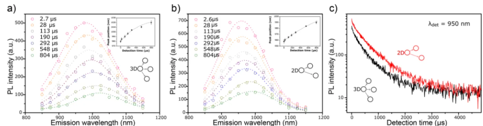
Figure 3(a) and (b) presents time-resolved PL spectra for 3D and 2D NC packing, respectively. We observe for both samples a gradual red shift of the maximum of the PL spectrum upon decayfor clarity, the shifts of PL maxima are explicitly given in the insets. Temporal analysis reveals, for both configurations, PL decay times in theμs-regime, typical for high-quality Si NCs of these sizes prepared by cosputtering. In order tofit the PL transients depicted in Figure 3(c), the stretched exponential function (e−(t/τ)β) was used21(where τ is the lifetime and β is the dispersion factor), with β values between 0.7 and 0.9, as commonly observed.11As previously mentioned, both of these featuresthe temporal red shifting and the stretched exponential decay of PLhave been observed before and misinterpreted asproof of energy transfer within the ensemble of Si NCs.
In order to explicitly probe ET, we make use of PL quenching, which appears when energy is transferred to an already excited NCseeFigure 4(a). In that case, nonradiative recombination of the transferred exciton arises due to an efficient Auger interaction between multiple excitons localized within the same NC. Auger interactions in Si NCs have been investigated in the past22−24 and found to occur on a subnanosecond time-scale, which is beyond the resolution of the current experiment. In fact, the time-resolution of the Figure 1.Structural concept and realization. (a) Schematic illustration
of the 3D and 2D structures on the left and the right, respectively. In contrast to the 3D structure, energy transfer in the 2D arrays is expected to occur only within the individual layers and not between the layers, as schematically indicated. The visualizations are based on the, experimentally determined, NC size and size distributions. (b) Bright-field cross-section TEM images of 3D and 2D array(s) on the left and right, respectively. The random NC distribution and size distribution are clearly visible for the 3D structure, compared to the ordered layer structure for the 2D case.
Figure 2. Structural characterization. (a) HRTEM image and an enhanced (bandpassfilter) version of the same image (below). The crystalline nature of the cluster of Si atoms is deduced from the lattice fringes corresponding to {111} planes of crystalline Si. (b) NC size distributions obtained from analysis of HRTEM images. The histograms are based on analysis of over 100 NCs per sample, with log-normal distribution fit (dashed). The 2D arrays of NCs have a smaller mean size and a narrower size distribution compared to the 3D array.
experiment prohibits the detection of PL transients appearing due to any ultrafast nonlinear effect, whether it is the detection of Auger interactions or, for example, carrier multiplication. Nevertheless, ET toward an excited NC would lead to immediate excitation loss (due to Auger interactions), causing PL intensity loss on the time-scale of ET. Since the number of initially excited NCs will increase with the excitation photon flux, ET will introduce a very characteristic, additional nonradiative recombination path whose rate will increase with the excitation power. In saturation, when all NCs are excited, a single ET event results in exciton quenching and in that way the ET rate in the investigated material (ΓET), can be directly
measured. However, if ET would not occur, as frequently suggested in the past, the effective PL decay time should be independent of the pump power. Figure 4(b) schematically illustrates the idea of the experiment: the presence of ET between NCs manifests itself as a gradual decrease of the effective PL lifetime as the pump laser power is increased to the point where all NCs are excited, i.e., the PL saturation is reached. At this point, an equilibrium situation is obtained between the excitation and de-excitation rates, the latter
comprising the radiative recombination and the nonradiative quenching by energy transfer to the nearest neighbor. Further increase of the excitation power results in the generation of multiple excitons per NC, which leads to their immediate quenching by Auger interaction, and therefore not altering the PL lifetime.
It is important to note that upon increase of the excitation power, besides an ET-induced effect, a lifetime change will also appear due to earlier saturation of PL from larger NCs.25This originates from the fact that while PL is detected within a narrow slit-determined wavelength range (around 1 nm), this line width has to be convoluted with the broad emission (120 meV at 300 K) of a single NC of a particular size.26,27However, when taking into account the size dependent absorption cross sections28 in combination with the expected variation of NC sizes within our narrow wavelength range, the change of effective lifetime, as a result of the saturation effect, remains within the experimental accuracy of the lifetime determination (see theSIfor a detailed evaluation). Therefore, we are able to determine the absolute value of wavelength-dependent ΓET
Figure 3.Optical characterization. In (a) and (b) PL spectra at different delay times are shown. An excitation wavelength of 415 nm is used (see
Experimental Sectionfor the details). Both the 3D (a) and 2D (b) systems show significant red-shift with time, often explained by directional energy flow toward larger NCs. The spectra are produced by plotting the amplitude of the time-resolved transient at different detection wavelengths, for different time delays (from 2.6 to 804 μs). The inset quantifies the red-shift (the black dotted lines function as a guide to the eye). (c) PL transients for both samples measured at a detection wavelength of 950 nm. The stretched exponential character of both transients is clearly visible on the logarithmic-linear plot.
Figure 4.Scheme of the experiment. (a) The concept: we make use of transfer activated luminescence quenching, where transferred energy is quenched if the receiving NC is already excited. This is the result of efficient Auger interactions which induce the nonradiative recombination (NR) of transferred energy on time-scales not detectable within the resolution of the experimental setup. By increasing the excitation power, the probability of ET toward an already excited NC increases and NR take over, shortening the PL lifetime (shown in panel b). (b) Scheme of the expected behavior of the PL decay time versus the excitationfluence for two different scenarios: the absence of ET between the Si NCs (black) and the existence of ET (red).
based solely on the measurements on a single sample, after which it is possible to compare the values, for different samples.
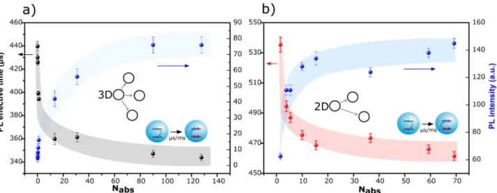
Figures 5(a) and (b) show the experimental results for 3D and 2D packing structures, for an emission wavelength of 950 nm (corresponding to a NC diameter of around 5 nm)the data of other emission wavelengths are depicted in theSI. Since we are interested in probabilities of exciting neighboring NCs, we expresson the x-axisthe excitation power as the average number of absorbed photons per NC (Nabs). In this way, we
end up with a fair comparison of the excitation regime for 2D and 3D samples. Saturation of PL intensity25is used to deduce the properNabsregimeseeSIfor details. We point out on the
rather high Nabs values, which are a result of the strong
attenuation of the excitation beam throughout the sample, hereby causing a big excitation-regime difference between the front and the back surface of the samples. We clearly see that, for both materials, the PL decay time decreases with excitation power, reaching a stable value as PL intensity saturates, i.e., when all the NCs in the ensemble have been excited. The increase of PL intensity is accompanied by a shortening of the effective PL decay time, which approaches a constant value as PL saturation is reached. We note that the concurrent change of the lifetime and PL intensity clearly links the lifetime shortening to excitation of NCs, ruling out other possible explanations of the effect in terms of, e.g., energy transfer to defect states. Therefore, the present result provides direct evidence for the presence of ET between neighboring NCs.
With the experimental results depicted in Figure 5(a) and (b), we can evaluate the transfer rate (ΓET) by subtracting the radiative recombination rate (Γrad) from the experimentally
measured effective recombination rate (Γeff)a reasonable estimation based on the fact that other nonradiative recombination paths, such as defect states, quench PL on a submicrosecond time-scale and are therefore not probed in our experimental setup. The relevantΓrad is calculated using data
from ref 13 corrected for the host parameters of our materialssee SI for details of the calculation procedure. The results are depicted inFigure 6. In the saturation regime, this nonradiative contribution represents the rate of a single ET event, and in that way, we can determine the characteristic ET time constant, for the 3D and 2D NC structures as 0.9 and 3.3
ms, respectively. Hence, in line with the previously discussed expectation, we conclude that theΓETis indeed reduced for the
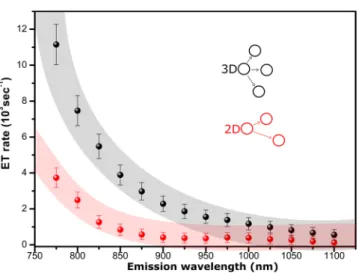
2D structure. In Figure 7, we depict the experimentally determined wavelength dependence of the ΓET; a gradual
increase toward shorter wavelength is observed, indicating a more efficient transfer process for smaller NCs. This is fully consistent with the proposed interpretation of the lifetime reduction in terms of ET, which is more probable for small NCs, as these are more likely to have a larger neighbor available for the ET. In terms of the physical mechanism, we postulate that ET in our systems should be explained in the framework of a phonon-assisted resonant ET process,29whose efficiency is considerably higher than that of the phonon-less process. We recall that eventual electron/hole transfer between NCs, frequently discussed in the literature,30,31is limited to NCs in direct contact with each other and takes place on a picosecond Figure 5.Confirmation of ET. PL effective lifetimes and intensities are depicted as a function of the average number of absorbed photons (Nabs) for
the 3D (a) and 2D (b) arrays of Si NCs. Experimental details are given in theExperimental Section. For both samples, quenching of the effective
lifetimes is observed, coincident with saturation of the PL intensity. The“shaded” traces visualize error margins and function as a guide to the eye. The measurements are performed at a selected PL wavelength of 950 nm, which represents contribution of Si NC of around 5 nm in diameter.
Figure 6. Quantifying ET. The nonradiative recombination rate is plotted as a function of the average number of absorbed photons,Nabs,
(at an emission wavelength of 950 nm). The values are obtained by combining the experimental results given in Figure 5, with the theoretical values of the radiative recombination rates. Upon increase of Nabs, the ET-activated Auger process of excitation quenching is
increased until saturation is reached. The shaded traces function as guides to the eye.
time-scale, and is therefore outside of the scope of this study. The rate of the ET process between Si NCs, identified in this study, is much lower than typically found for direct bandgap materials (∼10 ns in CdSe6), which could explain why its presence remained elusive until now.
To conclude, we explicitly demonstrate ET on the nanometer scale in dense solid state dispersions of Si NCs embedded in SiO2matrix. The identification of ET is based on
the transfer-activated Auger process of excitation quenching. In this way, we directly extract ΓET at a particular emission
wavelength, i.e., for Si NCs of a particular size. The proposed approach can be used to probe ET in similar systems, as long as Auger interactions are significantly faster than the radiative recombination and therefore dominate carrier dynamics. We estimate the characteristic size-dependent time constant of a single ET-event between neighboring NCs and show that it can be changed by dedicated sample preparation. In that way, ET can be effectively engineered. This result opens the way to realization of long-range ET in ensembles of Si NCs and therefore constitutes an essential step toward applications of Si NCs in optoelectronics and photovoltaics.
■
EXPERIMENTAL SECTIONThin film Si NC samples were produced by a magnetron rf cosputtering method using high purity Si (99.99%) and SiO2 (99.99%) targets. The 3D array of Si NCs was constructed by sputtering a 500 nm thickfilm of SiOx, whereas the 2D arrays are built up using 100 cycles made of “active” (SiOx) and
“passive” (pure SiO2) layers, with a thickness of 5 and 10 nm,
respectively. The single layer and all active layers of the multilayer structure were produced with 15 at% of excess Si. The sputteredfilms were annealed for 30 min at 1250 °C in nitrogen atmosphere. This high-temperature heat treatment induces phase separation between Si and SiO2, hence, NC are
formed. TEM and the HRTEM (JEOL JEM-200CX) images have been conducted in the group of Fujii at the University of Kobe. PL spectrum and time-resolved measurements are executed by excitation with a 5 ns, 10 Hz pulsed Nd:YAG laser system (Solar LS), combined with an optical parametric oscillator for excitation energy tunability, and a TRIAX-1000
monochromator (HORIBA Jobin Yvon) coupled to a Hamamatsu photo multiplier tube. Excitation wavelengths of 520 and 355 nm were used to cover a broad range of excitation power regimes. Absorption measurements were carried out using a UV−vis Lambda900 spectrometer in combination with an integrating sphere, accounting for reflection and scattering effects. All spectra were corrected for the system response.
■
ASSOCIATED CONTENT*
S Supporting InformationThe Supporting Information is available free of charge on the
ACS Publications websiteat DOI:10.1021/acs.jpcc.5b06339. (1) A calculation of the radiative recombination rate. (2) Elaborate explanation on the attenuation of the excitation beam through the sample. (3) Monte Carlo simulations to estimate the average nearest-neighbor surface-to-surface distance. (4) Additional power-dependent effective lifetimes. (5) A detailed discussion on the effect of partial saturation. (PDF)
(ZIP)
■
AUTHOR INFORMATIONCorresponding Author
*Phone: (+31) 020-525 6349; e-mail:[email protected](R.L.). Notes
The authors declare no competingfinancial interest.
■
ACKNOWLEDGMENTSWe would like to thank Wouter Meinster for helpful discussions and the Monte Carlo simulations. This work was financially supported by NanoNextNL.
■
REFERENCES(1) Talapin, D. V.; Lee, J.; Kovalenko, M. V.; Shevchenko, E. V. Prospects of colloidal nanocrystals for electronic and optoelectronic applications.Chem. Rev. 2009, 110, 389−458.
(2) Dang, C.; Lee, J.; Breen, C.; Steckel, J. S.; Coe-Sullivan, S.; Nurmikko, A. Red, green and blue lasing enabled by single-exciton gain in colloidal quantum dot films.Nat. Nanotechnol. 2012, 7, 335− 339.
(3) Gregg, B. A. Excitonic solar cells. J. Phys. Chem. B 2003, 107, 4688−4698.
(4) Kamenev, B.; Grom, G.; Lockwood, D.; McCafrey, J.; Laikhtman, B.; Tsybeskov, L. Carrier tunneling in nanocrystalline silicon-silicon dioxide superlattices: A weak coupling model.Phys. Rev. B: Condens. Matter Mater. Phys. 2004, 69, 235306.
(5) Förster, T. Zwischenmolekulare Energiewanderung und Fluo-reszenz.Ann. Phys. (Berlin, Ger.) 1948, 437, 55−75.
(6) Kagan, C. R.; Murray, C. B.; Nirmal, M.; Bawendi, M. G. Electronic energy transfer in CdSe quantum dot solids.Phys. Rev. Lett. 1996,76, 1517.
(7) Achermann, M.; Petruska, M. A.; Crooker, S. A.; Klimov, V. I. Picosecond energy transfer in quantum dot Langmuir-Blodgett nanoassemblies.J. Phys. Chem. B 2003, 107, 13782−13787.
(8) Wuister, S. F.; Koole, R.; de Mello Donegá, C.; Meijerink, A. Temperature-dependent energy transfer in cadmium telluride quantum dot solids.J. Phys. Chem. B 2005, 109, 5504−5508.
(9) Lunz, M.; Bradley, A. L.; Chen, W. Y.; Gunko, Y. K. Two-dimensional Förster resonant energy transfer in a mixed quantum dot monolayer: experiment and theory.J. Phys. Chem. C 2009, 113, 3084− 3088.
(10) Allan, G.; Delerue, C. Energy transfer between semiconductor nanocrystals. Phys. Rev. B: Condens. Matter Mater. Phys. 2007, 75, 195311.
Figure 7. Emission wavelength-dependent ET rate. The ET rate derived from the effective lifetime in the saturation regimeis depicted as a function of the emission wavelength. The ET rate is increased for shorter emission wavelengths, indicating the increased transfer probability for smaller NCs (within the ensemble).
(11) Linnros, J.; Lalic, N.; Galeckas, A.; Grivickas, V. Analysis of the stretched exponential photoluminescence decay from nanometer-sized silicon crystals in SiO2.J. Appl. Phys. 1999, 86, 6128−6134.
(12) Priolo, F.; Franzò, G.; Pacifici, D.; Vinciguerra, V.; Iacona, F.; Irrera, A. Role of the energy transfer in the optical properties of undoped and Er-doped interacting Si nanocrystals.J. Appl. Phys. 2001, 89, 264−272.
(13) Miura, S.; Nakamura, T.; Fujii, M.; Inui, M.; Hayashi, S. Size dependence of photoluminescence quantum efficiency of Si nano-crystals.Phys. Rev. B: Condens. Matter Mater. Phys. 2006, 73, 245333. (14) Gusev, O. B.; Prokofiev, A. A.; Maslova, O. A.; Terukov, E. I.; Yassievich, I. N. Energy transfer between silicon nanocrystals.JETP Lett. 2011, 93, 147−150.
(15) Limpens, R.; Gregorkiewicz, T. Spectroscopic investigations of dark Si nanocrystals in SiO2 and their role in external quantum
efficiency quenching.J. Appl. Phys. 2013, 114, 74304.
(16) Guillois, O.; Herlin-Boime, N.; Reynaud, C.; Ledoux, G.; Huisken, F. Photoluminescence decay dynamics of noninteracting silicon nanocrystals.J. Appl. Phys. 2004, 95, 3677−3682.
(17) Hybertsen, M. S. Absorption and emission of light in nanoscale silicon structures.Phys. Rev. Lett. 1994, 72, 1514.
(18) Dohnalova, K.; Gregorkiewicz, T.; Kusova, K. Silicon quantum dots: surface matters.J. Phys.: Condens. Matter 2014, 26, 173201.
(19) Halivni, S.; Sitt, A.; Hadar, I.; Banin, U. Effect of nanoparticle dimensionality on fluorescence resonance energy transfer in nano-particle-dye conjugated systems.ACS Nano 2012, 6, 2758−2765.
(20) Rabouw, F. T.; den Hartog, S. A.; Senden, T.; Meijerink, A. Photonic effects on the Förster resonance energy transfer efficiency. Nat. Commun. 2014, 5, 3610.
(21) Van Driel, A.; Nikolaev, I.; Vergeer, P.; Lodahl, P.; Vanmaekelbergh, D.; Vos, W. Statistical analysis of time-resolved emission from ensembles of semiconductor quantum dots: Inter-pretation of exponential decay models.Phys. Rev. B: Condens. Matter Mater. Phys. 2007, 75, 35329.
(22) Govoni, M.; Marri, I.; Ossicini, S. Carrier multiplication between interacting nanocrystals for fostering silicon-based photovoltaics.Nat. Photonics 2012, 6, 672−679.
(23) Trojánek, F.; Neudert, K.; Maly, P.; Dohnalová, K.; Pelant, I. Ultrafast photoluminescence in silicon nanocrystals studied by femtosecond up-conversion technique. J. Appl. Phys. 2006, 99, 116108−116108.
(24) Trinh, M. T.; Limpens, R.; Gregorkiewicz, T. Experimental investigations and modeling of Auger recombination in silicon nanocrystals.J. Phys. Chem. C 2013, 117, 5963−5968.
(25) Timmerman, D.; Izeddin, I.; Gregorkiewicz, T. Saturation of luminescence from Si nanocrystals embedded in SiO2. Phys. Status
Solidi A 2010, 207, 183−187.
(26) Valenta, J.; Juhasz, R.; Linnros, J. Photoluminescence from single silicon quantum dots at room temperature.J. Lumin. 2002, 98, 15−22.
(27) Sychugov, I.; Juhasz, R.; Valenta, J.; Linnros, J. Narrow luminescence linewidth of a silicon quantum dot.Phys. Rev. Lett. 2005, 94, 87405.
(28) Kovalev, D.; Diener, J.; Heckler, H.; Polisski, G.; Künzner, N.; Koch, F. Optical absorption cross sections of Si nanocrystals.Phys. Rev. B: Condens. Matter Mater. Phys. 2000, 61, 4485.
(29) Yeltik, A.; Guzelturk, B.; Hernandez-Martinez, P. L.; Govorov, A. O.; Demir, H. V. Phonon-assisted exciton transfer into silicon using nanoemitters: the role of phonons and temperature effects in Förster resonance energy transfer.ACS Nano 2013, 7, 10492−10501.
(30) Lockwood, R.; Hryciw, A.; Meldrum, A. Nonresonant carrier tunneling in arrays of silicon nanocrystals.Appl. Phys. Lett. 2006, 89, 263112.
(31) Belyakov, V., Burdov, V., Lockwood, R., Meldrum, A. Silicon nanocrystals: fundamental theory and implications for stimulated emissionAdv. in Opt. Techn. 2008, p 110.1155/2008/279502.