Susana Filipa Antunes Rodrigues
Intermetallic layer formation and
influence in solder joints reliability
Susana Filipa Antunes Rodrigues
Inter
me
tallic la
yer for
mation and
influence in solder joints r
eliability
Universidade do Minho
Escola de Engenharia
Master Thesis
Integrated Master in Materials Engineering
Supervised by:
Professor Doctor Delfim Fernandes Soares
Professor Doctor José Carlos Fernandes Teixeira
Dr. José Ricardo de Barros Alves
Susana Filipa Antunes Rodrigues
Intermetallic layer formation and
influence in solder joints reliability
Universidade do Minho
Escola de Engenharia
A
CKNOWLEDGEMENTS
This section is addressed to acknowledge all those who gave their contribute to this work and were always available for me.
I would like to acknowledge my supervisor, Professor Delfim Fernandes Soares for their guidance and support, and for being available to help during the development of the present work.
I would like to thank Bosch Car Multimedia, especially to the Engineer José Luís de Sousa Ribas, for his contribution, opportunity, and guidance to carry out this final work. I would also like to all persons from Bosch Car Multimedia by the support during my internship.
I would like to give special thanks to José Ricardo de Barros Alves for all the knowledge, support, dedication and patience.
To my family and friends, a special thanks for encouraging and motivating me throughout this journey.
Thank you all,
A
BSTRACT
Over the years, industries have been experiencing an increasing tendency to reduce the use of nitrogen during the soldering process. Due to this fact, the electronics industry has been investing in the research of cheaper and alternative manufacturing process. This necessity became the motivation for this work, whose purpose is to study of the intermetallic layer formation during soldering processes, and therefore, analyze with accuracy the reliability of solder joints.
The main focus of this study was the analysis of an oxidant atmosphere influence in solder joints reflowed. In the initial stage, a soldering study with an oxidant atmosphere was performed, and the influence of the atmosphere was analyze in specific parameters, such as, the thermal properties, solder joints microstructure, formation and growth of the intermetallic layer. From this analysis, the results revealed that different thermal cycles (heating rates, atmospheres, and maximum temperature) affect the melting temperatures and the thickness of the intermetallic layer. In the second stage, the effect of the oxidant atmosphere was studied in a Bosch Car Multimedia production line. The product, a PCB for a solar panel, was subjected to several inspections steps along the line, namely, solder printing inspection, automatic optical inspection and in circuit test. The results of these inspections showed that the oxidant atmosphere did not have a significant influence in the product reliability and all production was successful. However, it was important to analyze the solder joints in detail. For that, a visual inspection was performed using an optical microscope and microstructural characterization of the solder joints after the soldering process with different atmospheres were conducted.
The experimental results indicate that different atmospheres during reflow soldering did not have influenced the formation and growth of the intermetallic layer. It was also performed an evaluation concerning wettability in a different component in order to study the influence of the oxidant atmosphere. The effect of oxidant atmosphere on contact angle and solder height indicated that the absence of the nitrogen during reflow soldering caused an oxidation of component side and reduce the solder wettability.
R
ESUMO
Ao longo dos anos as indústrias têm vindo a registar uma tendência crescente para reduzir o uso de azoto durante o processo de soldadura. Devido a este facto, a indústria eletrónica tem vindo a investigar processamentos mais baratos. Esta necessidade tornou-se a motivação para este trabalho, cujo objetivo centra-se no estudo da formação da camada intermetálica durante os processos de soldadura e, portanto, analisar com precisão a fiabilidade das juntas de soldadura. O foco principal deste estudo consistiu em analisar a influência da atmosfera oxidante durante a soldadura por Reflow nas juntas de soldadura. Na fase inicial, foi realizado um estudo da solda com uma atmosfera oxidante e na qual a influência foi estudada nos parâmetros como, as propriedades térmicas, microestrutura das juntas de soldadura e na formação e crescimento da camada intermetálica. A partir desta análise, os resultados revelaram que para diferentes ciclos térmicos (variação da velocidade de aquecimento, temperatura máxima e atmosfera) as temperaturas de fusão e as camadas intermetálicas foram afetadas.
Na segunda fase foi estudado também o efeito de uma atmosfera oxidante numa linha de produção da Bosch Car Multimedia. O produto escolhido, uma placa de circuito impresso de um painel solar, foi submetido a várias etapas de inspeção ao longo da linha, ou seja, a inspeção da impressão de pasta, uma inspeção ótica automática às juntas de soldadura e um teste ao circuito da placa. Os resultados destas inspeções mostraram que o uso de uma atmosfera oxidante não teve uma influência significativa na fiabilidade uma vez que toda a produção foi realizada com sucesso. No entanto, é necessário realizar uma análise em detalhe às juntas de soldadura. Para tal, foi realizada uma inspeção visual e uma caracterização microestrutural das juntas de soldadura através do uso do microscópio ótico e eletrónico.
Os resultados experimentais obtidos indicam que diferentes atmosferas durante a soldadura por Reflow não teve uma influência significativa no crescimento e formação da camada intermetálica. Foi também realizada uma avaliação da molhabilidade em diferentes componentes a fim de estudar a influência da atmosfera oxidante. O efeito da atmosfera oxidante sobre o ângulo de contacto da solda e altura mostrou que a ausência de azoto durante a soldadura por Reflow causou uma oxidação do lado do componente uma vez que molhabilidade reduziu.
Palavras-chave: Camada intermetálica, Atmosfera oxidante, Junta de soldadura, Soldas sem chumbo, Ciclo térmico
INDEX
Acknowledgements ... iii Abstract ... v Resumo ... vii List of Figures ... xi List of Tables ... xvList of Abbreviations and Acronyms ... xvii
Chapter 1 Introduction ... 1
1.1. Motivation ... 1
1.2. Objectives ... 1
1.3. Structure of the Thesis... 2
Chapter 2 Literature review ... 3
2.1. Printed Circuit Board (PCB) ... 3
2.1.1. Classification of PCBs ... 3
2.1.2. PCB surface finishes ... 5
2.2. PCB assembled (PCBA) ... 7
2.2.1. Electronic components ... 7
2.2.2. Surface mount technology (SMT) ... 8
2.2.3. Through-hole technology (THT) ... 9
2.3. Fluxes ... 9
2.4. Solder alloys ... 11
2.4.1. Commercial solder alloys ... 11
2.5. Soldering techniques in electronic packaging industry ... 12
2.5.1. Reflow soldering process ... 12
2.5.2. Wave soldering ... 16
2.6. Solder joints ... 18
2.6.1. Intermetallic compound (IMC) ... 18
Chapter 3 Experimental Procedures ... 25
3.1. Introduction... 25
3.2. Soldering study with an oxidant atmosphere ... 25
3.2.1. Materials ... 25
3.2.2. Methods ... 26
3.2.3. Characterization techniques ... 27
3.2.4. Morphological analysis ... 28
3.3. Oxidant atmosphere study in a production line ... 30
3.3.1. Materials ... 30
3.3.2. Methods ... 31
3.3.3. Product validation ... 35
3.3.4. Morphological characterization ... 38
Chapter 4 Results and discussions ... 43
4.1. Soldering study with an oxidant atmosphere ... 43
4.1.1. Thermal analysis ... 43
4.1.2. Microstructural analysis of the interface ... 47
4.1.3. Formation and growth of intermetallic layer at the interface between SAC and Sn substrate ………53
4.2. Oxidant atmosphere study in a production line ... 56
4.2.1. Solder paste inspection ... 56
4.2.2. Automated optical inspection ... 59
4.2.3. In circuit test ... 60
4.2.4. Visual Inspection... 60
4.2.5. Characterization of solder joints ... 62
Chapter 5 Conclusions ... 73
Chapter 6 Future work ... 77
References ... 79
Annex I ... 83
L
IST OF
F
IGURES
Figure 2.1 PCB schematic representation [6]. ... 3
Figure 2.2 Three main categories of printed circuit board: a) single-sided, b) double-sided and c) multi-layered [5]. ... 5
Figure 2.3 The function of the flux in soldering [19]. ... 10
Figure 2.4 Market solders lead: a) Different lead-free solders in the market and b) different types of SAC alloys [11]. ... 12
Figure 2.5 PCBAs production line [6]. ... 13
Figure 2.6 Schematic representation of the stencil printing machine [16]. ... 13
Figure 2.7 Typical reflow profile for lead-free Sn-Ag-Cu solder paste [21]. ... 15
Figure 2.8 Wave soldering of a PCB [24]. ... 17
Figure 2.9 Constituents of the solder joints. ... 18
Figure 2.10 Optical micrograph of the solder/substrate interconnection [29]. ... 20
Figure 2.11 The ternary phase diagram of Sn-Ag-Cu alloys [11]. ... 20
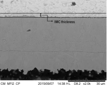
Figure 3.1 SEM image for IMC thickness measurement. ... 29
Figure 3.2 Schematic representation about the Solar A production. ... 30
Figure 3.3 Reflow process steps: a) EKRA X4 professional machine Bosch edition, b) Siemens Siplace S20, and c) REHM Inert Gas Reflow Soldering System VXP 3500. ... 32
Figure 3.4 Reflow profile and the results obtained on the different zones. ... 33
Figure 3.5 SMT adhesive curing: temperature profile. ... 34
Figure 3.6 Wave soldering process: a) Universal Radial type 8, b) Siemens G2 equipment and c) EPM CIG 400. ... 34
Figure 3.7 Wave thermal profile. ... 35
Figure 3.8 Koh-Young Machine (SPI equipment). ... 36
Figure 3.9 AOI equipments. a) Viscom 6056 8M, b) Marantz M22XDL350. ... 37
Figure 3.10 Reer ICT equipment. ... 37
Figure 3.11 Cross-sectional zones. ... 38
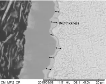
Figure 3.13 SEM image for IMC thickness measurement between solder and substrate. ... 40
Figure 3.14 SEM image for IMC thickness measurement between solder and component. ... 41
Figure 3.15 Micrograph and SEM image of electrolytic with specific zones where were made IMC thickness measurement. ... 41
Figure 3.16 SEM image for solder height measurement. ... 42
Figure 4.1 DSC curves, with different heating rates, under an oxidant atmosphere. ... 44
Figure 4.2 DSC curves, with the same heating rate, under an inert and oxidant atmosphere. ... 44
Figure 4.3 Graph about start of melting temperature as a function of the heating rate for SAC405. ... 46
Figure 4.4 Graph about the end of melting temperature as a function of the heating rate for SAC405. ... 46
Figure 4.5 SEM micrographs of SAC305 for different temperatures, 240, 250 and 260 ºC, under inert and oxidant atmospheres. ... 48
Figure 4.6 SEM micrograph of the solder joint with SAC305 and Sn substrate a) and EDS element mapping for all the elements b), for Sn c) Cu d) Ag e) and Al f). ... 49
Figure 4.7 EDS spectra of IMC layer. ... 50
Figure 4.8 SEM micrographs of SAC405 for different temperatures, 240, 250 and 260 ºC, under inert and oxidant atmospheres. ... 51
Figure 4.9 a) SEM micrograph of the solder joint with SAC405 and Sn substrate a) and EDS element mapping for all the elements b), for Sn c) Cu d) Ag e) and Al f). ... 52
Figure 4.10 EDS spectra of intermetallic layer. ... 52
Figure 4.11 Average of IMC thickness for SAC305 as a function of maximum temperature. ... 53
Figure 4.12 Average of IMC thickness for SAC405 as a function of maximum temperature. ... 54
Figure 4.13 Results about SPI (height) for different components. ... 57
Figure 4.13 Results about SPI (height) for different components (continued). ... 58
Figure 4.14 Number of pseudo-errors detected in AOI. ... 59
Figure 4.15 Visual inspection of PCBAs after reflow and wave in an inert and oxidant atmosphere. ... 61
Figure 4.16 Evaluation of solder joints in capacitor component, under different atmospheres and after reflow and wave soldering. ... 62
Figure 4.17 Evaluation of solder joints in resistor component, under different atmospheres and after reflow and wave soldering. ... 63 Figure 4.18 Evaluation of solder joints in QFP component, under different atmospheres and after reflow and wave soldering. ... 63 Figure 4.19 Evaluation of solder joints in the electrolytic component, under different atmospheres and after reflow and wave soldering. ... 63 Figure 4.20 SEM micrograph of capacitor solder joint a) and EDS element mapping corresponding Sn b), Cu for c), Ag d), Ni e) and Al f). ... 64 Figure 4.21 EDS general mappings of capacitor solder joint with different conditions: a) Reflow (inert atmosphere), b) Reflow (oxidant atmosphere), c) Wave (after reflow with an inert atmosphere) and d) Wave (after reflow with an oxidant atmosphere). ... 65 Figure 4.22 Average of IMC/PCB thickness in solder joints for SMD components as a function of soldering processes. ... 66 Figure 4.23 Average of IMC/PCB thickness in solder joints for TH component in different zones as a function of soldering processes. ... 67 Figure 4.24 Average of IMC/Component thickness in solder joints for SMD components as a function of soldering processes. ... 69 Figure 4.25 SEM micrograph of QFP solder joint a) and EDS element mapping general b), Sn for c), Cu d), Ag e) and Ni f). ... 70 Figure 4.26 Contact angles of the resistor, capacitor and QFP components measured as a function of atmosphere used. ... 71 Figure 4.27 Solder height in the QFP component fabricated in inert and oxidant atmosphere. .. 72
L
IST OF
T
ABLES
Table 2.1 SMD and TH components... 8
Table 2.2 Different IMCs formed between SAC alloy and substrates [2, 30]. ... 21
Table 2.3 Defects which can appear in PCBAs after soldering [33-35]. ... 22
Table 3.1 Composition, melting point and density corresponding to SAC305 and SAC405. ... 26
Table 3.2 Thermal cycle used for SAC305 and SAC405. ... 27
Table 3.3 Heating-cooling DTA profile used for SAC405. ... 27
Table 3.4 Data about the soldering process, reflow and wave. ... 31
Table 3.5 The temperatures defined on reflow oven. ... 33
Table 4.1 Results of DTA analysis for different heating rates and different atmosphere. ... 45
Table 4.2 Number of pseudo-errors after reflow and wave soldering with an inert and oxidant atmosphere. ... 60
Table 4.3 Average IMC/PCB thickness for the capacitor, resistor and QFP components with different conditions. ... 66
Table 4.4 Average IMC thickness of electrolytic component with different conditions. ... 68
Table 4.5 Average IMC/Component thickness for the capacitor, resistor and QFP components with different conditions. ... 69
L
IST OF
A
BBREVIATIONS AND
A
CRONYMS
Ag Silver
Al Aluminum
AOI Automatic Optical Inspection
Cu Copper
DTA Differential Thermal Analysis
EDS Energy-dispersive X-ray Spectroscope ENIG Electroless Nickel Immersion Gold FR4 Flame Retardant 4
g Gramm
IMC Intermetallic compound Imm. Sn Immersion Tin
kV Kilovolt
LFHASL Lead-Free Hot Air Solder Leveled
m Meter mg Milligram min Minute mm Millimeter Ɵ Angle ºC Degree Celsius
OSP Organic Solderability Preservatives PCB Printed Circuit Board
PCBA Printed Circuit Board assembled ppm Parts per million
PTHs Plated through-hole QFP Quad Flat Pack
s Second
SAC Sn-Ag-Cu
SEM Scanning Electron Microscope SMD Surface Mounted Device
SMT Surface Mount Technology
Sn Tin
SPI Solder Printing Inspection TH Through-hole
THT Through-hole Technology
1.
C
HAPTER
1
I
NTRODUCTION
1.1. Motivation
Currently, the market is more competitive and requires companies to be more effective and flexible on price. With the emergence of reducing the costs in an electronics manufacturing, the electronic industry has studied cheaper alternatives.
Nitrogen atmosphere has been used for a long time in the production line and the using this atmosphere has as objective the oxidation reducing of the solder and improve the solderability [1]. However, the costs associated to the use of nitrogen atmosphere are high and the Bosch Car multimedia is spending 1 million euros by year in nitrogen.
The solder joints play an important role in electronic manufacturing, serving both as electrical interconnections and mechanical support between the components and the PCB [2]. The change of inert atmosphere for oxidant atmosphere in the soldering process can bring a substantial impact in the solder joint reliability. Therefore, when the industry thinks into changing the atmosphere, is necessary to understand the causes behind this change. The use of oxidant atmosphere during soldering process has many disadvantage such as solder oxidation, wetting reducing, increase the number of defects, among others [3]. There are several issues that need to be reevaluated and readjusted in the process windows. For such, the evaluating of the atmosphere effect on the soldering performance of lead-free solders is an important factor. Therefore, this evidence became the motivation for this work, whose purpose is to study the intermetallic layer formation and the influence in solder joints reliability, which may posteriorly serve as a basis for others investigations.
1.2. Objectives
Due to the fact of the high cost associated to the nitrogen used during soldering processes, alternatives have been investigated for reducing these costs. Thus, an alternative proposed by Bosch Car Multimedia was the removel of the nitrogen during reflow soldering process. Therefore, with this project it is intended to achieve the following objectives:
Evaluation of the intermetallic layer in function of different conditions, such as, thermal cycles, atmospheres and the solder type;
To study the effect of reflow atmosphere on the intermetallic layer formation and the solder joint reliability.
1.3. Structure of the Thesis
The present thesis includes two different projects which were developed in two institutions, University of Minho and Bosch Car Multimedia. This thesis is a result of collaborative research work carried out by me, Susana Rodrigues, Professor Delfim Soares and José Ricardo Alves.
The Master’s thesis is based in the study of the intermetallic layer formation and the influence of oxidant atmosphere in the solder joints reliability. This way, the thesis is divided into 6 chapters.
In Chapter 1 is presented the motivation to performed this study and objectives to achieve during the work.
Chapter 2 approaches the literature review where it is explained the manufacturing processes and the essential background concepts concerning the soldering.
A description of the work carried out are presented in Chapter 3 and this are divided into two projects, soldering study with an oxidant atmosphere (performed at University of Minho) and oxidant atmosphere study in a production line (performed at Bosch Car Multimedia).
Chapter 4 presents the results and related discussions and Chapter 5 presents a conclusion of the work performed along this Master Degree.
2.
C
HAPTER
2
L
ITERATURE REVIEW
2.1. Printed Circuit Board (PCB)
Printed circuit boards are the products used in the interconnection technology in electronic products. It is through this product that can be made the connection between the components in an electronic circuit. Thus, these are products with a vast expansion in the market due to its function [4].
The essential components in the printed circuit board are the base and conducting tracks (circuits). The PCB base, which is a thin board of insulating material, rigid or flexible, provides mechanical support to all components which make up a circuit. Regarding to the circuit, this is formed by a thin layer of conducting material, usually copper, deposited on the surface the substrate. These circuits provide the electrical connection between components and base [4, 5].
The base used is constituted by glass fiber reinforced epoxy resin designated Flame Retardant (FR4). The conductors, pads, and vias are constituted by copper. The components soldered to pads on the surface of the circuit board are designated as surface mounted device (SMD). However, there are vias were can be inserted and soldered component to the PCB which are designated as through-hole (TH), as shown in Figure 2.1 [4].
Figure 2.1 PCB schematic representation [6].
2.1.1. Classification of PCBs
The PCB classification is based on the number of layers printed and to the presence or absence of plated-through holes. Thus, there are three types of PCBs construction (Figure 2.2):
SMD Component Tracks FR4 Pads Vias (TH) Copper layers
Single Sided PCB´s consists in the simplest and the cheapest type of boards that contain a single layer of copper on one side of an insulating base material. This type of PCB can be used for through-hole and surface mount components. In a through-hole single-sided printed circuit board, components are situated on the non-track side of the circuit board while their leads go through the through-holes to the other side, where they are soldered to lands. In a surface mounted printed circuit board, components are situated on the same side of the board as the copper track [4, 5].
Double Sided PCB´s consist of two copper layers on both sides of the insulating base material. Thus, in this PCB is possible to have more density of components and the conductor tracks are higher than the single sided boards.
This type of PCB can be used for both through-hole and surface mount components. In a through-hole double-sided assembly, components are usually situated on just one side and soldered on the other. Where through-holes are required to interconnect top and bottom copper track layers, they are placed inside the hole with copper and are called plated through vias. Where a component lead also goes through a via it is called a plated through-hole (PTHs).
In a surface mounted double-sided assembly, components are on the same side as boards are soldered. Components may be mounted on both sides of the board. It is important to note that only there is an electrical connection between the two sides when used plated through-hole [4, 5].
Multi-layered PCB´s is constituted by a substrate with layers of printed circuits separated by layers of insulation. The current products tend to add greater numbers of features in a smaller PCB area. Therefore, these PCBs are used where the density of connections needed is too high to be handled by two layers. Plated through-holes can be used for either component terminal connection, or just as electrical connections (in which case they are called vias). Vias passing from one outside track to the other are called through vias while those connecting internal track layers are called blind, or buried vias [4, 5].
Figure 2.2 Three main categories of printed circuit board: a) single-sided, b) double-sided and c) multi-layered [5].
The PCBs can also be classified on the basis of the type of insulating material used, i.e. rigid, flexible or rigid-flex. The rigid boards is composed of a variety of materials and the flexible boards are constituted by a substrate material like polyester or polyamide. The rigid-flex boards consist in a rigid and flexible substrates laminated together into a single structure [4].
2.1.2. PCB surface finishes
The surface finish can be defined as a coating, either metallic or organic in nature. The effect of surface finish is the important factor that causes differences in the microstructure and mechanical properties between solder joints.
Copper is used as a base metal conductor in the fabrication of printed circuit board. This metal has excellent properties as a conductor of heat and electricity. However, the copper oxidizes and deteriorates in the presence of water and air. This way, if the copper surface on the PCB is not coated or treated with a protective agent, the exposed area would rapidly become unsolderable [4].
Therefore, the surface finish is applied to a PCB in order to assure solderability of the metal. This protective finish must be solderable and act as a barrier for preventing the copper from oxidizing. Thus, it is possible to provide a solderable surface when assembling the components to the printed circuit board [4, 7].
The most commonly PCB surface finishes used in Bosch Car Multimedia are detailed below.
Immersion Tin (Imm. Sn)
Immersion Tin is a metallic surface finish that is considered to be very good in terms of corrosion resistance and its cost is competitive. This process consists in immersion tin bath, it continues to build up in thickness over time. The thickness is on the order of 0.1 to 1.5 μm [8].
This surface finish is used for replacing and protect the solderability of copper surfaces and in that way extend the shelf life of the board [9]. Over time, the tin forms an intermetallic compound with Cu at a rate that is dependent on temperature. If the intermetallic reaches the coating surface, it oxidizes rapidly resulting in poor solderability of the solder joint area [8, 10].
Lead-Free Hot Air Solder Leveled (LFHASL)
Lead-free HASL is a novel surface finish which is currently being implemented by industry in order to respect the new directives implemented by the European Union. These new regulations require that lead has to be removed from any end-of-life electrical or electronic components [11]. The LFHASL process consists in the application of flux to the PCB, and subsequently, immersing it in a molten pot solder at approximately 265ºC. Afterwards, the hot air knives blow the excess molten solder of the pads. The typical thickness of the LFHASL may vary between 0.6 to 51 μm [12, 13].
LFHASL has the key advantage of achieving excellent solderability because “Nothing solders like solder”. The products with LFHASL surface finishes possess an excellent shelf life and has high solderability even after two surface mount profiles. The LFHASL surface finish is slightly more planar than HASL and it gets wet faster [8].
Organic Solderability Preservatives (OSP)
OSP, as the name implies, is an organic coating that protects the copper from oxidation on the solderability process. The typical thickness is 0.2 to 0.5 µm.
In the soldering process, the organic coating is penetrated, dissolved and removed by the flux during soldering. Therefore, at high temperatures, OSP is not as robust as the other metal finishes and has a smaller process window [8, 14].
The HASL tends to be able replaced by OSP because this surface finish has advantages as stronger solder joint, substrate low price, is environment-friendly, simple process, provides a surface planarity equivalent to the plated copper finish, and require very low equipment maintenance [7, 9, 14].
Electroless Nickel Immersion Gold (ENIG)
In this surface finish (according to the Bosch specifications), a layer of electroless nickel with a thickness of 4 to 9 µm is deposited on the copper and is the surface to which the soldering occurs. The immersion gold is the layer that protect the nickel from oxidation during storage and has a thickness of 0.05 to 0.15 µm [9, 15].
This surface finish are attractive because it presents a good flat coplanar surface, has excellent solder wettability characteristics, is an ideal surface for pad contacts and improve shelf life over other surface finishes [9].
ENIG is known to have good solderability but, on the other hand, it has high cost and the susceptibility to black pad issues. Black pad is a phenomenon related to some weak solder joints on ENIG surface finish [12].
2.2. PCB assembled (PCBA)
The PCBA refers to the PCB after the soldering process. It means that on this stage the components are electrical and mechanical connected to the board [4].
The Bosch Car Multimedia is one of the companies responsible for PCBA mounting since PCBs, components and solders are purchased from other companies.
The PCBA can be done manually or by using machines which make the assembly process automatic, fast and reliable. It is important to refer that exist different products which play different functions, the components and the soldering process used can be different. Thus, the final product of assembled PCB consists of a lot of different types of components with many configurations, an assembly process must be selected of according with cost and the reliability [4].
2.2.1. Electronic components
The electronic components can be defined as a material that handles electricity. The electronic industry makes use of a variety of components. These components can have many
shapes, sizes and perform different electrical functions depending upon the purpose for which they are used [4].
Components can be classified into two types, surface mount device, and through-hole. This classification is based on the basis of the method of their attachment to the circuit board. The components leaded directly onto the surface of the board are designed by surface mount components. When the components leaded by inserted through mounting holes in the circuit board these are considerate through-hole components [4].
On the Table 2.1 can see different types of components, SMD, and TH, used in electronic equipment.
Table 2.1 SMD and TH components.
Surface mount components Through-hole components
2.2.2. Surface mount technology (SMT)
Surface mount technology is a revolutionary change in the electronics industries. Surface mount technology dates back to the 1960s when it was developed for hybrid microcircuit assemblies for which it was difficult to put holes into the ceramic substrates. The advance of surface mount technology for the laminate substrate, though, is relatively recent. Thus, the surface mount technology emerged due to advantages of being able to place components on both sides of the PCBs.
Surface mount technology is based in the components soldered to pads on the surfaces of the circuit board. This technology present advantages as a higher degree of automation that
QFP (Quad Flat Pack)
Chip capacitor
Electrolytic
result in a lower manufacturing cost, inclusion the smaller components which imply smaller volume, higher circuitry, and better performance [4, 16, 17].
2.2.3. Through-hole technology (THT)
Through-hole technology consists on the process by which component leads are inserted into holes in the circuit board and soldered into place.
This technology has been used since early in the electronic industrial (the 1920s) when the component was soldering point-to-point. In 1960, this process had one progress with the emergence of wave soldering process.
The main disadvantage of this technique is the low assembly densities, which led to the introduction of surface-mount technology.
On the other hand, through-hole components are used for high-reliability products that require strong connections between layers. There are many reasons why through-hole technology is used over surface mount including the size and shape of the component, the leads placement, and even the sensitivity and stress of component. This technology is used by military and aerospace products because are exposed to extreme accelerations, collisions, or high temperatures [9].
2.3. Fluxes
Flux is a substance used in the soldering process which cleans the surfaces to be soldered. The flux function is to remove oxides and other nonmetallic impurities (Figure 2.3). The majority of the metals tend to form compounds with atmospheric oxygen which leaves a coating of oxide even at room temperature, gold and platinum are exception. The oxidation rate can increase if there is a temperature and humidity increase. However, soldering flux has several functions to perform, such as:
React with oxide and other contamination on the surface to be soldered
Dissolve the metal salts formed during the reaction with the metal oxides
Protect the surface from re-oxidation during the soldering process
Provide a thermal blanket to spread the heat evenly during soldering
Reduce the surface tension of the melted solder in order to enhance wetting
These fluxes contain different types of ingredients capable of performing these functions, such as:
Activators: are present in the flux formulation to enhance the removal of metal oxide presents in the surfaces to be soldered. The activators are usually acids or compounds that release acids at elevated temperature. The activity of the activators increases with temperature during the preheat step of the soldering process, up to a certain value where their activity concludes, either due to thermal decomposition or excessive volatilization.
Vehicle: is a solid or nonvolatile liquid that acts as an oxygen barrier protecting the metal surface against oxidation. This ingredient dissolves the metal salts formed in the reaction of the activators with the surface metal oxides and carry them away from the metal surface. Provide to a heat transfer medium between the solder and the components or PCB substrate.
Solvent: serves to dissolve the vehicle, activators, and other additives. Solvents evaporate during preheating and before the soldering operation.
Additives: can be other ingredients that serve a specialized function. These ingredients can enhance the wetting properties by decrease the interfacial surface tension between the molten solder and the PCB, provide good viscosity, low slump during the preheat step, among others effects [5, 9, 18].
Figure 2.3 The function of the flux in soldering [19].
The fluxes can be classified as, rosin fluxes, water-soluble fluxes or “no-clean fluxes”. The rosin fluxes can be non-activated (R), mildly activated (RMA) and activated (RA). RA and RMA are the fluxes which contain rosin combined with an activating agent (an acid) which increases the wettability of metals by removing the oxides presents. Regarding the water–soluble fluxes, they need to be cleaned after the soldering because these fluxes present higher activity. The “no-clean” fluxes are mild enough to not require removal due to their non-conductive and non-corrosive residue [5, 9].
2.4. Solder alloys
With the development of electronics industry, Sn-Pb solder was used as the interconnect material of electronic components to the PCB. These solders were predominant choice of the electronics industry because provide excellent solderability and reliability of the solder joint. However, the lead present in solder was considered a toxic substance that causes several negative impacts on the environment and human body. Thus, due to the problems that this causes the legislation required the removal of lead in the electronics industry. The European Union in June 2000 adopted two directives, the "Waste of Electrical and Electronic Equipment (WEEE)" and "Restriction of the Use of Certain Hazardous Substances (RoHS)". The first requires the removal of lead in all the electronic and electrical components at the end of life and the second directive prohibits the use of lead in electrical components and electronic manufactured after July 1, 2006 [11].
To be considered an alternative to Sn-Pb solders these should be lead-free candidates with similar or better properties. Therefore, for a Sn-Pb solder to be replaced the electronic industry to take account of the advantages that this solder (Sn-Pb) guarantee, such as the following:
Reduction the surface tension of pure tin in that way improving wettability
Provide ductility to Sn-Pb solders
Allowing the rapid formation of intermetallic compounds by tin and copper diffusion
Allowing the use of low processing temperature due to its low melting point
Low cost and very abundant material
Therefore, as lead has the disadvantage of toxicity electronics industry had to replace to other alternatives. Thus, it appeared on the market lead-free solders which presents similarities to Sn-Pb solder [11].
2.4.1. Commercial solder alloys
The lead-free solder needs to have a low melting point, in order to have a similar reflow profile during the manufacturing process; good wetting ability to ensure good metallization; good electrical properties to efficiently transmit electrical signals; and adequate mechanical properties to preserve the reliability of solder joints, i.e. good bonding of electronic components on the printed circuit board. The new lead-free solders also need to be non-toxic and low-cost. Thus, after several types of research and studies, the solders that have similarities with Sn-Pb solders are the Sn-Ag,
Sn-Ag-Cu (SAC), and other alloys containing elements such as tin (Sn) , silver (Ag), copper (Cu), bismuth (Bi), indium (In) and zinc (Zn), as shown in Figure 2.4a [11].
Several SAC alloys have been proposed by electronic industry. These included SAC305 (96.5-3.0Ag-0.5Cu), to SAC387 (95.5Sn-3.8Ag-0.7Cu), SAC396 (95.5Sn-3.9Ag-0.6Cu) and the SAC405 (95.5Sn-4.0Ag-0.5Cu), as shown in Figure 2.4b. These solders have some benefits for examples, low melting temperatures compared with the 96.5Sn-3.5Ag, as well as their superior mechanical and solderability properties when compared to other lead-free solders [11].
Figure 2.4 Market solders lead: a) Different lead-free solders in the market and b) different types of SAC alloys [11].
2.5. Soldering techniques in electronic packaging industry
Soldering is a method used to produce permanent electrical and mechanical connection between substrate and components. There are many different soldering practices employed in the electronic packaging industry. They all involve four basics ingredients: base metals, solder material to the joining components, flux and heat. By far the commonest methods of soldering used by electronic packaging industry are reflow soldering and wave soldering.
2.5.1. Reflow soldering process
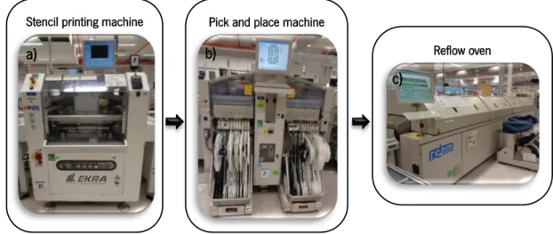
The reflow soldering process consists in solder electronic components (SMD) on the PCB. This process consists in three main steps: the solder printing, the components placement and the reflow soldering. Figure 2.5 shows an integrated manufacture line for electronics boards.
Figure 2.5 PCBAs production line [6].
2.5.1.1. Solder paste printing
The first step, stencil printing process, consists in the application of the solder paste on the PCB using a stencil. The stencil is formed of metal foil with a pattern of aperture matching the footprint on the PCB. This stencil is positioned above the board and a squeegee drawn over the stencil forcing the solder paste through the screen apertures and the solder paste is deposited on top of the corresponding pads (Figure 2.6). It is important to refer that the solder paste provides some adhesive qualities during transportation of the board before soldering to prevent component misalignment or loss.
Figure 2.6 Schematic representation of the stencil printing machine [16].
This process requires a flat substrate for the stencil to be laid on and present advantages as higher speed, higher throughput, and better solder paste volume and better pattern registration [16, 20].
2.5.1.2. Component placement
After the solder paste has been printed, the PCB is then transported for the production line Solder printing
SPI (Solder printed inspection)
Componentplacement Reflow soldering
correctly and placed it onto the PCB pads, where the solder paste secures the component in place during other processes of the board assembly. This process used automatic vision viewing and alignment technology. These machines are used because they present high speed in order to maximize the production volume and high precision placement of a whole range of electronic components [9, 16, 20].
2.5.1.3. Reflow soldering
Reflow soldering is the step in which a PCB, which has the components placed on the solder deposit is passed through an oven in order to melt the solder and form the solder joints.
The methods used for reflow soldering are forced convection, infrared, and vapor phase. The method used at Bosch Car Multimedia is forced convection reflow. Reflow equipment contains typically about 8 to 10 heating zones with temperature control to handle large complex assemblies. During the soldering, the assemblies are transported through the oven by a conveyor line. Forced convection reflow consist in an oven, where the heating of the PCB is made through the forced convection. This soldering process is based in the transfer of heat via a flow of gases [10, 16].
Reflow ovens are divided into the following four zones: preheat, soak, reflow and cooling (Figure 2.7).
Preheat
During this stage the volatile material in the flux evaporate. Initially, the PCB and components are heated up gradually from room temperature to about 170 ºC. The ramp rate is a critical parameter so it should be controlled between 1-3 ºC/sec. This way, slow heating minimize thermal shock to the PCB and the components electronic [10].
Soak
This stage should be considered as a continuation of the preheat stage. The flux is activated and it cleans the surface oxides on the solder particles, pads, and components leads. Also, activated flux continues to keep the metal surfaces away from re-oxidizing. The temperature is maintained between 170 to 220 ºC, during an extended period. This stage had as aim to reduce the temperature difference between the large and small mass components on the assembly during reflow [10].
Reflow
The PCBA enters the reflow stage where the solder particles melt and result in the soldering between the PCB and components terminations. On this stage the temperature rises over the liquidus temperature of the solder paste between 217 to 221 ºC for lead-free alloys. Normally the
range of peak temperature is 235 to 250 ºC and the range of time above liquidus is between 45-75 seconds, this way it is possible to provide adequate time for wetting and formation of a quality solder joint. This stage should be controlled because if the temperature and times above referred are exceed it can result in a potential PCB/component damage. Other possible failure is the excessive intermetallic compound (IMC) formation, making the solder joint more brittle [10].
Cooling
After the formation of all solder joints, the assembly is cooled down to room temperature. This step determines the grain structure during solidification. A fast cooling rate forms a finer grain structure (normally 3 to 4 ºC/sec.). A slow cooling results in a larger grain size that may have poor fatigue resistance. This way, the fast cooling is chosen because it presents better mechanical properties due to the fine grain structure [10].
Figure 2.7 Typical reflow profile for lead-free Sn-Ag-Cu solder paste [21].
2.5.1.4. Inert and oxidant atmosphere
To avoid high rate oxidation during the soldering process an inert gas can be used. At Bosch Car Multimedia the inert gas used is nitrogen.
Nitrogen is a common gas found in the atmosphere (about 78% of the Earth’s atmosphere). The soldering process with an inert atmosphere protect metal surfaces from oxidation during heat-up and assuring proper action of flux. Nitrogen is used to displace oxygen because it is the
chemically unreactive [22]. This way, nitrogen is used for many years in the soldering process and it presents several benefits, such as:
Reduce oxidation during the joining process ensuring the solder wetting
Elimination of the oxides formation improving the wettability
Reduce the defects number
Avoid the use of solder paste with high fluxing capacity which improve quality and cleanliness of the solder joints [22, 23]
However, at Bosch Car multimedia are spending about 1 million euros by year in nitrogen. The used of nitrogen is considered an additional cost in soldering process and this way it was decided to study the soldering process without nitrogen. Thus, an alternative to reduce costs is to use an air atmosphere in reflow.
Although the costs reduction an oxidant atmosphere, especially at high temperatures, cause most metals to oxidize, this way the soldering flux in the system has to work more to remove the oxidation on the pad. Thus, the presence of oxygen during the reflow soldering results in poorer solderability.
The soldering process with an oxidant atmosphere is a problem for wettability, mainly for the second side to be soldered once that after the first reflow the PCB surface of the second side is already oxidized [16]. On the other hand, in the first reflow the oxidation problems can appear in the components lead and the other side of the PCB.
2.5.2. Wave soldering
The wave soldering is a method used to solder through-holes components and some surface mounted components onto PCBs (Figure 2.8). These components are soldering when the PCB passes over a wave solder. Wave soldering is used for both, through-hole and surface mount printed circuit assemblies. Firstly, there is the insertion of components in the PCB. This insertion can be by radial leaded and manual assembly. The radial leaded components is an automatic insertion which insert the components into the printed circuit board in the proper order. Regarding the manual assembly these components are installed manually by operators. This operators install a few components and then slide the PCB to the next operator via a conveyor [9].
Fluxing
The first stage consists in the application of the flux on the surface of the PCB assembly. The PCB is moved by conveyor where is to be applied flux by foam or spray. This flux is applied for improve the wetting of surfaces and to protect the metal parts from oxidation during soldering.
Preheating
This stage consists in preheating the PCB where the flux is activated and evaporation of its volatiles. This stage has the role in minimizing the thermal shock before the wave soldering operation. The top of the board should reach a minimum of 100-120 ºC before the next step, wave soldering, in order to avoid thermal shock.
Wave soldering
This stage, the components are soldered to the board using the solder wave. The wave soldering process is ideal for the through-holes components and some surface mount boards that use larger components. For lead-free the solder temperature should be between of 260-270 ºC. There are several types and shapes of waves that can be used for single and dual waves. In this case, the process used is a dual wave where the first wave is a turbulent and second wave is laminar. The turbulent wave ensures the wetting of all leads while the laminar wave removes excessive solder the way to control the meniscus of the molten solder at each joint. This process is usually used when SMDs are to be soldered in the bottom of the board. This machine can have coupled a hot air knife. The force of the air helps to remove excess solder reducing solder bridges as shown in Figure 2.8 [4, 5, 16].
2.6. Solder joints
The formation of solder interconnections in electronic packages implicates the melting of solder in contact with a metal surface. Thus, the solder joints play an important role in electronics packaging, serving both as electrical interconnections and mechanical support between the substrate (PCB) and the components. As technology advanced, the size of the components used have decreased and, as a result, the number of solder joints increased. These solder joints are also required to have the capacity to remove heat from joined devices. In addition, one of the most important factors which are known to influence solder joint reliability is the intermetallic compound layer formed between the solder and the substrate. Figure 2.9 shows the parts that constitute a solder joint [2, 25].
Figure 2.9 Constituents of the solder joints.
2.6.1. Intermetallic compound (IMC)
In the soldering process, there are interfacial reactions between two different materials. The liquid solder reacts with the base metal and forms an IMC layer, which is the bond between the two materials. The solder joint formed at the solder/substrate interface is affected by diffusion rate of a metal substrate (Cu) into the molten solder. This way, the intermetallic layer presence is an indicator of the metallic bonding and, therefore, represents one the most important factors in the soldering process because they influence solder joint reliability [20, 26].
It is important to study the dissolution rate of the metal substrate into the molten solder because it can result on the formation on an excessive amounts of intermetallics. These IMCs can be very brittle, causing a region of weakness, which can result in solder joint failure. Moreover, the
dissolution may also result in de-wetting due to exposure of an unsolderable intermetallic layer on the substrate surface. Furthermore, the formation of a thick intermetallic layer result in a weak joint, which could reduce the service life of a solder joint.
Regarding to the formation of intermetallic compounds, when liquid dissolution interfacial reactions stop upon solidification of the solder. After solidification the formation of the intermetallic layer is slowly due to the low diffusion rate of the metals [26].
The amount of IMCs formed depends on the solubility of the solder in the base metal, the time and the temperature of the soldering process cycle. A binary phase system that forms IMCs normally, provides good adhesion because the metal in the base has a limited mutual solubility, i.e. there is a mutual attraction between atoms of different species [25]. The temperature plays a fundamental role in the IMCs formation because elevated temperatures can result in excessive IMCs growth causing embrittlement of solder joint and decrease fatigue strength resulting reliability problems. However, if the formation of the IMCs is insufficient or non-uniform it can cause solder defects and weak solder joints [27].
In SAC alloys, the Ag and Cu additives forms different IMCs with Sn. These primary elements can affect all the properties of the alloys. According to the binary phase diagram it is possible to verify the existence of three intermetallic compounds formed:
Ag3Sn forms due to the reaction between Sn and Ag and this intermetallic compound are
dispersed into the liquid solder;
Cu6Sn5 form due to the Sn and Cu reaction and forms adjacent to the solder alloy, followed
by Cu3Sn adjacent to the Cu substrate present at the interface between the solder and
substrate. In a solder joint a layer Cu6Sn5 appears over Cu3Sn. This phase is formed
preferentially when there is an excess of copper and at high temperatures because Cu3Sn
is more stable at high temperatures than the Cu6Sn5. These IMCs form a strong bond
between solder/substrate.
These particles of the intermetallic compounds (Ag3Sn and Cu6Sn5) present much higher
strength than the bulk solder joint. Fine intermetallic particles in Sn matrix can strengthen the alloys improving the fatigue life of the solders. These particles can also serve for to block the movement of dislocations.
Figure 2.10 shows an optical micrograph of the solder/substrate interconnection. It can be seen the formation of large Ag3Sn plates, Cu6Sn5 in the copper interface followed by Cu3Sn [11,
Figure 2.10 Optical micrograph of the solder/substrate interconnection [29].
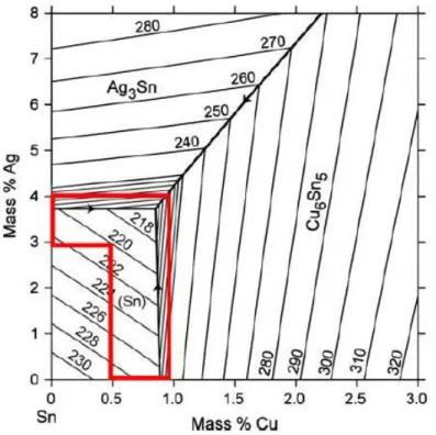
In Figure 2.11, is shown the Sn-Ag-Cu ternary phase diagram near the tin corner. This area in the red box is the near eutectic region. Most of the SAC alloys compositions presently in the market are in this region [11].
Figure 2.11The ternary phase diagram of Sn-Ag-Cu alloys [11].
The types of IMCs formed depends on the surface finish type used in the PCB substrate. Table 2.2 shows the different intermetallic compounds between SAC alloy and various substrates.
Table 2.2 Different IMCs formed between SAC alloy and substrates [2, 30].
Substrates IMCs
Imm.Sn Cu3Sn; Cu6Sn5
LFHASL Cu3Sn; Cu6Sn5
OSP Cu3Sn; Cu6Sn5
ENIG (Cu, Ni)6Sn5; (Cu, Ni, Au)6Sn3
The composition of the IMC layer formed on bare copper and on copper coated with immersion tin, lead-free HASL and OSP are basically the same [31]. If the pads (Cu) are protected with an ENIG coating, the Au dissolves and migrates into the solder, promoting the intermetallic layer formation between the liquid solder elements (Sn, Cu...) and Ni.
The thickness of the intermetallic layer should be between 1 and 5 µm [32].
2.6.2. Joint defects
When soldered one electronic product is necessary to know what constitutes a good joint, and how to correct soldering defects.
A defect is a condition that may be insufficient to ensure the form, fit or function of the assembly in its end-use environment. In this sub-section will be presented some common defects that can appear during the assembled process. These defects are present in IPC-A-610E, Acceptability of Electronic Assemblies, where illustrates the requirements for many types of solder connections [33].
The requirements are divided into three classes of acceptance criteria: Class 1 – General electronic products
Includes products suitable for applications where the major requirement is function of the completed electronic assembly;
Class 2 – Dedicated service electronic products
Includes products where continued performance and extended life is required, and for which uninterrupted service is desired but not critical. Typically the end-use environments would not cause failures;
Includes products where continued high performed or performance-on-demand is critical, equipment downtime cannot be tolerated, the end-use environment may be uncommonly harsh, and the equipment must function when required, such as life support or other critical systems [33].
Table 2.3 are presented some common defects in PCBAs:
Table 2.3 Defects which can appear in PCBAs after soldering [33-35].
Defect Description
Solder ball defects
Solder ball defect appears after reflow in form spherical particles with various diameters.
This defect can be caused by the incompatibility between the solder paste and solder resist.
Solder shorts/bridging
This defect appears mostly in wave process in which there is solder connecting between two or more pads before the solder solidifies, creating a short (pads come into contact to form a conductive path).
Poor or incomplete filling
The hole is poorly filled or is not filled completely and the IPC standard states describe that 75% of the hole must be filled. This incomplete filling occurs due to flux and heat issues.
Voids
Voids are classified as spaces within the joint. The contributors for appearing of voids are outgassing of flux entrapped and excessive oxidation.
Tombstoning
A tombstone is a defect characterized by a chip component that has partially or completely lifted off one end of the pad surface.
Solder beading
Solder beading occurs when solder paste gets under of the component softens due to heat input, and flows to the underside of chip components.
3.
C
HAPTER
3
E
XPERIMENTAL
P
ROCEDURES
3.1. Introduction
The starting point of the present work was the study of the inert and oxidant atmosphere influence in the reliability of the solder joint. This thesis includes two different projects which were developed in two institutions: University of Minho (Campus Azurém, Guimarães) and Bosch Car Multimedia (Braga). The present chapter describes the materials, methods, and inspection and characterization techniques. The work performed at the University of Minho included the study of the thermal properties of the solder SAC405. Furthermore, the possibility to solder with an oxidant atmosphere was also analyzed (using SAC305 and SAC405). The second project was developed at a Bosch production line and consisted in the oxidant atmosphere influence study in a real product. The performance of the final product was also evaluated.
3.2. Soldering study with an oxidant atmosphere
In the present project, the main objective consisted in the study and comparison of the intermetallic layer obtained after soldering using different atmospheres, inert and oxidant. The materials that were used in the first project were supplied by Bosch Car Multimedia. The characterization techniques that were used to study the intermetallic layer were the DTA and optical and electronic microscopy.
3.2.1. Materials
Two types of solders SAC305 and SAC405 were used in this project. These are typically used at an industrial scale by Bosch Car Multimedia in the soldering processes. The wave soldering process uses SAC305 and the reflow soldering process implies the use of SAC405. Table 3.1 presents the solders characteristics, such as composition, melting point and density.
Table 3.1 Composition, melting point and density corresponding to SAC305 and SAC405.
Solder Composition (wt. %) Melting point (ºC) Density (g/cm3)
SAC305 96.5Sn-3.0Ag-0.5Cu 217 7.4
SAC405 95.5Sn-4.0Ag-0.5Cu 217-224 7.5
It is important to refer that SAC305 was supplied as solder wire and the SAC405 was supplied as solder paste (with flux).
Regarding the PCB used in the project, this was constituted by a FR4 base, a Cu layer and the surface finish in immersion tin. This PCB presented a thickness of the Cu layer of 35 µm and the thickness of the surface finish of 1.9 µm (Sn).
3.2.2. Methods
This project consisted in the study of the solders properties when an oxidant atmosphere was used during soldering. Therefore, the thermal properties of the solders SAC305 and SAC405 with and without substrate were studied using the DTA technique. The melting and solidification temperatures of the solders were only measured for the solders without substrate.
Regarding the solder/substrate reactivity study, the DTA was also used to study the influence of the atmosphere and temperature on intermetallic layer formation.
3.2.2.1. Solder/substrate reactivity
The study of the intermetallic layer is essential in this study because the IMC layer is responsible for solder joint reliability. Thus, to study the solder/substrate reactivity, the solder alloys used in this project were melted in a resistance furnace (using DTA) under inert and oxidant atmosphere by a constant flow of argon and air, respectively.
A number of tests were made for studying the formation and growth of the intermetallic layer. The experiments were conducted with the two different solders. So, the IMC layer thickness were analyzed at three different temperatures. Table 3.2 present the thermal cycle used in this study. The entire process was conducted under N2 and air atmospheres. A high heating rate (30
ºC/min) was used, in the equipment allowed range, to approach it to the thermal cycle used at Bosch Car Multimedia.
Table 3.2 Thermal cycle used for SAC305 and SAC405.
Solder Thermal cycle
Temperature max. (ºC) Heating rate (ºC/min) Stage (s) Cooling rate (ºC/min)
SAC305 and SAC405 240 30 12 30 250 260 3.2.3. Characterization techniques
3.2.3.1. Differential thermal analyze (DTA)
DTA is a technique in which the difference to a temperature between a sample and a reference material is measured as a function of temperature while the sample and reference are subjected to controlled temperature programmer [36]. The basic principle behind its technique is that when a sample is heated, it undergoes reactions and phase changes that involve absorption or emission of heat.
DTA was used to determine the melting temperature for SAC405 without substrate. Regarding the solders with the substrate, it was also used the DTA for simulation of a cycle thermal. Preparation of the solders without substrate:
SAC405 was supplied in form the solder paste and this was removed from the container and then dropped into aluminum crucibles. The quantity of solder used was approximately 65-80mg. Afterward, the samples were placed in DTA under argon and air atmosphere to induce the melting of the solder. This study was performed only in SAC405.
These tests were performed under different atmospheres, argon and air, and different heating rates. Table 3.3 shows the conditions used in the study. It is important to note that were used the same conditions to different atmospheres.
Table 3.3 Heating-cooling DTA profile used for SAC405.
Solder Thermal cycle
Heating rate (ºC/min) Temperature max. (ºC) Stage (s) Cooling rate (ºC/min)
SAC405
10
260 30 30
20 30
Preparation of the solders with substrate:
In this case, firstly the substrate with a surface finish in immersion tin was prepared. The substrate had approximately 3 mm diameter because the dimensions of the aluminum crucibles were 5 mm diameter. After the preparation of the substrates, flux (no-clean, Cobar 94QMB) was applied in the surface of the substrate and the solder was placed. Samples of the solder SAC305 were cut and polish to obtain a plan surface and follow was placed on the substrate surface. The samples had approximately 65-80 mg each. As the solder SAC405 was removed a few solder of the container and placed on the surface of the substrate. Samples were placed in aluminum crucibles and placed in DTA oven under argon and air atmosphere.
3.2.4. Morphological analysis
The inspection and characterization of the samples can be made through electronic microscopy. In this project the samples had a small size, so for a facility the handling the samples were mounted in resin. The samples were grouped with respect to solder composition for detailed morphological analysis. After the mounting, the samples were subjected to grinding, using a different grip papers with 180, 600 and 1200 mesh. Then, the samples were polished using an abrasive diomond with 6 and 1 µm. To reveal the microstructure the samples were etched using a solution of the ferric chloride (96 ml of the ethyl alcohol more 2 ml of the hydrochloric acid and 5 g of the ferric chloride).
3.2.4.1. Scanning electron microscopy (SEM)
Scanning electron microscopy is a technique for high-resolution imaging of surfaces. The samples were analyzed using a scanning electron microscope to perform a morphological evaluation. SEM micrographs can be found in all Chapter 4.
SEM uses a beam incident of electrons then interact with the atomic structure of the specimen and generate topographic images. Different types of electrons are produced from the beam, secondary and backscattered. The secondary electrons are responsibly by morphology and topography of the samples surfaces and backscattered electrons to achieve phase discrimination. The SEM is also capable of performing analyzes in a specific location using an energy-dispersive X-ray spectroscope (EDS). With the attachment of the EDS, the elemental composition of materials can be determined [37].
A Hitachi TM3030 plus scanning electron microscope was used in this work for characterization of the samples. An accelerating voltage of 15 kV was used to obtain the micrographs at different magnifications.
The microstructural analysis was conducted to quantify and qualify composition of the samples, namely the solder composition and intermetallic layer composition. With the SEM was also measured the interface thickness between the solder and substrate, as shown in Figure 3.1.
3.3. Oxidant atmosphere study in a production line
This sub-section describes the project that was performed in a production line at Bosch Car Multimedia.
The main objective of this project was to study the influence of the oxidant and inert atmosphere in intermetallic formation and evaluation of the solder joint at a Bosch production line.
For this study, was projected a work plan where were defined the steps to perform in the production. For such, this project was divided into two main groups, as shown in the following scheme (Figure 3.2):
Figure 3.2 Schematic representation about the Solar A production.
3.3.1. Materials
In the reflow soldering process was used the solder paste SAC405 which was development by Heraeus® (F620Cu0.5-88M3). Regarding the wave soldering process was used the solder SAC305 which was development by Stannol®. These are the same solders used in the first project, therefore the characteristics are the same (presented in Table 3.1).
Regarding the PCBs used in this project was supplied by Pacific Fame and have the following characteristics:
PCB material: FR4
PCB thickness: 1.6±0.14 mm Cu layer thickness: 39-68 µm Surface finish: Immersion tin Surface finish thickness: 1.0-1.3 µm Panel dimension: 185 x 230 mm PCB dimension: 104 x 135.7 mm
The components used in the soldering process was supplied by Bosch Car Multimedia according to the product specifications.
3.3.2. Methods
For this project was used the product existent at Bosch Car Multimedia. The product produced for this study was a solar panel defined by NSC Solar A. The product was chosen presents a double sided assembly, constituted by surface mount components and through-hole components, and is a lead-free product. Therefore, the production involves two soldering processes: reflow and wave soldering. Surface mount components were reflow soldered to the PCB, followed by wave soldering of the through-hole components and some surface mount components.
The objective of the project was to study the solder joint with different atmospheres in reflow soldering process. Besides, with this project it was possible to study the intermetallic layer formation and growth, in various steps of the production as previously described.
3.3.2.1. Soldering with an inert and oxidant atmosphere
Regarding the thermal profiles, it was used the normal production profile of the NSC Solar A, according to the requirements Bosch Car Multimedia. Table 3.4 presents the soldering data of this product.
Table 3.4 Data about the soldering process, reflow and wave.
Process Alloy Surface finish Flux
Reflow Soldering
In the experimental work, the solder paste was deposited onto the specified upper side volume of the PCB by EKRA X4 professional machine Bosch edition (the stencil printing machine), as represented in Figure 3.3a. The printing was performed by a metal squeegee where the solder paste was pre-applied on a stencil with openings corresponding to the pad on the PCB. The solder paste used in this soldering process was SAC405.
After the solder printing process, in the second step, the components were automatically removed from the transport packaging and mounted in the position provided on the PCB using a Siemens Siplace S20 (pick and place machine) as shown in Figure 3.3b.
After mounting components in solder paste on the side of the PCB, these are soldered by the application of heat in an inert (with nitrogen) and oxidant (air) atmosphere. This way, the reflow oven used in this production was a REHM Inert Gas Reflow Soldering System VXP 3500, as shown in Figure 3.3c.
During the reflow, when using an inert atmosphere, the content of residual oxygen had to be less than 1500 ppm. The PCB was carried on along a conveyor belt system inside of the reflow oven where the transport speed was 0.85 m/min.
The reflow profile used in this production was indicated by Bosch Car Multimedia, and this presented the following stages, heating, soak, and peak and cooling.
Figure 3.3 Reflow process steps: a) EKRA X4 professional machine Bosch edition, b) Siemens Siplace S20, and c) REHM Inert Gas Reflow Soldering System VXP 3500.
This way, the thermal profile used in this production was according to Bosch Car Multimedia requirements. Figure 3.4 shows the reflow profile obtained for the REHM Inert Gas Reflow soldering System VXP 3500.
Stencil printing machine Pick and place machine
Reflow oven
a) b)
![Figure 2.2 Three main categories of printed circuit board: a) single-sided, b) double-sided and c) multi-layered [5]](https://thumb-eu.123doks.com/thumbv2/123dok_br/17613328.820418/25.892.206.732.119.609/figure-categories-printed-circuit-board-single-double-layered.webp)
![Figure 2.7 Typical reflow profile for lead-free Sn-Ag-Cu solder paste [21].](https://thumb-eu.123doks.com/thumbv2/123dok_br/17613328.820418/35.892.178.756.460.857/figure-typical-reflow-profile-lead-free-solder-paste.webp)