(Recebido em 01/03/2011; Texto final em 30/03/2011).
Kinetics of Formation and Growth of Intermetallic Compounds
(Efeito do envelhecimento térmico nas reações interfaciais de ligas de soldagem branda a base de estanho em substratos de cobre e cinética de formação e crescimento de compostos intermetálicos)
J. C. Madeni and S. Liu
Center for Welding, Joining and Coatings Research, Metallurgical & Materials Engineering Department, Colorado School of Mines, U.S.A., [email protected]
ABSTRACT
The formation and growth of intermetallic compounds at the interface between four solder alloys, Sn-3.5Ag, Sn-0.7Cu, Sn-3.2Ag-0.8Cu and Sn-9Zn, and Cu-plated substrates have been studied. Thermal aging tests for 20, 100, 200, 500 hours at 70, 100 and 150 oC were carried out. As expected, results indicate that the formation of the intermetallic layer is a diffusion-controlled process.
Nevertheless, migration and dissolution of Cu into the solder was observed, especially at lower temperatures. The thickness of the layer of intermetallic compound increased with increasing aging temperature and time. The Sn-3.5Ag alloy showed the smallest intermetallic growth and the Sn-9Zn alloy the highest, compared to the other alloys. The results also show deinite morphological differences between the Cu/Cu3Sn, the Cu3Sn/Cu6Sn5 and the Cu6Sn5/solder-matrix interfaces.
Key Words: Tin-based solder alloys, Intermetallic compounds, Isothermal aging, Morphology, Interface, IMC layer growth front.
Resumo: A formação e o crescimento de compostos intermetálicos na interface entre quatro ligas de soldagem branda, Sn-3.5Ag, Sn-0.7Cu, Sn-3.2Ag-0.8Cu e Sn-9Zn e substratos revestidos com Cobre foram estudados. Testes de envelhecimento térmico de 20,
100, 200, 500 horas a 70, 100 e 150 oC, foram realizados. Como esperado, os resultados indicam que a formação da camada de
intermetálicos é um processo controlado por difusão. No entanto, a migração e dissolução de Cu na solda foi observado, especialmente em baixas temperaturas. A espessura da camada de compostos intermetálicos aumentou com o aumento da temperatura e do tempo de envelhecimento. A liga de Sn-3.5Ag apresentou o menor crescimento de intermetálicos e a Sn-9Zn o mais elevado, comparado com as outras ligas. Os resultados também mostram diferenças morfológicas entre as interfaces Cu/Cu3Sn, Cu3Sn/Cu6Sn5 e Cu6Sn5.
Palavras chave: Ligas para soldagem branda a base de estanho, Compostos intermetálicos, Envelhecimento isotérmico, Morfologia, Interface, Frente de crescimento de camada IMC.
1. Introduction
Health and environmental concerns in the electronic packaging industry regarding the use of lead-based alloys led to the search for lead-free substitute alloys. Previous studies have shown that Sn-based alloys such as Sn-3.5Ag, Sn-0.7Cu, Sn-3.2Ag-0.8Cu and Sn-9Zn exhibit promising mechanical properties [1-3] and can be considered as serious candidates to replace the Sn-Pb alloy. Nevertheless, more information is needed before life and reliability predictions can be made for joints using these materials. During relow soldering, a layer of intermetallic compound (IMC) is formed between the substrate and the solder alloy. In solid-state this layer continues to grow and may react to produce additional IMC layers [4]. The concern about these IMCs is that at high operating temperatures they may grow to become detrimental to the mechanical integrity of the solder joints [3,5]. This study provides information about the effects of annealing on the solder/substrate interface
morphology and microstructure. For that purpose, the formation and growth of intermetallic layers between the copper-plated substrates and the Sn-3.5Ag, Sn-0.7Cu, Sn-3.2Ag-0.8Cu and Sn-9Zn alloys is investigated.
2. Experimental Procedure
2.1. Production of copper/solder joints
Effect of Thermal Aging on the Interfacial Reactions of Tin-Based Solder Alloys and Copper Substrates and Kinetics of Formation and Growth of Intermetallic Compounds
any impurities, dirt, and oxide layers present on the surface and promoted wetting. In the case of the Sn-9Zn alloy, a commercial zinc chloride and ammonium chloride based paste was applied to the copper surface, which provided better wetting than the phosphoric acid-based solution applied to the copper substrate for the three previous solder alloys. The solder drops were melted on the substrate at a temperature 50oC above their respective
melting temperatures indicated in Table 1, under argon gas. The joints, with approximately 3mm thick solder, were cooled in air to room temperature.
Table 1. Melting and furnace temperatures for the solder alloys used in this study.
Solder alloy Temperature, (Melting oC)
Furnace Temperature ± 1oC,
(oC)
Sn-3.2Ag-0.8Cu 217 267
Sn-3.5Ag 221 271
Sn-0.7Cu 227 277
Sn-9Zn 198.5 248
2.2. Thermal aging test
The thermal aging tests of the copper/solder joint coupons were done using furnaces with temperatures controlled to ± 1oC. To
avoid oxidation during thermal aging, a continuous low of industrial grade argon gas was provided to the furnaces. The copper/solder joints were thermally aged at 70, 100 and 150 oC,
and for 20, 100, 200 and 500 hours. The specimens were water-quenched as they were removed from the furnaces.
2.3. Interface characterization
Each sample was cut in half and cold mounted using epoxy for metallographic analysis. The reason for using cold mounting instead of hot mounting is that cold mounting undergoes a lower curing temperature. The mounted samples were ground and polished using standard metallographic techniques, irst to 0.5 mm with diamond slurry, and then to 0.05 mm for 45 minutes using colloidal silica. Polishing the samples in a vibratory machine with colloidal silica resulted in a good etched surface.
The samples were analyzed using light microscopy and scanning electron microscopy (SEM) to characterize the different microstructural features and energy dispersive spectroscopy (EDS) to identify the intermetallic compounds. Quantiication of IMC thickness was done by measuring the linear distance from the edge of the copper substrate to the IMC layer growth front. In the same manner, the measurement of the average total IMC layer thickness when two layers were present was done measuring the linear distance from the edge of the copper substrate to the second IMC layer growth front. Eighty thickness readings along the interface at consistent intervals were averaged
to obtain the average IMC layer thickness for each of the solder alloy-substrate combinations. The IMC thickness measurements were performed using the image analysis software incorporated in the scanning electron microscope.
3. Results And Discussion
3.1. Joint interface characterization
Micrographs of the Cu/Solder alloy interface after soldering, such as the one in Figure 1, indicate the existence of a very small Cu6Sn5 intermetallic layer visible only at high magniications [5,
6]. In the tin/copper and tin-rich-alloys/copper joint systems, the intermetallic Cu6Sn5 (h'-phase) formed immediately upon
contact of the liquid solder with the copper substrate [7, 8]. Then, the intermetallic compound grew rapidly [9,10].
Figure 1. Micrograph of the Cu/Sn-3.5Ag interface after soldering, showing the presence of the Cu6Sn5 intermetallic
layer.
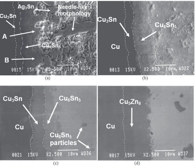
The interface after thermal aging was found to be very different compared to the initial observations immediately following soldering, as shown in Figure 2, in the micrographs of the Cu/Solder interface at 150 oC for 500 hours. Beginning
from the bottom, in Figures 2(a), (b) and (c), the visible layers are the epoxy board, the copper substrate, the intermetallic compounds (IMCs), Cu3Sn and Cu6Sn5, and inally the solder
matrix. It was observed that the layer of Cu3Sn formed at the
Cu/solder interface when the joint was under thermal aging, and the layer of Cu6Sn5 resulted on top of Cu3Sn. This sequence is
true for the three solder alloy systems, Cu/Sn-3.2Ag-0.8Cu, Cu/ Sn-3.5Ag, and Cu/Sn-0.7Cu. In the case of Cu/Sn-3.5Ag, a few small particles of Ag3Sn can also be observed along the Cu6Sn5/
Sn-3.5Ag interface. Different from the previous joint systems, the Cu/Sn-9Zn system displayed only one intermetallic layer, Cu5Zn8 as evidenced in Figure 2(d).
3.2. Identiication of the intermetallic compounds
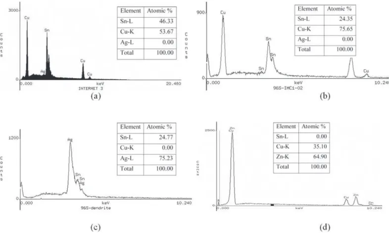
Energy dispersive spectroscopy (EDS) analysis was used to identify the intermetallic compounds present in each of the joint samples. The characteristic x-ray intensity spectrum and the chemical data Sn = 46.33 at. pct. and Cu = 53.67 at. pct. (close to the 6:5 Cu/Sn molar ratio) in Figure 3(a) clearly show intensity peaks corresponding to the h'-phase in the copper-tin phase diagram (included as Appendix A), which is the Cu6Sn5
intermetallic compound. This IMC is present in the as-soldered and annealed samples.
Similarly the data in Figure 3(b) was analyzed. The high Cu and lower Sn x-ray intensity peaks indicate that copper is the major component of the compound. The chemical composition, Sn = 24.35 at. pct. and Cu = 75.65 at. pct., which is close to the 3:1 molar ratio of Cu/Sn, approaches the stoichiometric composition of Cu3Sn. Using the atomic percent of the two
Appendix A, the compound falls inside the e-phase region, which indeed is the Cu3Sn intermetallic. The EDS spectrum in
Figure 3(c) was obtained from area “A” in the micrograph in Figure 2(a), which indicates higher number of counts (peaks) of silver compared to those of tin. The data points indicate Sn and Ag in the amounts of 24.77 at. pct. and 75.23 at. pct., respectively. Locating these atomic percents on the tin-silver phase diagram in Appendix B, the intermetallic compound can be determined as Ag3Sn (g-phase).
The EDS spectrum in Figure 3(d) indicates the presence of two elements, copper and zinc; the larger number of zinc peaks suggest higher amounts of zinc. Indeed, the atomic percent of copper and zinc, 35.10 at. pct. and 64.90 at. pct., respectively, conirm the existence of more zinc in the compound. Locating these amounts of copper and zinc on the copper-zinc phase
diagram shown in Appendix C, it is found that the intermetallic is the Cu5Zn8 (g-phase). The intermetallic compounds identiied
in this study are in agreement with previous reports made by J.Y. Park et al. [11], and C. Hang et al. [12].
3.3. Morphology of the intermetallic layers
Evidence of interface morphological differences was found between the IMCs. The Cu3Sn/Cu6Sn5 interface was
observed to be irregular [11-13]. The thickness variation of the Cu3Sn intermetallic layer was not as drastic as the thickness
of the Cu6Sn5 intermetallic layer. In the case of the Cu6Sn5/
solder-matrix, the interface is more irregular, with localized developments of elongated, needle-like, or elongated scalloped structures [14,15], growing far into the solder matrix. According Figure 2. Micrographs of the Cu/solder interfaces at 150oC for 500 hours, for the four solder alloy systems, indicating their respective
Effect of Thermal Aging on the Interfacial Reactions of Tin-Based Solder Alloys and Copper Substrates and Kinetics of Formation and Growth of Intermetallic Compounds
to Y.G. Lee et al. [6] the irregularity of the solder/IMC interface takes place during a liquid-solid reaction during soldering.
Cu/Sn-3.5Ag System
In the case of the Cu/Sn-3.5Ag system, the morphology of the Cu6Sn5 layer is signiicantly different from that of Cu3Sn. Figure 4(a) clearly exhibits the irregular interface of the Cu6Sn5 intermetallic, protruding into the solder matrix. Some areas of this interface (growth front) developed into elongated, needle-like morphologies such as the one shown in the micrograph. In other areas, the initiation of the needle-like morphologies, “A”, and the formation of the scalloped structures [16], “B”, were observed, Figure 4(a). In addition, Ag3Sn was found in the form of small particles at the Cu6Sn5/solder interface. It is plausible that these small particles of Ag3Sn interrupted the fast growth of the Cu6Sn5 layer. The growth front of the Cu3Sn layer is not as irregular as that of the Cu6Sn5. For better visual clariication of the micrograph in Figure 4(a), the Cu3Sn growth front has been outlined with a dash-dotted line, and the copper surface with a dashed line. It seems that the irregularity of the Cu3Sn layer depended more on the original surface of the copper substrate.
Cu/Sn-3.2Ag-0.8Cu System and Cu/Sn-0.7Cu System
In the case of the Cu/Sn-3.2Ag-0.8Cu and Cu/Sn-0.7Cu, the interface of the Cu6Sn5 is smoother than that observed in the Cu/
Figure 3. EDS spectrum identifying the intermetallic compounds at the Cu/solder interface. (a) Cu6Sn5, (b) Cu3Sn, (c) Ag3Sn, (d)
Cu5Zn8.
Sn-3.5Ag system. Evidence of this observation can be found in Figures 4(b) and (c). Figure 4(b) displays the Cu/Sn-3.2Ag-0.8Cu interface. The most noticeable feature of this interface is that the Cu6Sn5 growth front was irregular but did not have sharp features as in the previous case of Cu/Sn-3.5Ag. For example, the needle-like and scalloped structures are not present here. The Cu3Sn growth front was also irregular.
In the case of the Cu/Sn-0.7Cu interface shown in Figure 4(c), the irregularity of the Cu6Sn5 growth front was more than in the case of the Cu/Sn-3.2Ag-0.8Cu. This interface also exhibited small pieces of Cu6Sn5 (~1 to 2 microns in size) detached from the Cu6Sn5 layer, but they did not seem to grow far into the solder matrix. Again, the Cu3Sn growth front exhibited irregular characteristics.
Cu/Sn-9Zn System
3.4. Kinetics of intermetallic layer growth
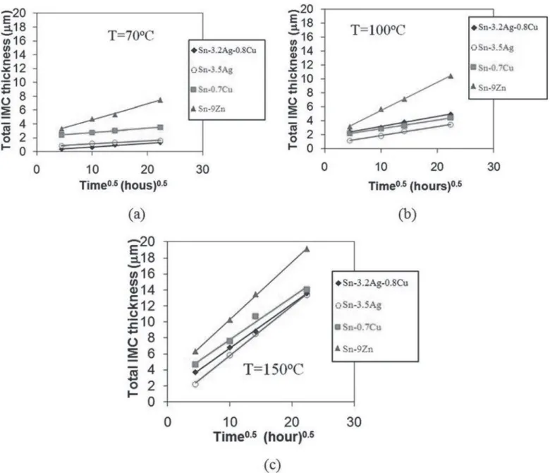
The growth kinetics of the IMCs as a function of aging time and temperature was analyzed by evaluating the thicknesses of the IMC layers. The method of determining the IMC thickness was presented in the experimental section of this document. The thicknesses of individual Cu3Sn and Cu6Sn5 layers and combined (Cu3Sn + Cu6Sn5) IMC layers were measured. The total intermetallic layer thickness measured in the four material systems at 150oC, the highest aging temperature used
in the experiments, and for 500 hours were determined in the following: 13.3 mm for 3.5Ag, 13.6 mm for Cu/Sn-3.2Ag-0.8Cu, 14.1 mm for Cu/Sn-0.7 Cu, and 19.1 mm for the Cu/Sn-9Zn alloy.
Figure 4 (a) Cu/Sn-3.5Ag interface exhibiting the irregularity of the Cu3Sn and Cu6Sn5 intermetallics growth front and the Ag3Sn
scalloped and needle-like morphologies. (b) Secondary electron image of the Cu/Sn-3.2Ag-0.8Cu interface, and (c) Backscattered electron image of the Cu/Sn-0.7Cu interface, and (d) Backscattered electron image of the Cu/Sn-9Zn interface.
A simple parabolic, diffusion-controlled growth model, represented by equation (1), was assumed in the analysis of these experiments.
X = (kt)
1/2 (1)X is the thickness of the intermetallic layer, k is the growth constant, and t the time. The observed total IMC thickness and time relationships at 70, 100 and 150 oC, shown in Figures
5(a), (b) and (c) respectively, were found to obey the parabolic relationship assumed previously. Other researchers such as Vianco et al.17 and Lee et al.6 have found similar relationships.
Effect of Thermal Aging on the Interfacial Reactions of Tin-Based Solder Alloys and Copper Substrates and Kinetics of Formation and Growth of Intermetallic Compounds
growth; therefore, as the temperature increased, the rate of IMC layer growth increased. At the three temperatures, the Sn-9Zn alloy grew at the fastest rate. The Sn-3.5Ag alloy grew at the slowest rate at 70 and 100 oC, and the Sn-3.2Ag-0.8Cu alloy at
150 oC.
Similar analysis was conducted for each of the individual IMCs in each Cu/solder system. The general observation is that their growth also obeyed the parabolic growth as in the case of the growth of the total IMC. Figure 6 shows how the individual IMCs grew with time.
In the case of the Cu/Sn-3.2Ag-0.8Cu joint system, shown in Figure 6(a), the growth rate of the two intermetallic compounds, Cu6Sn5 and Cu3Sn, are statistically similar. In the case of the
Cu/Sn-3.5Ag system, shown in Figure 6(b), the Cu6Sn5 layer
grew at a faster rate than the Cu3Sn layer. This observed trend
can be explained as since abundant tin atoms are available they
Figure 5. Total IMC growth (Cu3Sn + Cu6Sn5) at the Cu/solder interface at three temperatures, (a) 70 oC, (b) 100 oC, and (c) 150 oC.
irst react with the available copper atoms at the site and form Cu6Sn5. Cu3Sn did not grow as fast as in the previous case
because less Sn atoms were available to react with Cu atoms, since Sn would be reacting with Ag to form Ag3Sn at the Cu6Sn5
growth front. The remaining tin atoms at the Cu6Sn5/solder
interface would enhance the diffusion of tin through the Cu6Sn5
intermetallic layer to react with the copper atoms to form the Cu3Sn intermetallic.
In the case of the Cu/Sn-0.7Cu system shown in Figure 6(c), larger amounts of Cu3Sn formed but grew at approximately
the same rate than Cu6Sn5. The Cu3Sn layer grew because no
Ag3Sn were formed in this system. Therefore, more tin atoms
would take part in the diffusion of tin though the Cu6Sn5 layer to
form Cu3Sn. In the case of the Cu/Sn-9Zn system, only Cu5Zn8
formed. Therefore, Cu5Zn8 is considered as the total IMC layer.
formed by the reaction of tin and copper atoms at the solder/ substrate interface and by the diffusion of copper and/or tin atoms through the layer. This IMC process formation is discussed by Vianco et al. [17]. The theory indicated by Flanders et al.[6], states that tin atoms travel towards the copper substrate, irst to form Cu6Sn5 and then through the Cu6Sn5 layer to form Cu3Sn.
However, if that would be the case, the activation energy for the formation of Cu6Sn5 would have been lower but it is not, as
is shown in Table 2. It should be noted that at lower activation energies the reaction would proceed easier than at higher
Figure 6. Individual IMC layers growth for samples aged at 150 oC, (a) Cu/Sn-3.2Ag-0.8Cu, (b) Cu/Sn-3.5Ag, and (c) Cu/Sn-0.7Cu.
activation energies. According to Y.G. Lee et al.[6] and D. Yao et al. [18] there are also different mass transport processes that occur at the solder/substrate interface, such as channels between grains serving as fast diffusion and dissolution paths of Cu in the solder to feed the reaction. However, they also recognize that during aging bulk diffusion is the dominant mechanism of mass transport for the growth of intermetallic compounds. Strong evidence of copper diffusion through the Cu6Sn5 layer to react
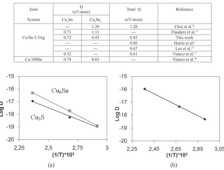
Table 2. Activation energy data for the Cu/Sn-3.5Ag and Cu/100Sn solder systems found in the literature compared to the data for the Cu/Sn-3.5Ag in this work.
Joint (eV/atom)Q Total Q Reference
System Cu3Sn Cu6Sn5 (eV/atom)
--- 1.20 1.20 Choi et al.22
0.73 1.11 --- Flanders et al.13
Cu/Sn-3.5Ag 0.72 0.93 0.85 This work
--- --- 0.80 Harris et al.5
--- --- 0.67 Lee et al.23
0.52 --- 0.61 Vianco et al.17
Cu/100Sn 0.74 0.83 --- Vianco et al.20
Figure 7. Experimental data for the Cu/Sn-3.5Ag system, (a) diffusion data for the individual Cu3Sn and Cu6Sn5 IMCs plotted to
determine the activation energy Q, and (b) diffusion data for the combined IMC (Cu3Sn + Cu6Sn5) plotted to determine the activation
energy Q, for the combined IMC growth.
The constant k in Equation (1) was determined from the slopes of the lines in the IMC thickness versus time0.5 plots,
Figure 5. Using the Arrhenius equation below,
(2)
where ko is the pre-exponential term, Q the activation energy,
R the Universal Gas Constant and T, the absolute temperature. The log k versus (1/T) plots for the individual phases and for the total IMC can be made. Both Figures 7(a) and (b) are for the Cu/ Sn-3.5Ag system. The slopes of the lines in Figure 7(a) suggest higher activation energy for Cu6Sn5 formation than for Cu3Sn.
The line in Figure 7(b) corresponds to the combination of the two intermetallic phases in one layer. As expected, its slope suggests intermediate activation energy value.
The activation energies, Q, were calculated from the slope of the Arrhenius plot using a linear regression model. As the activation energy of a speciic intermetallic compound increases, the formation and growth of this compound is expected to be more dificult. On the other hand, low activation energies indicate easier IMC formation and growth. The results of the activation energies for the total IMC thickness and for the individual phases for the four solder alloys are presented in Table 3. The activation energy data for the Cu/Sn-3.5Ag and Cu/Sn-0.7Cu joint systems are in good agreement with previous studies found in the literature [3,8]. In the case of the Cu/Sn-3.2Ag-0.8Cu and Cu/Sn-9Zn joint systems, no comparison data were found in the literature.
Table 3. Activation energies, Q, determined experimentally for the total (combined) and individual IMCs in the Cu/Sn-3.8Ag-0.8Cu, Cu/Sn-3.5Ag, Cu/Sn-0.7Cu, and Cu/Sn-9Zn joint
systems.
ALLOY IMC Q (kJ/mol) Q (eV/atom)
Sn-3.2Ag-0.8Cu Total 70.9 0.74
Cu3Sn 69.2 0.72
Cu6Sn5 72.2 0.75
Sn-3.5Ag Total 81.6 0.85
Cu3Sn 69.2 0.72
Cu6Sn5 90.0 0.93
Sn-0.7Cu Total 65.5 0.68
Cu3Sn 59.2 0.61
Cu6Sn5 72.2 0.75
Sn-9Zn Cu5Zn8 33.8 0.35
As discussed earlier, data for the Cu/Sn-3.5Ag were collected from the literature [18,20-24] and reported in Table 2. Data obtained in this work were also included in the table for comparison. In this work the activation energies determined for the individual intermetallic compounds, Cu3Sn and Cu6Sn5,
are 0.72 and 0.93 eV/atom, respectively. Table 3 shows that Flanders et al. have obtained almost similar activation energy for Cu3Sn (0.73 eV/atom) and much higher for Cu6Sn5 (1.11 eV/
atom). The value of 0.8 eV/atom for the total activation energy reported by Harris agrees with the 0.85 eV/atom obtained in this work. Nevertheless, the values reported by Vianco et al. of 0.52 eV/atom for the Cu3Sn IMC and 0.61 eV/atom for the
total IMC are lower than all the data in table 3. This difference may be due to the different processes utilized in the production of the joint specimens. It is shown by Lee et al.6 that furnace
heating soldering process would produce higher amounts of IMCs than hot dipped and electroplating, in that order. Vianco [20] reported the behavior of IMCs in Sn-rich solder alloys in an electronic joint. Table 3 shows that the activation energies for this system are 0.74 eV/atom for the Cu3Sn IMC and 0.83 eV/
atom for the Cu6Sn5 IMC. These data is in close agreement with
the data obtained in this work.
4. CONCLUSIONS
Two intermetallic compounds Cu3Sn and Cu6Sn5, form
at the Cu/Sn-3.5Ag, Cu/Sn-3.2Ag-0.8Cu, and Cu/Sn-0.7 Cu interfaces. In the case of the Cu/Sn-9Zn system, the IMC is Cu5Zn8. The three intermetallic layers grew by thermal
activation in a parabolic manner. If IMC formation were the sole criterion for determination of candidates for replacing the Sn-Pb alloys, the ranking would be: 3.5Ag, 3.2Ag-0.8Cu, Sn-0.7Cu and Sn-9Zn, being Sn-3.5Ag the system that exhibited the least IMC growth. The Sn-3.5Ag system also reported the highest activation energy to promote combined IMC formation, 0.85 eV/atom.
5. ACKNOWLEDGEMENTS
The authors would like to thank the National Institute of Standards and Technology (NIST) for their support.
6. REFERENCES
[1] N.C. Lee, Soldering Surf. Mount Technol. 26, 65 (1997) [2] M. Abtew and G. Selvaduray, Mater. Sci. Eng. 27, 95 (2000) [3] J. Madeni, S, Liu, T. Siewert, ASM International - TMS Annual Conference, Indianapolis, Conference Proceedings (2001) [4] Westbrook, J.H. (Ed.), “Intermetallic compounds”, John Wiley & Sons Ltd. 1967, New York, NY and Chichester. [5] P. G. Harris and K. S. Chaggar, Soldering Surf. Mount Technol. 10/3, (1998), pp. 38-52
[6] Y.G. Lee and J.G. Duh, J. Mater. Sci.: Materials in Electronics
10 (1999), 33-43
[7] F. Bartels, J.W. Morris, Jr., G. Dalke, and W. Gust, J. Electron. Mater. 23, 787, (1994)
[8] S. Bader, W. Gust, and H. Heiber, Acta Metall. Mater. 43, 329 (1995)
[9] H.K. Kim, H.K. Liou, and K.N. Tu, Appl. Phys. Lett. 66, 2337 (1995)
[10] A. Hayashi, C.R. Kao, and Y.A. Chang, Scripta Metall. 37, 393 (1997)
[11] Jae-Yong Park, Choong-Un Kim, Ted Carper and Viswana-dham Puligandla, J. Electron. Mater. Vol. 32, No. 11, (2003) [12] Chi-Won Hang, Keun-Soo Kim and Katsuaki Suganuma, J. Electron. Mater. Vol. 32, No. 11, (2003)
[13] D.R. Flanders, E.G. Jacobs and R.F. Pinizzotto, J. Electron. Mater. Col. 26, No. 7, (1997)
[14] Jong-Hyun Lee and Yong-Seog Kim, J. Electron. Mater.
Vol. 31, No. 6, (2002), pp. 576-583
[15] R.A. Gagliano, G. Ghosh, and M.E. Fine, J. Electron. Mater. Vol. 31, No.11, (2002), pp. 1195-1202
[16] T.H. Chuang, H.M. Wu, M.D. Cheng, S.Y. Chang, and S.F. Yen, J. Electron. Mater. Vol. 33, No.1, (2004), pp. 22-27 [17] P. T. Vianco, A. C. Kilgo, R. Grant, “Intermetallic compound layer growth kinetics in non lead bearing solders”, Sandia National Laboratories, Albuquerque, NM, 1995.
[18] S. D. Yao and J. K. Shang, IEEE Trans Complex Hybrids Manuf. Technol. B, 19 (1996) 154.
[19] S.J. Wang and C.Y. Liu, J. Electron. Mater. Vol. 32, No. 11, (2003), pp. 1303-1309
[20] P. T. Vianco, P. L. Hopkins, K.L. Erikson, D. R. Frear, and R. Davidson, Design and Reliability of Solders and solder Interconnections, The Minerals, Metals and Materials Society, (1997) pp. 161-170.
[21] Kithva H. Prakash and Thirumany Srithatan, J. Electron. Mater. Vol. 32, No. 9, (2003), pp. 939-947.
[22] S. Choi, T.R. Bieler, J.P. Lucas and K.N. Subramanian, J. Electron. Mater. 28, 1209 (1999)
[22] C.B. Lee, S.J. Suh, Y.E. Shin, C.C. Shur, and S.B. Jung, Proc. 8th
APPENDIX – A
APPENDIX – B
APPENDIX – C