UNIVERSIDADE DO ALGARVE
INSTITUTO SUPERIOR DE ENGENHARIA
A
GING
S
ENSOR FOR
CMOS
M
EMORY
C
ELLS
S
ENSOR DEE
NVELHECIMENTO PARAC
ÉLULAS DEM
EMÓRIACMOS
Hugo Fernandes da Silva Santos
Thesis to obtain the Master of Science Degree in Electrical and Electronics Engineering
Specialization in Information Technologies and Telecommunications
Tutor: Professor Doutor Jorge Filipe Leal Costa Semião
Title: Aging Sensor for CMOS Memory Cells
Authorship: Hugo Fernandes da Silva Santos
I hereby declare to be the author of this original and unique work. Authors and references in use are properly cited in the text and are all listed in the reference section.
_________________________________ Hugo Fernandes da Silva Santos
Copyright © 2015. All rights reserved to Hugo Fernandes da Silva Santos. University of Algarve owns the perpetual, without geographical boundaries, right to archive and publicize this work through printed copies reproduced on paper or digital form, or by any other media currently known or hereafter invented, to promote it through scientific repositories and admit its copy and distribution for educational and research, non-commercial, purposes, as long as credit is given to the author and publisher.
Copyright © 2015. Todos os direitos reservados em nome de Hugo Fernandes da Silva Santos. A Universidade do Algarve tem o direito, perpétuo e sem limites geográficos, de arquivar e publicitar este trabalho através de exemplares impressos reproduzidos em papel ou de forma digital, ou por qualquer outro meio conhecido ou que venha a ser inventado, de o divulgar através de repositórios científicos e de admitir a sua cópia e distribuição com objetivos educacionais ou de investigação, não comerciais, desde que seja dado crédito ao autor e editor.
A
CKNOWLEDGMENTSFirstly, I would like to express my sincere gratitude to my tutor Professor Jorge Semião, for all the support, guidelines and motivation during the elaboration of this dissertation. With his knowledge and ideas in microelectronics and many other areas of engineering, Professor taught me since my first day in the course, how easy is to approach and solve an engineering or even a life problem. Thank you Professor.
I thank to all my course mates and friends for the long hours of study, patience, shared knowledge and uninterrupted words and examples of motivation. João Duarte, Mário Saleiro, Micael Martins, David Saraiva, Francisco Costa, Vera Alves and eLab Hackerspace team, thank you for everything.
Finally I thank my dear family, in special to my father and to my mother for the never ending motivation and help to pursuit my objectives.
R
ESUMOAs memórias Complementary Metal Oxide Semiconductor (CMOS) ocupam uma percentagem de área significativa nos circuitos integrados e, com o desenvolvimento de tecnologias de fabrico a uma escala cada vez mais reduzida, surgem problemas de performance e de fiabilidade. Efeitos como o BTI (Bias Thermal Instability), TDDB (Time
Dependent Dielectric Breakdown), HCI (Hot Carrier Injection), EM (Electromigration),
degradam os parâmetros físicos dos transístores de efeito de campo (MOSFET), alterando as suas propriedades elétricas ao longo do tempo. O efeito BTI pode ser subdividido em NBTI (Negative BTI) e PBTI (Positive BTI). O efeito NBTI é dominante no processo de degradação e envelhecimento dos transístores CMOS, afetando os transístores PMOS, enquanto o efeito PBTI assume especial relevância na degradação dos transístores NMOS. A degradação provocada por estes efeitos, manifesta-se nos transístores através do incremento do módulo da tensão de limiar de condução |𝑉𝑡ℎ| ao longo do tempo. A degradação dos transístores é designada por envelhecimento, sendo estes efeitos cumulativos e possuindo um grande impacto na performance do circuito, em particular se ocorrerem outras variações paramétricas. Outras variações paramétricas adicionais que podem ocorrer são as variações de processo (P), tensão (V) e temperatura (T), ou considerando todas estas variações, e de uma forma genérica, PVTA (Process, Voltage, Temperature and Aging).
As células de memória de acesso aleatório (RAM, Random Access Memory), em particular as memórias estáticas (SRAM, Static Random Access Memory) e dinâmicas (DRAM, Dynamic Random Access Memory), possuem tempos de leitura e escrita precisos. Quando ao longo do tempo ocorre o envelhecimento das células de memória, devido à degradação das propriedades dos transístores MOSFET, ocorre também uma degradação da performance das células de memória. A degradação de performance é, portanto, resultado das transições lentas que ocorrem, devido ao envelhecimento dos transístores MOSFET que comutam mais tarde, comparativamente a transístores novos. A degradação de performance nas memórias devido às transições lentas pode traduzir-se em leituras e escritas mais lentas, bem como em alterações na capacidade de armazenamento da memória. Esta propriedade pode ser expressa através da margem de sinal ruído (SNM). O SNM é reduzido com o envelhecimento dos transístores MOSFET e, quando o valor do SNM é baixo, a célula perde
a sua capacidade de armazenamento, tornando-se mais vulnerável a fontes de ruído. O SNM é, portanto, um valor que permite efetuar a aferição (benchmarking) e comparar as características da memória perante o envelhecimento ou outras variações paramétricas que possam ocorrer. O envelhecimento das memórias CMOS traduz-se portanto na ocorrência de erros nas memórias ao longo do tempo, o que é indesejável especialmente em sistemas críticos.
O trabalho apresentado nesta dissertação tem como objetivo o desenvolvimento de um sensor de envelhecimento e performance para memórias CMOS, detetando e sinalizando para o exterior o envelhecimento em células de memória SRAM devido à constante monitorização da sua performance. O sensor de envelhecimento e performance é ligado na
bit line da célula de memória e monitoriza ativamente as operações de leitura e escrita
decorrentes da operação da memória.
O sensor de envelhecimento é composto por dois blocos: um detetor de transições e um detetor de pulsos. O detetor de transições é constituído por oito inversores e uma porta lógica XOR realizada com portas de passagem. Os inversores possuem diferentes relações nos tamanhos dos transístores P/N, permitindo tempos de comutação em diferentes valores de tensão. Assim, quando os inversores com tensões de comutações diferentes são estimulados pelo mesmo sinal de entrada e são ligados a uma porta XOR, permitem gerar na saída um impulso sempre que existe uma comutação na bit line. O impulso terá, portanto, uma duração proporcional ao tempo de comutação do sinal de entrada, que neste caso particular são as operações de leitura e escrita da memória. Quando o envelhecimento ocorre e as transições se tornam mais lentas, os pulsos possuem uma duração superior face aos pulsos gerados numa SRAM nova. Os pulsos gerados seguem para um elemento de atraso (delay
element) que provoca um atraso aos pulsos, invertendo-os de seguida, e garantindo que a
duração dos pulsos é suficiente para que exista uma deteção. O impulso gerado é ligado ao bloco seguinte que compõe o sensor de envelhecimento e performance, sendo um circuito detetor de pulso.
O detetor de pulso implementa um NOR CMOS, controlado por um sinal de relógio (clock) e pelos pulsos invertidos. Quando os dois sinais de input do NOR são ‘0’ o output resultante será ‘1’, criando desta forma uma janela de deteção. O sensor de envelhecimento será ajustado em cada implementação, de forma a que numa célula de memória nova os pulsos invertidos se encontrem alinhados temporalmente com os pulsos de relógio. Este ajuste é feito durante a fase de projeto, em função da frequência de operação requerida para a
definição do período do sinal de relógio. À medida que o envelhecimento dos circuitos ocorre e as comutações nos transístores se tornam mais lentas, a duração dos pulsos aumenta e consequentemente entram na janela de deteção, originando uma sinalização na saída do sensor. Assim, caso ocorram operações de leitura e escrita instáveis, ou seja, que apresentem tempos de execução acima do expectável ou que os seus níveis lógicos estejam degradados, o sensor de envelhecimento e performance devolve para o exterior ‘1’, sinalizando um desempenho crítico para a operação realizada, caso contrário a saída será ‘0’, indicando que não é verificado nenhum erro no desempenho das operações de escrita e leitura.
Os transístores do sensor de envelhecimento e performance são dimensionados de acordo com a implementação; por exemplo, os modelos dos transístores selecionados, tensões de alimentação, ou número de células de memória conectadas na bit line, influenciam o dimensionamento prévio do sensor, já que tanto a performance da memória como o desempenho do sensor dependem das condições de operação.
Outras soluções previamente propostas e disponíveis na literatura, nomeadamente o sensor de envelhecimento embebido no circuito OCAS (On-Chip Aging Sensor), permitem detetar envelhecimento numa SRAM devido ao envelhecimento por NBTI. Porém esta solução OCAS apenas se aplica a um conjunto de células SRAM conectadas a uma bit line, não sendo aplicado individualmente a outras células de memória como uma DRAM e não contemplando o efeito PBTI.
Uma outra solução já existente, o sensor Scout flip-flop utilizado para aplicações ASIC (Application Specific Integrated Circuit) em circuitos digitais síncronos, atua também como um sensor de performance local e responde de forma preditiva na monitorização de faltas por atraso, utilizando por base janelas de deteção. Esta solução não foi projetada para a monitorização de operações de leitura e escrita em memórias SRAM e DRAM. No entanto, pela sua forma de atuar, esta solução aproxima-se mais da solução proposta neste trabalho, uma vez que o seu funcionamento se baseia em sinalização de sinais atrasados.
Nesta dissertação, o recurso a simulações SPICE (Simulation Program with Integrated Circuit Emphasis) permite validar e testar o sensor de envelhecimento e performance. O caso de estudo utilizado para aplicar o sensor é uma memória CMOS, SRAM, composta por 6 transístores, juntamente com os seus circuitos periféricos, nomeadamente o amplificador sensor e o circuito de pré-carga e equalização, desenvolvidos em tecnologia CMOS de 65nm e 22nm, com recurso aos modelos de MOSFET ”Berkeley Predictive Technology Models (PTM)”. O sensor é devolvido e testado em 65nm e em 22nm com os modelos PTM, permitindo caracterizar o sensor de envelhecimento e performance desenvolvido, avaliando
também de que forma o envelhecimento degrada as operações de leitura e escrita da SRAM, bem como a sua capacidade de armazenamento e robustez face ao ruído.
Por fim, as simulações apresentadas provam que o sensor de envelhecimento e performance desenvolvido nesta tese de mestrado permite monitorizar com sucesso a performance e o envelhecimento de circuitos de memória SRAM, ultrapassando os desafios existentes nas anteriores soluções disponíveis para envelhecimento de memórias. Verificou-se que na preVerificou-sença de um envelhecimento que provoque uma degradação igual ou superior a 10%, o sensor de envelhecimento e performance deteta eficazmente a degradação na performance, sinalizando os erros. A sua utilização em memórias DRAM, embora possível, não foi testada nesta dissertação, ficando reservada para trabalho futuro.
PALAVRAS-CHAVE: Sensor de Envelhecimento e Performance, NBTI, PBTI, SNM, Memórias CMOS, SRAM, Transições Lentas.
A
BSTRACTCMOS memories occupy a significant percentage of the Integrated Circuits footprint. With the development of new manufacturing technologies to a smaller scale, issues about performance and reliability exist. Effects such as BTI (Bias Thermal Instability), TDDB (Time Dependent Dielectric Breakdown), HCI (Hot Carrier Injection), EM (Electromigration), degrade the physical parameters of the CMOS transistors, changing its electrical properties over time. The BTI effect can be subdivided in NBTI (Negative BTI) and PBTI (Positive BTI). The NBTI effect is dominant in the process of degradation and aging of CMOS transistors affecting PMOS transistors, while the PBTI effect is particularly relevant on the NMOS transistors’ degradation. The degradation caused by these effects in the transistors, manifests itself through the increase of |𝑉𝑡ℎ| over the time. The transistors’ degradation is designated by aging, which is cumulative and has a major impact on circuit performance, particularly if there are other parametric variations. Additional parametric variations that can occur are process variations (P), voltage (V) and temperature (T), or considering all these variations, and in a general perspective, PVTA (Process, Voltage, Temperature and Aging).
The work presented in this thesis aims to develop an aging and performance sensor, for CMOS memories, sensing and signaling the aging on SRAM memory cells. The detection strategy consists on the active monitoring of the read and write operations performed by the memory cell on the bit line. In the presence of aging, the memories read and write operations have slower transitions. The slow transitions indicate performance degradations and increase the error occurrence probability, which can't exist in critical systems. Thus, when transitions doesn’t occur during the expected time frame, an error signal is signalized to the output due to a slow transition.
The sensors’ operation is shown using SPICE simulations for 65nm and 22nm technologies, allowing to show their effectiveness on monitoring performance and aging on SRAM memory circuits.
KEYWORDS: Aging and Performance Sensor, NBTI, PBTI, SNM, CMOS Memories, SRAM, Slow Transitions.
C
ONTENTS1. Introduction ... 1
1.1 Problem Analysis ... 2
1.2 Objectives ... 3
1.3 Context of The Research Work ... 4
1.4 Thesis Outline... 5
2. Aging in Memories ... 7
2.1 Aging Effects ... 7
2.1.1 NBTI ... 9
2.1.2 PBTI ... 12
2.2 State of the Art on Aging Sensors ... 13
2.2.1 On-Chip Aging Sensor ... 13
2.2.2 Scout Flip-Flop ... 15
3. CMOS Memory Structure ... 21
3.1 Memory Chip Timing ... 22
3.2 Memory Organization ... 22
3.3 Peripheral Circuits ... 23
3.3.1 Row Address Decoder ... 23
3.3.2 Column Address Decoder ... 24
3.3.3 Precharge and Equalization ... 25
3.4 Sense Amplifier ... 26
3.4.1 Voltage Latch Sense Amplifier ... 26
3.4.2 Current Latch Sense Amplifier ... 28
3.5 SRAM (Static RAM) ... 30
3.5.2 Read Operation ...30
3.5.3 Write Operation ...31
3.6 DRAM (Dynamic RAM) ...33
3.6.1 The DRAM Cell ...33
3.6.2 Read Operation ...34
3.6.3 Write Operation ...34
3.7 Complete Cells ...35
3.7.1 Complete SRAM ...35
3.7.2 Complete DRAM ...36
3.8 SRAM Without Pre-charge ...37
3.9 Static Noise Margin ...39
3.9.1 Concept ...40
3.9.2 Hold Mode and Read Stability ...41
3.9.3 Analytical Derivation of SNM ...43
3.9.4 Simulation Method to Determine SNM ...46
3.9.5 Hold State ...48
3.9.6 Read State ...50
4. Aging and Performance Sensor for CMOS Memory Cells ...53
4.1 Transition Detector ...54
4.1.1 Transition Detector – Implementation 1 ...55
4.1.2 Transition Detector – Implementation 2 ...59
4.1.3 Transition Detector – Implementation 3 ...63
4.2 Pulse Detector ...69
4.2.1 Timer Circuit Implementation ...69
4.2.2 Stability Checker Implementation ...73
4.2.3 NOR-Based Pulse Detector ...80
5. Implementation and Results ... 91
5.1 Layout 1 bit SRAM ... 91
5.1.1 SRAM Cell ... 91
5.1.2 Sense Amplifier ... 92
5.1.3 Pre-charge and Equalizer ... 94
5.1.4 Write Circuitry ... 95
5.1.5 Complete SRAM Cell ... 96
5.2 Aging and Performance Sensor Layout... 97
5.2.1 Transition Detector’s Data Paths ... 98
5.2.2 XOR With Transmission Gates ... 98
5.2.3 Delay Element ... 99
5.2.4 NOR Based Pulse Detector ... 100
5.2.5 Complete Aging and Performance Sensor ... 101
5.3 Results for SRAM with Aging and Performance Sensor ... 102
5.3.1 1 bit SRAM Implementation ... 103
5.3.2 8 bit SRAM Implementation ... 104
5.3.3 64 bit SRAM Implementation ... 107
6. Conclusions and Future Work ... 109
6.1 Conclusions ... 109
6.2 Future Work ... 112
References ... 113
7. Appendix ... 117
L
IST OFF
IGURESFigure 2.1: Schematic of a 6T SRAM cell with NBTI and PBTI [5]. ... 8
Figure 2.2: Graphical representation of the SNM degradation for 6T-SRAM [13]. ... 8
Figure 2.3: Si-SiO2 interface in 2-D along with the Si-H bonds and the interface traps. Dit is the site containing an unsaturated electron (crystal mismatch) leading to the formation of an interface trap [18]. ... 10
Figure 2.4: Dissociation of Si-H bonds by the holes when the PMOS device is biased in inversion and the diffusion of hydrogen into the oxide, thereby generating an interface trap [18]. ... 10
Figure 2.5: Trap generation in periodic stress and relaxation against continuous stress [18]. ... 11
Figure 2.6: Illustration of PBTI mechanism (a) stress (b) recovery [5]. ... 12
Figure 2.7: OCAS block diagram [9]. ... 13
Figure 2.8: OCAS schematic [9]. ... 14
Figure 2.9: Local sensor's architecture [10]. ... 15
Figure 2.10: Virtual guard band windows for tolerance and predictive detection of delay-faults in de LS [10]. ... 16
Figure 2.11: Delay element typical architecture: Low delay - DE_L [22]. ... 17
Figure 2.12: Delay element typical architecture: Medium delay - DE_M [22]. ... 18
Figure 2.13: Delay element typical architecture: High delay - DE_H [22]. ... 18
Figure 2.14: Stability checker architecture with on-retention logic [22]. ... 19
Figure 3.1: Memory Access and Cycle Times [26]. ... 22
Figure 3.2: Memory Chip Organized as an Array [23]. ... 23
Figure 3.3: NOR Address Decoder [23]. ... 24
Figure 3.4: Column Decoder [23]. ... 25
Figure 3.5: Precharge and equalizer circuit-DRAM implementation [23]. ... 25
Figure 3.6: Precharge and equalizer circuit-SRAM implementation [23]. ... 26
Figure 3.7: Voltage Latch Sense Amplifier [23]. ... 27
Figure 3.8: DRAM bitline Waveform during the activation of the sense amplifier [23]. . 28
Figure 3.10: CMOS 6T SRAM Memory Cell [23]. ...30
Figure 3.11: SRAM Read Operation Circuit [23]. ...31
Figure 3.12: SRAM Write Operation Circuit [23]. ...32
Figure 3.13: Single Transistor DRAM Cell [23]. ...33
Figure 3.14: Storage Capacitor Connected to Bit Line Capacitance [23]. ...34
Figure 3.15: Complete SRAM Cell [23]. ...35
Figure 3.16:Open Bit Line DRAM Architecture with Dummy Cell [23]. ...37
Figure 3.17: SRAM Non-Precharge [40]. ...38
Figure 3.18: Non Precharge SRAM Waveforms [28]. ...38
Figure 3.19: Block Diagram of a Memory Cell Array [28]. ...39
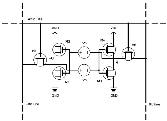
Figure 3.20: A Flip-Flop with static noise sources 𝑽𝒏.[30] ...40
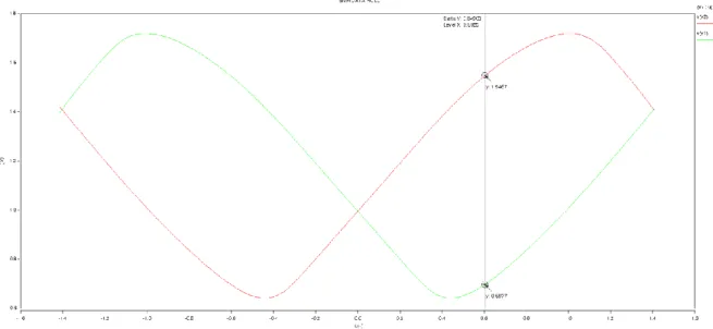
Figure 3.21: Graphical representation of SNM [31]. ...41
Figure 3.22: General SNM characteristics during hold and read operation [34]. ...42
Figure 3.23: SRAM cell during read SNM simulation [30]. ...42
Figure 3.24: SRAM cell with static noise sources 𝑽𝒏 inserted for measuring SNM [30]. ...43
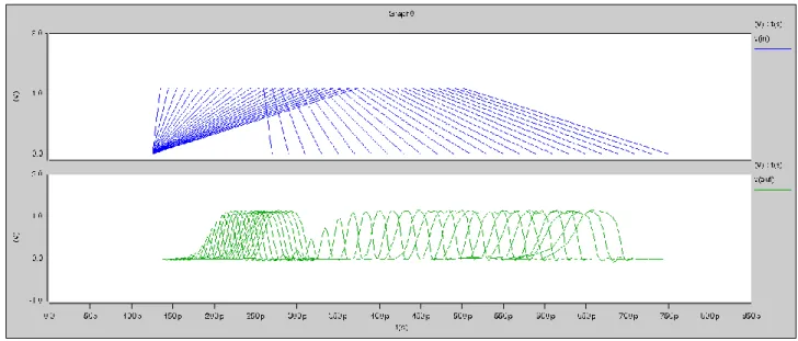
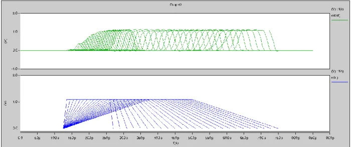
Figure 3.25: SNM estimation in a 45˚ rotated coordinate system [30]. ...46
Figure 3.26: Data hold butterfly curve of a new SRAM. ...49
Figure 3.27: Data hold butterfly curve of an aged SRAM. ...49
Figure 3.28: Data read butterfly curve of a new SRAM. ...50
Figure 3.29: Data read butterfly curve of an aged SRAM. ...51
Figure 4.1: Transitions: a) Fast transition b) Slow transition. ...53
Figure 4.2: Aging and performance sensor block diagram. ...54
Figure 4.3: Transition detector connection block diagram. ...55
Figure 4.4: Transition detector – Implementation 1. ...56
Figure 4.5: Transition detector – Implementation 1, response to input sweep pulse. ...57
Figure 4.6: Transition detector – Implementation 1, response to a single pulse. ...57
Figure 4.7: Transition detector - Implementation 1, response to PVTA variation. ...58
Figure 4.8: Transition detector – Implementation 2. ...59
Figure 4.9: Classic CMOS XOR gate implementation. ...59
Figure 4.10: Transition detector – Implementation 2, response to input sweep pulse. ...61
Figure 4.11: Transition detector – implementation 2, response to a single pulse. ...62
Figure 4.14: Transition detector – Implementation 3. ... 64
Figure 4.15: Transition detector - Implementation 3, response to voltage variation. ... 66
Figure 4.16: Transition detector - Implementation 3, response to temperature variation. . 66
Figure 4.17: Transition detector - Implementation 3, response to 𝑽𝒕𝒉𝒑 variation. ... 67
Figure 4.18: Transition detector - Implementation 3, response to 𝑽𝒕𝒉𝒏 variation. ... 68
Figure 4.19: Timer circuit implementation. ... 70
Figure 4.20: Timer circuit test detection. ... 72
Figure 4.21: Timer circuit, detection with PVTA variations. ... 73
Figure 4.22: Stability-checker implementation. ... 75
Figure 4.23: Pulse detector with Stability-checker operation. ... 75
Figure 4.24: Pulse detector with Stability-checker simulation results. ... 76
Figure 4.25: Pulse detector with Stability-checker simulation results with reduced VDD and increased Temperature. ... 77
Figure 4.26: Pulse detector with Stability-checker simulation results with |Vth| increased in 30%. ... 78
Figure 4.27: Results for complete sensor simulation (transition detector implementation 3 + pulse detector with Stability-checker implementation). ... 79
Figure 4.28: Sensor simulation results (transition detector implementation 3 + pulse detector with Stability-checker implementation) in the presence of VT degradations. ... 79
Figure 4.29: Sensor simulation results (transition detector implementation 3 + pulse detector with Stability-checker implementation) in the presence of Aging degradations. ... 80
Figure 4.30: NOR based pulse detector. ... 81
Figure 4.31: NOR based pulse detector. ... 82
Figure 4.32: NOR based pulse detector, detections test. ... 83
Figure 4.33: NOR based pulse detector, VT variations test. ... 84
Figure 4.34: NOR based pulse detector, Aging variations test. ... 85
Figure 4.35: Sensor simulation results (transition detector implementation 3 + pulse detector with NOR-based implementation) at nominal conditions. ... 86
Figure 4.36: Sensor simulation results (transition detector implementation 3 + pulse detector with NOR-based implementation) in the presence of VT degradations. ... 86
Figure 4.37: Sensor simulation results (transition detector implementation 3 + pulse detector with NOR-based implementation) in the presence of Aging degradations. ... 87
Figure 4.38: Aging and performance sensor schematic. ... 88
Figure 4.40: Aging and performance sensor detection with SRAM 10% aged. ...90 Figure 5.1: SRAM cell layout. ...92 Figure 5.2: Sense amplifier layout. ...93 Figure 5.3: Pre-charge and equalizer layout. ...94 Figure 5.4: Write circuit layout. ...95 Figure 5.5: Complete 1 bit SRAM cell. ...96 Figure 5.6: SRAM read and write cycle. ...97 Figure 5.7: Transition detector layout. ...98 Figure 5.8: XOR with transmission gate. ...99 Figure 5.9: Delay element (DE_H). ...100 Figure 5.10: NOR based pulse detector. ...101 Figure 5.11: Complete aging and performance sensor. ...101 Figure 5.12: Aging and performance sensor simulation. ...102 Figure 5.13: Aging and performance sensor 1 bit SRAM implementation. ...103 Figure 5.14: Aging sensor deployed on a fresh 1bit SRAM cell. ...103 Figure 5.15: Aging sensor deployed on a 10% aged 1bit SRAM cell...104 Figure 5.16: Aging and performance sensor 8 bit SRAM implementation. ...104 Figure 5.17: Write and read on an 8bit SRAM array. ...105 Figure 5.18: Aging and performance sensor on an 8bit SRAM array. ...106 Figure 5.19: Aging and performance sensor on an 8bit SRAM array aged 10%. ...106 Figure 5.20: Aging and performance sensor 64 bit SRAM implementation...107
L
IST OFT
ABLESTable 3.1: Transistor Dimensions [28]. ... 38 Table 4.1: Transition detector – Implementation 1, transistor sizes. ... 56 Table 4.2: Transition detector – Implementation 3, transistor sizes. ... 60 Table 4.3: Transition detector – Implementation 4, transistor sizes. ... 65
L
IST OFA
CRONYMSASIC Application Specific Integrated Circuit
BTI Bias Temperature Instability
CLK Clock
CMOS Complementary Metal-Oxide Semiconductor
CP Critical Path (higher propagation time path)
CUT Circuit Under Test
DE Delay Element
DRAM Dynamic Random-Access Memory
DVFS Dynamic Voltage and Frequency Scaling
DVS Dynamic Voltage Scaling
EM Electromigration
EMI Electromagnetic interference
FET Field-Effect Transistor
FF Flip-flop
Fin-FET Fin Field-Effect Transistor
FPGA Field Programmable Gate Array
H Hydrogen (chemical symbol)
HCA Hot Carrier Aging
HCI Hot Carrier Injection
HK+MG High-K Metal Gate
IC Integrated Circuit
IT Interface Traps
LTD Long Term Degradation
MOSFET Metal-Oxide Semiconductor Field-Effect Transistor
NBTI Negative Bias Temperature Instability
NMOSFET N-type Metal-Oxide Semiconductor Field-Effect Transistor
PBTI Positive Bias Temperature Instability
PMOS P-type Metal-Oxide Semiconductor
PMOSFET P-type Metal-Oxide Semiconductor Field-Effect Transistor
PTM Predictive Technology Model (SPICE transistors models)
PVT Process, power-supply Voltage and Temperature
PVTA Process, power-supply Voltage ,Temperature and Aging
R-D Reaction–Diffusion (model)
Si Silicon (chemical symbol)
SiO2 Silicon Dioxide
SIV Stress Induced Voids
SM Stress Migration
SOI Silicon On Insulator
SPICE Simulation Program with Integrated Circuit Emphasis
SRAM Static Random-Access Memory
T Temperature
TDDB Time Dependent Dielectric Breakdown
V Power-supply Voltage
VT Power-supply Voltage and Temperature
1. I
NTRODUCTIONThe modern integrated circuits are mainly built with Complementary Metal Oxide Semiconductor (CMOS) technology. The manufacturers select this technology to deliver to the world microcontrollers, memories, sensors, transceivers and an endless number of circuits that integrate the modern life devices. Typically CMOS uses complementary and symmetrical pairs of Metal Oxide Semiconductor Field Effect Transistors (MOSFET), p-channel (PMOS) and n-p-channel (NMOS). CMOS technology is widely used worldwide due to low static and power consumption, high switching speed, high density of integration and low cost production.
The most common description of the evolution of CMOS is known as Moore’s law [1]. In 1963 Gordon Moore predicted that as a result of continuous miniaturization, transistor count would double every 18 months. Recently IBM in partnership with Global Foundries announced a 7nm technology chip, the first in the semiconductor industry [2]. The pioneer techniques and fabrication processes, most notably Silicon Germanium (SiGe) channel transistors and Extreme Ultraviolet (EUV) lithography, made this innovative chip possible. The evolution of the fabrication processes and the used technologies, let to predict a future evolution to smaller sizes.
As CMOS technologies continue to scale down to deep sub-micrometer levels, devices are becoming more sensitive to noise sources and other external influences. Systems-on-a-Chip (SoCs) and other integrated circuits, today are composed of nanoscale devices that are crammed in small areas, presenting reliability issues and new challenges. In critical system applications (for example: medical industry, automotive electronics, or aerospace applications), the performance degradation and an eventual failure can’t occur. A system error on this critical applications can lead to the loss of human lives. Thus, time is a key factor in critical-safety systems and, under disturbances, the unexpected increasing of propagation delays may lead to delay faults.
1.1 P
ROBLEMA
NALYSISCMOS circuits’ performance is affected by parametric variations, such as process, power-supply Voltage and Temperature (PVT) [3], as well as aging effects (PVT and Aging – PVTA). The circuit’s aging degradation is pointed to the follow effects: BTI (Bias Temperature Instability), HCI (Hot-Carrier Injection), Electromigration (EM) and TDDB (Time Dependent Dielectric Breakdown) [4]. The most relevant aging effect is the BTI, namely the Negative Bias Temperature Instability (NBTI), which affects mainly the PMOS transistors, resulting in a gradual increase of absolute threshold voltage over time (|𝑉𝑡ℎ𝑝|). As the high-k dielectrics started to be employed from the sub-32nm technologies [5], the BTI also affects significantly the NMOS transistors – Positive Bias Temperature Instability (PBTI), resulting in a rise of the threshold voltage 𝑉𝑡ℎ𝑛 . These effects degrade the circuit’s performance over time, increasing the variability in CMOS circuits, mainly in nanometer technologies. The decrease of performance results in a decrease of switching speed, leading to potential fault delays and consequent chip failures.
Therefore, variability, regardless of their origin, may lead to chip failures [6], especially when several effects occur simultaneously, or when cumulative degradations pile up. Variability also decreases circuit dependability, i.e., its ability to deliver the correct functionality within the specified time frame. Hence, smaller technologies tend to be more susceptible to parametric variations, which lower circuit’s dependability and reliability [7][8]. As a result, the new node SoC chips have: (i) higher performance, but with increased reliability issues; (ii) higher integration, but with increased power densities. These issues place difficult challenges on testing and reliability modelling.
Moreover, today’s Systems-on-Chip (SoC) face the rapidly increasing need to store more information. The increasing need to store more and more information has resulted in the fact that Static Random Access Memories (SRAMs) occupy the greatest part of the System-on-Chip (SoC) silicon area, being currently around 90% of SoC density [9]. Therefore, SRAM’s robustness is considered crucial in order to guarantee the reliability of such SoCs over lifetime [9]. And the trends indicate that this number is still growing in the next years. Consequently, memory has become the main responsible of the overall SoC area, and also for the active and leakage power in embedded systems.
One of the major issues in the design of an SRAM cell is stability. The cell stability determines the sensitivity of the memory to process tolerances and operating conditions. It
write and hold operations. Due to NBTI and PBTI effects, the memory cell aging is accelerated, resulting in degradation of its stability and performance.
Previous works dealing with aging sensors for SRAM cells, especially focused on BTI (Bias Temperature Instability) effect, are attempts to increase reliability in SRAM operation. An example is the On Chip Aging Sensor (OCAS) [9], that detects the aging state of an SRAM array caused by the NBTI effect. With more research work done in this field are the ASIC circuits and applications, and an example is the Scout Flip-Flop sensor [10][11], which acts as a performance sensor for tolerance and predictive detection of delay faults in synchronous circuits. This local sensor creates two distinct guard-band windows: (1) tolerance window, to increase tolerance to late transitions, (2) a detection window, which starts before the clock edge trigger and persists during the tolerance window, to inform that performance and circuit functionality is at risk. However, despite OCAS’ approach to deal with aging in memories, performance sensors for memory applications are still a long way to go, and existing solutions are in an initial stage, when compared to existing ASIC performance sensor solutions.
Consequently, the next years will bring additional challenges that will need to be addressed with new approaches for memory applications dealing with memories’ reliability and power reduction. Therefore, there is a need for R&D work on performance sensors for memories, to deal with Process, power-supply Voltage, Temperature and Aging variations.
1.2 O
BJECTIVESThe main purpose of this work is to develop an Aging and Performance Sensor for CMOS Memory Cells. The proposed aging and performance sensor allows to detect degradation on SRAM memory cells.
The first objective is to design a new sensor for memory applications that can be used in both SRAMs and DRAMs. The new aging sensor will be connected to the memories’ bit lines, to monitor transitions occurred in these signals during read/write operations. The purpose is to show that, by monitoring the bit lines’ operation, it is possible to monitor memory aging and memory’s performance with a very low overhead. The aging and/or performance monitoring is achieved by detecting slow transitions due to a reduction of
performance caused by PVTA variations (or any other effect) in the memory cells or in the memory circuitry (like the sense amplifier, also connected to the bit lines). Besides, by monitoring bit line transitions, the same sensor architecture can be implemented both in SRAM or DRAM memories. Moreover, the underlying principle used when monitoring digital logic aging (as in [10][11]) can be rewardingly reused here to monitor the timing behavior of the memory, or the timing behavior of the bit lines’ transitions.
The second objective is to characterize the aging sensors’ capabilities, creating a SPICE model to implement in the sense amplifier. The simulation environment will submit the circuitry thru aging effects, by shifting the 𝑉𝑡ℎ on the PMOS and NMOS MOSFETs, using Berkeley Predictive Technology Models BPTM 65nm and 22nm transistor models. The test environment will include an SRAM memory cell and all of its peripheral circuitry, namely the sense amplifier, the precharge and the equalizer circuit. The test SRAM cell is a six MOSFET transistors’ cell, and the transistor sizes (namely: (i) the ratio between pull-down and access transistors, (ii) the ratio between pull-up and access transistors (iii) access transistors) were determined to ensure its robustness. To monitor the SRAM degradation, the Static Noise Margin (SNM) will be the used as a metric to benchmark the performance of the SRAM cell before and after aging.
The third objective is to analyze the aging and performance sensor advantages and disadvantages.
If the sensor characteristics analysis reflects a true innovation circuit approach, the fourth and final objective is to submit a patent request for the new sensor for memories.
1.3 C
ONTEXT OFT
HER
ESEARCHW
ORKThe research & development (R&D) work for this Master thesis was conducted at the Superior Institute of Engineering (ISE), University of Algarve (UAlg), in a strict collaboration with the Programmable Systems Lab (PROSYS) of INESC-ID in Lisbon. The work team formed in both Portuguese institutions, has a solid background on aging and performance sensors both for ASIC (Application Specific Integrated Circuit) and for emulated circuits in FPGAs (Field-Programmable Gate Array). This MSc thesis is part of the following research work, which includes also a PhD thesis, to develop new aging aware
sensors and techniques for memories and memory circuitry, and to develop methodologies and tools to reduce power and reliability in memories’ operation.
Finally, the research work developed in this thesis was recently submitted to a definitive Portuguese Patent registration (currently pending), in 29 August, 2015 under the number 108852 C, and entitled to “Performance and Aging Sensor for SRAM and DRAM Memories” [36]. The article for patent submission is presented in the Appendix.
1.4 T
HESISO
UTLINEThis thesis is organized as follows.
In Chapter 2, it is addressed the aging effects that can degrade the circuits performance, particularly the NBTI and PBTI effects. It is also presented the state-of-the-art in aging sensors, namely the on-chip aging sensor OCAS and the Scout Flip-Flop.
Chapter 3 presents the CMOS memory structure, in particular the structure of an SRAM and a DRAM memory cells, peripheral circuits and sense amplifier solutions. It’s also presented the read and write operation of the cells, conducting to the elaboration of memory test circuits to deploy and test the performance and aging sensor. In the end of the chapter it is also presented the Static Noise Margin, working as a benchmark of SRAM cells to analyze its stability.
In Chapter 4 the architecture of the Aging and Performance Sensor for CMOS Memory Cells is presented. The structure is analyzed, and also the schematics and the detection criteria (detection window) which leads the aging sensor to detect slow transitions when circuits aging occurs.
Simulation results are described on Chapter 5, by applying the aging and performance sensor to the memory cell’s bit lines. Parametric simulations using SPICE are also presented, to illustrate how the circuit’s aging affects the cell stability and to prove that the aging sensor detects aging successfully.
Finally, Chapter 6 summarizes the main conclusions of the M.Sc. work, and points out directions for further research.
2. A
GING INM
EMORIESIntegrated circuit aging phenomena has been observed and researched for decades. In the nineties, however, circuit aging became more and more an issue due to the aggressive scaling of the device geometries and the increasing electric fields. At that time, measurements on individual transistors were used to determine circuit design margins, in order to guarantee reliability. After the turn of the century, the introduction of new materials to further scale CMOS technologies introduced additional failure mechanisms and made existing aging effects more severe.
This section reviews the most important integrated-circuit aging phenomena’s, in special the bias temperature instability (BTI) effects: negative bias temperature instability (NBTI) and positive bias temperature instability (PBTI). Since the BTI effects cause the shifting of the threshold voltage, the larger delays also imply lower subthreshold leakage [12].
𝐼𝑠𝑢𝑏 ∝ 𝑒(−𝑉𝑡ℎ) (𝑚𝐾𝑇)⁄ (1)
Consequently, designs are required to build in substantial guardbands in order to guarantee reliable operation over the lifetime of a chip [12]. However, other aging phenomena exist affecting the cells, but in a different scale, such as: hot carrier injection (HCI), time-dependent dielectric breakdown (TDDB) and electromigration (EM).
2.1 A
GINGE
FFECTSOn Figure 2.1 it is shown a 6T SRAM cell with the indication of BTI (NBTI and PBTI). NBTI affects the long-term stability of 6T SRAM cells. In SRAM cells, the threshold voltage shifting over time affects its capability of storing a value. This property is usually compactly expressed in terms of the signal-to-noise margin (SNM): when the SNM becomes
too small, the cell loses its storage capability, hence the SRAM cell suffered an aging induced by NBTI effect [13].
Figure 2.1: Schematic of a 6T SRAM cell with NBTI and PBTI [5].
To characterize the aging effects, a good metric for SRAM aging is given by the Static Noise Margin (SNM) described in detail in section 3.9. The exposure of the cell to aging effects, such as the BTI effect, during years, induces 𝑉𝑡ℎ shifting to the PMOS and NMOS transistors over time, thus moving the static characteristics of the two inverters. From a graphically viewpoint this implies a reduction of the side length of the maximum enclosed square (the darker square in Figure 2.2) [13].
2.1.1 NBTI
The negative bias temperature instability (NBTI), has become a major reliability concern in the present digital circuit designs, affecting the PMOS MOSFETS when stressed with negative gate voltage (𝑉𝑔𝑠=−𝑉𝐷𝐷), leading to a reduction on temporal performance in digital circuits. The NBTI is particularly important below the 130nm technology node, as gate oxide thickness was scaled below 2nm [14]. The effect results in a variation of transistor parameters, for example: threshold voltage (𝑉𝑡ℎ), transconductance (𝐺𝑚), drive current (𝐼𝑑𝑟𝑎𝑖𝑛), etc. [13] [14]. The NBTI effect primarily increases the |𝑉𝑡ℎ𝑃| along the time,
causing a delay fault due to circuit delays [15] [12] [4], [16]–[18]. The amount of threshold voltage degradation of a PMOS transistor due to NBTI depends on several factors (the amount of time elapsed, temperature and voltage profiles experienced by the PMOS transistor, and the workload, which determines the amount of time the PMOS transistor is on), being the voltage threshold shifting the most important parameter to monitor the effect [19]. Formulas (2), (3) and (4) show the proportionality relation of several parameters with the PMOS threshold voltage degradation. On Formula (2), ∆𝑉𝑡ℎ is the PMOS threshold
voltage degradation, 𝑡 is the amount of time, and n=0.25 is typically used for current technologies [18].
∆𝑉𝑡ℎ ∝ 𝑡𝑛 (2)
On formula (3), 𝐸𝑎 is the activation energy of Si, K is the Boltzmann’s constant, and T is
the operating temperature.
∆𝑉𝑡ℎ∝ 𝑒−(𝐸𝑎⁄𝐾𝑇) (3)
On formula (4), 𝑡𝑜𝑥 is the gate oxide thickness, 𝑉𝑔𝑠 is the gate-source voltage and 𝐸0= 2.0 𝑀𝑉/𝑐𝑚.
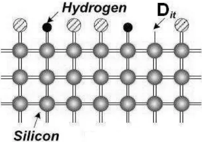
Figure 2.3: Si-SiO2 interface in 2-D along with the Si-H bonds and the interface traps. Dit is the site containing an unsaturated electron (crystal mismatch) leading to the formation of an interface trap [18].
Interface traps (𝐷𝑖𝑡) are formed due to crystal mismatches at the Si-SiO2 interface. During oxidation of Si, most of the tetrahedral Si atoms bond to oxygen. However, some of the atoms bond with hydrogen, leading to the formation of weak Si-H bonds, as seen on Figure 2.3. When a PMOS transistor is biased in inversion, the holes in the channel dissociate these Si-H bonds, thereby generating interface traps (Figure 2.4). Interface traps (interface states) are electrically active physical defects with their energy distributed between the valence and the conduction band in the Si band diagram. They are manifested as an increase in absolute PMOS transistor threshold [14] [18] .
Figure 2.4: Dissociation of Si-H bonds by the holes when the PMOS device is biased in inversion and the diffusion of hydrogen into the oxide, thereby generating an interface trap [18].
While the application of a continuous negative bias to the gate of the PMOS transistor degrades its temporal performance, removal of the bias helps anneal some of the interface traps generated, leading to a partial recovery of the threshold voltage. In Figure 2.5 is shown the generation of traps to continuous stress, and to a periodic stress and relaxation period, and is possible to verify the recovery in number of generated traps in the relaxation period [14] [18].
Figure 2.5: Trap generation in periodic stress and relaxation against continuous stress [18].
The process of degradation and recovery is successfully analyzed using the Reaction-Diffusion (R-D) model [18]. According to the R-D model, the rate of generation of interface traps (𝑁𝐼𝑇) initially depends on the rate of dissociation of the Si-H bonds, which is controlled
by the forward rate constant (𝑘𝑓) and the local self-annealing process which is governed by the rate constant (𝑘𝑟).
𝑁𝐼𝑇= √ 𝑘𝑓𝑁0
𝑘𝑟
(𝐷𝑡)0.25 (5)
The expression (5) results from the derivation of the reaction phase of the R-D model expressions, and the diffusion phase expression, where 𝑁0 is the maximum density of Si-H
states that the generation of interface traps followsa 𝑡𝛼relationship, where α is between 0.17
and 0.3 [18].
2.1.2 PBTI
With the introduction of high-k materials such is 𝐻𝑓𝑂2 (hafnium oxynitride), the degradation effect caused by the positive bias temperature instability (PBTI) started to play an important role on the MOSFET performance [20]. The PBTI effect is more visible on the NMOS transistors for sub-32 nm technologies [5], causing a degradation of the threshold voltage (positive shift), or even voltage threshold instability, particularly to sub-nanometer technologies with the high-k gates, when a positive bias stress is applied across the gate oxide of the NMOS device [12]. This way, SRAM cell requires a more careful design consideration, due to the smaller margin in cell stability, write ability, bit line swing, timing, and also the read access time [5].
The PBTI occurs due to the electron trapping in the high-k layer, presumably due to oxygen vacancies in the layer [21]. Two separate mechanisms are pointed, the filling of preexisting electron traps, and the trap generation, each one dominating at different stress condition regimes. In Figure 2.6 is shown an illustration of PBTI, the trapping phase and de de-trapping or recovery state.
Similarly to NBTI, PBTI effect can be modelled by NMOS 𝑉𝑡ℎ degradations.
2.2 S
TATE OF THEA
RT ONA
GINGS
ENSORSThe SRAM performance and robustness are essential factors to guarantee reliability over the lifetime. The degradation of SRAM cell directly affects the reliability of SoCs. In this context, as already mentioned earlier, one of the most important phenomena that degrades Nano-scale SRAMs reliability is related to Bias Temperature Instability (NBTI and PBTI), which accelerates memory cells aging [9].
To cope with these aging phenomena, several research works have been presented to deal with CMOS circuits’ reliability degradation over time. In this section two of these works are resumed: the first one related with aging sensors for SRAM cells, and the second one related to flip-flop memory cells used in synchronous digital circuits.
2.2.1 ON-CHIP AGING SENSOR
The proposed approach of the on-chip aging sensor (OCAS), consists in detecting the aging state of an SRAM array, caused by the NBTI effect. Connecting one OCAS in every SRAM column, periodically it’s performed an off-line test monitoring the write operation on SRAM and detecting the aging this way. During the idle periods, the sensor is off power, preventing the aging and the power leakage of the OCAS.
In Figure 2.7 and Figure 2.8 is shown the block diagram and the schematic of the proposed OCAS, connected to an SRAM column cell. The transistor TT1 is used to feed the positive bias of the SRAM column and it’s connected between 𝑉𝐷𝐷 and a virtual 𝑉𝐷𝐷 node. The transistors TPG and TNG are switched by power-gating signal and, typically in normal operating mode, they are off, to avoid the aging off OCAS circuitry, and TT1 is on.
During testing mode, the OCAS is powered on, TT1 is switched off and TPG and TNG are connected. Then a write operation is performed on the specific memory cell, which is desired to know the aging state. Meanwhile it’s performed a comparison between the virtual 𝑉𝐷𝐷 node value at the end of the write operation and the reference voltage node. In the end of the process, if the OCAS OUT1 is ‘0’, the SRAM cell is new and fault free. If the value of OUT1 is ‘1’, it’s reported as a fault state and the cell is no more reliable, due to its age state.
The CTRL is set to ‘0’ during the pre-charge phase of the testing mode, and during the evaluation phase this signal is set to ‘1’.
In a general form, the following steps are carried out in order to measure the aging state of a given cell in the SRAM:
1. Select the desired cell's address and read the cell.
2. Change the Testing Mode signal for the column whose cell is to be tested from "0" to "1".
3. Drive the CTRL signal to "0" (Pre-Charge Phase) and write the opposite value as read in step (1).
4. Drive the CTRL signal to "1" (Evaluation Phase) and observe the OCAS’s output for a pass or fail decision.
2.2.2 SCOUT FLIP-FLOP
The Scout Flip-Flop [10] [11] is a performance sensor for tolerance and predictive detection of delay faults in synchronous digital circuits. The Scout FF, constantly observes and inspects the FF data and inform if an unsafe data transition occurs. The unsafe data transitions are identified by the authors as error free data captures in the FF that occur in the eminence (with a pre-defined safety-margin) of a delay error (Figure 2.9).
In the sensors’ architecture it can be identified three basic functionalities: (i) the common FF functionality; (ii) the delay-fault tolerance functionality; and (iii) the predictive error detection functionality. The common FF functionality is a typical master-slave flip-flop, implemented with the non-delimited components in Figure 2.9 and include the data input D, the Clock input C, and the data outputs 𝑄 and 𝑄̅. The delay fault tolerance functionality is implemented with the delimited left-most components in the Figure 2.9 and includes two additional internal signals 𝐶𝑡𝑟𝑙 and 𝐶𝑡𝑟𝑙̅̅̅̅̅̅ to generate the delayed clock signal to drive the master latch. The predictive error detection functionality is implemented with the delimited right-most components in Figure 2.9, and includes an additional Sensor Output signal (SO), and an additional Sensor Reset signal 𝑆𝑅̅̅̅̅ (an active low reset signal).
On Scout FF functionality, two virtual windows (or guard bands) were specified (Figure 2.10). The first virtual window (the tolerance window), consists in a safety margin to identify unsafe transitions, being this mechanism the predictive detection of delay faults. The second virtual window (the detection window) is created with the objective to identify the delay-fault tolerance margin of the Scout FF. The tolerance is created by delaying data captures in the master latch of the FF, thus avoiding the error occurrence in the FF (during the tolerance window) if a late arrival data transition occurs. These two windows are said to be virtual, as there are no specific signals defining them. Consequently, the Scout FF includes performance sensor functionality, with additional tolerance and predictive detection of delay faults.
Figure 2.10: Virtual guard band windows for tolerance and predictive detection of delay-faults in de LS [10].
When PVTA (Process, power-supply Voltage, Temperature and Aging) variations occurs, circuit performance is affected and delay-fault may occur. Hence, the existence of a tolerance window introduces an extra time-slack by borrowing time from subsequent clock cycles. Moreover, as the predictive-error detection window starts prior to the clock edge
trigger, it provides an additional safety margin and may be used to trigger corrective actions before real error occurrence, such as clock frequency reduction. Both tolerance and detection windows are defined by design and are sensitive to performance errors, increasing its size in worst PVTA conditions.
2.2.2.1 Delay Element
The delay element (DE) [22] provides a time delay and three architectures can be adopted for the DE module: DE_L, DE_M and DE_H. The implementations are designed to use the minimum number of transistors and provide a significant time delay difference between them (from Figure 2.11 to Figure 2.13, the delay time increases).
Figure 2.11: Delay element typical architecture: Low delay - DE_L [22].
The DE architecture should be chosen according to the following factors: the clock frequency, the Tslack/TCLK ratio, the technology, and the sensor’s sensitivity (or the PVTA WCC where the sensor starts to flag a late transition). As an example, considering 𝜏slack/TCLK=30% and a 65nm Berkeley PTM technology, typically architecture (a) can be
used for frequencies above 1GHz, (b) from 400MHz to 1GHz, and (c) bellow 400MHz. Moreover, as changing W/L transistors ratios also change the sensor’s effective guard-band, 𝜏GB, the DE can be optimized by design.
Figure 2.12: Delay element typical architecture: Medium delay - DE_M [22].
2.2.2.2 Stability Checker
The Stability Checker (SC) [22] is implemented with dynamic CMOS logic and has a built-in on-retention logic (Figure 2.14).
Figure 2.14: Stability checker architecture with on-retention logic [22].
During CLK low state, and considering that AS_out signal is low, X and Y nodes are pulled up (making AS_out to stay low). When CLK signal changes to high state, M3 and M4 are OFF, and according to Delayed_DATA signal, one of the nodes X or Y changes to low. If, during the high state of the CLK, a transition in Delayed_DATA occurs, the high X or Y node is pulled down by transistor M2 or M5, respectively, driving AS_out to go high. From now on, M9 transistor is OFF. Hence, X and Y nodes are not pulled up during CLK low state, unless the active low RESET signal is active. X and Y nodes remain low, helped by transistors’ M3 and M4 activation during AS_out high state. For the RESET signal to restore the cell’s sensing capability, it must be active, at least during the low state of one clock period.
The SC architecture, with the on-retention logic implemented with transistors M3, M4, M8 and M9, does not need an additional latch to retain the SC output signal when it’s active.
3. CMOS
M
EMORYS
TRUCTUREComputers as big machines or as microcontrollers, need memory to store data and program instructions. For computers, several types of memories are available, with different construction materials and fabrication processes, resulting in different performances and access times [23].
Generally the computer memories are divided in two types, the main memory and the mass storage memory. The main memory is the most rapidly accessible and is often used where program instructions are executed. Another important classification of memories is whether they are read and write, or only read. Read and write memories (R/W), permits data to be stored and retrieved with similar speeds. Memories can also be classified as volatile or non-volatile. A non-volatile memory keeps its data stored even, without electrical power.
This topic will cover two types of random access memories (RAM), the static RAM (SRAM) and the dynamic RAM (DRAM). SRAM has been widely used to implement on-chip embedded memory due to its high performance. Over the years, on-on-chip SRAM caches have been steadily increasing in density to meet the computing needs of high performance processors. In order to maintain this historical growth in memory density, SRAM bit cells have been aggressively scaled down for every generation, along the semiconductor technology roadmap [24]. Continuous technology scaling can certainly integrate more SRAM and/or embedded DRAM on the processor die, but it can hardly provide enough on-chip memory capacity [25].
In this topic it will be made a theoretical approach, covering cell schematics and peripheral circuits essential for a proper cell working, conducting to a HSPICE simulation model.
3.1 M
EMORYC
HIPT
IMINGTypically a memory cell has three different states: (1) it can be standby, when the circuit is idle; (2) reading, when the data has been requested; and (3) writing, when updating contents. Each operation is defined in time-windows, usually in the range of nanoseconds. These operations are described further in more detail.
The memory access time consists in the time between the initialization of a read operation and the data output (Figure 3.1). The memory cycle time is the minimum time allowed between two consecutive memory operations [23][26].
Figure 3.1: Memory Access and Cycle Times [26].
3.2 M
EMORYO
RGANIZATIONA memory chip is built following a square matrix of storage cells (Figure 3.2); each cell is a circuit that stores a single bit. The cell matrix has 2M rows (Word Lines) and 2N columns (Bit Lines), for a total storage capacity of 2M+N. A particular cell is selected for reading or writing by activating the word and its bit line.
The row decoder activates one of 2M Word Lines, a combinational logic circuit that raises the voltage of a particular word line whose M-bit address is applied to the decoder input.
The sense amplifier is applied to every bit line and reads the small voltage signal provided by cells. The signal is then delivered to the column decoder, which selects one column based on bit address, causing the signal to appear on the chip I/O data line [23].
Figure 3.2: Memory Chip Organized as an Array [23].
3.3 P
ERIPHERALC
IRCUITS3.3.1 ROW ADDRESS DECODER
The row address decoder selects one of the 2M word lines, in response to an M bit address input. Figure 3.3 shows an example with three address bits (A0, A1, and A2) and eight word
lines (Row 0 to Row 7). The word line will be high when the address bit equals to logic ‘0’. This address decoder is made with three NOR gates, and each NOR gate is connected with the appropriate address, corresponding to a word line.
Figure 3.3: NOR Address Decoder [23].
3.3.2 COLUMN ADDRESS DECODER
The function of the column address decoder is to connect one of the 2N bit lines to the I/O line of the chip (Figure 3.4). Works as a multiplexer implemented with pass transistors, and each bit line is connected to the I/O line via NMOS transistor. A NOR decoder is connected to the transistor gates, selecting one of 2N bit lines.
Figure 3.4: Column Decoder [23].
3.3.3 PRECHARGE AND EQUALIZATION
The precharge and equalization circuit is used for each memory cell column (bit lines). Before the read and write operations the bit lines are precharged and equalized, allowing a proper and easier detection by the sense amplifier.
Several configurations of the precharge and equalization circuit, could be used depending of the memory type (SRAM or DRAM), and its initialization voltages.
The Figure 3.5 shows the implementation for the DRAM memory. The M8 and M9 transistors charge the bitlines with 𝑉𝐷𝐷
2 while the M7 equalizes the voltage on the bit lines.
The circuit is activated by the signal ΦP.
In the Figure 3.6 is illustrated an implementation of the precharge and equalization circuit. This circuit precharge the bit lines with 𝑉𝐷𝐷, when Φ̅̅̅̅ is low, connecting M7 and M8 𝑃 transistors. This circuit doesn’t use the equalization transistor, because the SRAM bit lines are usually initialized at 𝑉𝐷𝐷.
Figure 3.6: Precharge and equalizer circuit-SRAM implementation [23].
3.4 S
ENSEA
MPLIFIERThe sense amplifier is important for a proper operation of SRAM and DRAM memory cells. The main function of a sense amplifier is to amplify the small differences of voltage between bit lines (BL and BL̅̅̅̅), during the read operation.
3.4.1 VOLTAGE LATCH SENSE AMPLIFIER
In Figure 3.7 is shown a voltage latch sense amplifier (VLSA). This circuit is a latch formed by cross-coupling CMOS inverters, made by transistors (M1 to M4). The M5 and
power this way. As seen in Figure 3.7, X and Y are connected to the bit lines, and sense amplifier will detect the small voltage differences on the bit lines. This sense amplifier employs positive feedback and, for being differential, it can be used directly in SRAM cell, using both bit lines. In DRAM memories the circuit is reassembled in a differential implementation called “the dummy cell”, described further (in section 3.7.2). This signals can range between 30 mV and 500 mV, and the sense amplifier will respond with a full swing (0 to 𝑉𝐷𝐷) signal to the output terminals. If during the read operation the cell has logic '1' stored, a small positive voltage will be developed between bit lines. The sense amplifier rises the voltage, and the '1' will be directed to the chip I/O by the column decoder. In particular case of DRAM cells, at the same occurs a rewrite '1' in the memory cell (restore operation), due to the read operation being destructive in this type of cells [23].
In Figure 3.8 is ilustrated the waveforms of a DRAM bit line for a read ‘1’ and a read ‘0’. Initially the bit line is precharged with 𝑉𝐷𝐷
2 and when reading ‘1’ the sense amplifier grows
exponencially to 𝑉𝐷𝐷. When read ‘0’ the the voltage decreases to 0 V. The small difference
ilustrastrated by DV is caused when the sense amplifier is activated. The complementary waveforms will occur in BL̅̅̅̅.
Figure 3.8: DRAM bitline Waveform during the activation of the sense amplifier [23].
3.4.2 CURRENT LATCH SENSE AMPLIFIER
The current latch sense amplifier (CLSA) [27] is another sense amplifier topology based on current differential produced on memory cell bit lines. Due to the fact of being a current latch design, the bit lines drive the gates of transistors M7 and M8, specifically the current differential produced in this bit lines. Transistors M2, M6 and M3, M7 form the latch circuit (Figure 3.9).
Figure 3.9: Current Latch Sense Amplifier [27].
According to [27] the VLSA has more advantages compared to the CLSA design. Advantages like faster operation speed, lower input differential and smaller footprint, due to the fact of fewer transistors are used, makes the VLSA a better choice for memory designs.
3.5 SRAM
(S
TATICRAM)
3.5.1 THE SRAMCELL
The most common CMOS SRAM cell uses six MOSFET transistors as seen in Figure 3.10. The designation SRAM – Static Random Access Memory, implies by static that, as long as power is applied to the cell, the data will be hold, otherwise the memory contents will be destroyed. Thus, the SRAM is classed as a volatile memory.
The transistors M1, M2, M3 and M4 form a pair of cross-coupled inverters, M5 and M6 transistors are the access ones and they are connected when the word line goes high, with a bidirectional stream of current between the cell and the bit lines.
Figure 3.10: CMOS 6T SRAM Memory Cell [23].
3.5.2 READ OPERATION
Initially the reading operation will be considered with logic value ‘1’ stored. This means that Q will be high (VDD) and Q̅ will be low with 0 V.
Before the operation starts, the bit lines (BL and BL̅̅̅̅) are pre-charged with VDD due to the
precharge circuit. When the word line is selected (WL = 𝑉𝐷𝐷), M5 and M6 transistors are connected, and the current flows from VDD thru M4 and M6 charging the BL capacitance CB.
On the other side of the circuit, flows the current from pre-charged BL̅̅̅̅ thru M5 and M1 transistors, discharging 𝐶𝐵̅ (Figure 3.11).
Figure 3.11: SRAM Read Operation Circuit [23].
During this operation the voltage in CB rises and the voltage in 𝐶𝐵̅ lowers. This creates a
voltage differential between BL and BL̅̅̅̅ and the sense amplifier will detect the presence of logic ‘1’ stored into the cell. According with [23] 0.2V of differential voltage is enough to detect this logic value.
3.5.3 WRITE OPERATION
To write a value on the SRAM cell, the column decoder selects the bit line and injects the data value (logic ‘0’ or ‘1’) intended to store on the memory cell. Both bit line are precharged with 𝑉𝐷𝐷 and supposing that the cell is storing the logic value ‘1’ and it will be
written the logic ‘0’, the BL is set to 0V and 𝐵𝐿̅̅̅̅ is set to 𝑉𝐷𝐷. Then WL is activated and set to 𝑉𝐷𝐷, selecting the cell by connecting the access transistors.
The Figure 3.12 shows the writing operation of a logic ‘0’ and is seen that a current from Q node to BL will flow, discharging the CQ capacitor, decreasing the voltage on Q from 𝑉𝐷𝐷
to 0. On the other part of the circuit from BL̅̅̅̅ will flow current to the node Q̅ charging 𝐶𝑄̅ rising the node voltage to 𝑉𝐷𝐷. When the voltage on Q and Q̅ equals to 𝑉𝐷𝐷, the positive feedback starts and then the circuit from the previous figure will not be applied. The new logic value then stored.
![Figure 2.5: Trap generation in periodic stress and relaxation against continuous stress [18]](https://thumb-eu.123doks.com/thumbv2/123dok_br/18038498.861932/37.892.305.658.324.646/figure-generation-periodic-stress-relaxation-against-continuous-stress.webp)
![Figure 2.12: Delay element typical architecture: Medium delay - DE_M [22].](https://thumb-eu.123doks.com/thumbv2/123dok_br/18038498.861932/44.892.235.626.165.593/figure-delay-element-typical-architecture-medium-delay-de.webp)
![Figure 3.8: DRAM bitline Waveform during the activation of the sense amplifier [23].](https://thumb-eu.123doks.com/thumbv2/123dok_br/18038498.861932/54.892.232.648.308.545/figure-dram-bitline-waveform-activation-sense-amplifier.webp)
![Figure 3.10: CMOS 6T SRAM Memory Cell [23].](https://thumb-eu.123doks.com/thumbv2/123dok_br/18038498.861932/56.892.222.658.519.870/figure-cmos-t-sram-memory-cell.webp)
![Figure 3.22: General SNM characteristics during hold and read operation [34].](https://thumb-eu.123doks.com/thumbv2/123dok_br/18038498.861932/68.892.235.631.230.577/figure-general-snm-characteristics-hold-read-operation.webp)