89
Journal of Applied Research and Technology
A
FPGA IMPLEMENTATION OF SOLDER PASTE DEPOSIT ON PRINTED
CIRCUIT BOARDS ERROR DETECTOR BASED IN A BRIGHT AND CONTRAST
ALGORITHM
A. De Luca-Pennacchia & M. Á. Sánchez-Martínez
Department of Computation, CINVESTAV-IPN, Mexico D.F., Mexico Phone (5255) 50-61-38-00 Fax (5255) 50-61-37-57
E-mail: [email protected]
ABSTRACT
Solder paste deposit on printed circuit boards (PCB) is a critical stage. It is known that about 60% of functionality defects in this type of boards are due to poor solder paste printing. These defects can be diminished by means of automatic optical inspection of this printing. Actually, this process is implemented by image processing software with its inherent high computational time cost. In this paper we propose to implement a high parallel degree image comparison algorithm suitable to be implemented on FPGA, which could be incorporated to an automatic inspection system. The hardware implementation of the algorithm allows us to fulfill time requirements demanded by industry.
RESUMEN
El depósito de soldadura de pasta es una fase crítica en las placas de circuitos impresos (PCB por sus siglas en inglés). Se sabe que cerca del 60% de los defectos funcionales en este tipo de placas son debidos a una impresión de soldadura de pasta deficiente. De hecho, este proceso es implementado mediante software de procesamiento de imagen con su inherente alto costo computacional. En este trabajo proponemos implementar un algoritmo de comparación de imagen con un alto grado de paralelismo idóneo para ser implementado en FPGA, el cual puede ser incorporado a un sistema de inspección automático. La implementación en hardware del algoritmo nos permite satisfacer los requerimientos en tiempo demandados por la industria.
KEYWORDS:Solder, paste inspection, histogram comparison, FPGA.
1. INTRODUCTION
The use of surface mount technology (SMT) in electronic industry has several advantages [1]: size of boards can be reduced, component density is higher, and noise effects can be reduced, among others. It is known that more than 60% of functionality defects in this type of cards is caused by poor solder paste deposit [2]. Because of this, it is important to carry out an inspection procedure of solder paste printing just before device placement on the board to diminish the probabilities of having malformed solder unions.
A fpga implementation of solder paste deposit on printed circuit boards error detector based in a bright and contrast algorithm, A. De Luca-Pennacchia, et al, 89-102
90
Vol. 5 No. 2 August 2007
histograms are used. These histograms are obtained from contrasting regions between a reference image and a test image. With these histograms, it is possible to detect different regions among images. In most cases, those differences are caused by bad deposit. The complete system can be programmed in FPGA, so it is possible to get an economical system to satisfy the time and reliability requirements that the manufacturer industry demands.
The rest of this paper is organized as follows. In Section 2, the process of solder paste deposit is explained. In Section 3, the image comparison algorithm is explained. In Section 4, the basic analyst unit, which is the basic circuit in the image processing stage in the inspection system, is explained. In Section 5, the results obtained with this design are shown. Finally, conclusions are in section 6.
2. SOLDER PASTE DEPOSIT
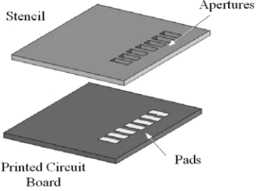
The process of solder paste printing could be accomplished through many methods (i.e. by using a stencil, see Figs. 1 y 2). After this, different types of defects can be detected; some of them are solder paste bridges, too much or too little amount of solder paste, solder out of alignment, and so on. There are some types of defects that can be detected in two dimensions; this is the case of bridges and paste out of alignment. Some other defects require of a three dimensional analysis, like determining the amount of solder paste deposited.
Figure 1. Stencil used in solder paste deposit
In this paper we considered a 2 dimensional analysis for the purpose of detecting defects in solder paste placement. To do so, a referential method was used. As an image reference, we used a printed circuit board without any defects in solder paste deposit. Test images were compared with this reference image in order to detect any difference. If two images were different, then the test image probably had some deposit defect.
3.
IMAGE COMPARISON ALGORITHM91
Journal of Applied Research and Technology
image analysis by means of brightness and contrast characteristics which represent the texture of the analyzed image region only,.
Figure 2. Solder paste deposited on printed circuit board
In order to carry out the analysis, images are divided into non-overlapping N x N pixel rectangular regions. For each test image segment, their bright and contrast histograms are calculated, and these histograms are compared with those obtained from the corresponding reference image segment. To perform histograms comparisons, we used the histogram intersection technique [3, 4]. Taking into account the possible defects in the PCBs [2] and the necessity of reducing the processor’s size, we concluded that images with 256 gray-level are enough to discriminate between different areas, so each pixel is represented by an 8-bit number.
A. Brightness and Contrast Histograms
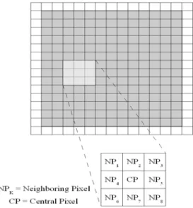
To obtain the histograms, it is necessary to assign a brightness and contrast value to each pixel of the N x N segment. To do so, we take a 3 x 3 pixel window and calculate these values for the central pixel. This is shown in Fig. 3. One thing to consider is that the brightness and contrast values should be calculated just for the pixels in the shady area, since it is not possible to form a window for the peripheral pixels.
A fpga implementation of solder paste deposit on printed circuit boards error detector based in a bright and contrast algorithm, A. De Luca-Pennacchia, et al, 89-102
92
Vol. 5 No. 2 August 2007
Let us call the pixel at the centre of the window “central pixel”, and the 8 pixels surrounding it “neighboring pixels”. In order to obtain the central pixel brightness value, we just calculate the average of the 8 pixels that surrounds it as:
B
CP=
∑
k=18
NP
k8
(1)
Where:
NPk = k-th neighboring pixel value.
BCP = central pixel bright value.
In order to obtain the central pixel contrast value, two averages are needed. First of all, the average value of the neighboring pixels with a value greater than or equal to the central pixel. Then, the average value of the neighboring pixels with a value less than the same central pixel. The difference between these averages is the contrast value.
The following formulas summarize the process for obtaining the contrast:
CP
NP
num
NP
=
gtav
k= kk
≥
∀
∑
sup
81 (2)
CP
NP
numinf
NP
=
ltav
k= kk
>
∀
∑
81 (3)
Where:
gtav = Average of neighboring pixels values greater than or equal to the central pixel.
ltav = Average of neighboring pixels values less than the central pixel.
numsup = Number of neighboring pixels with a value greater than or equal to the central pixel.
numinf = Number of neighboring pixels with a value less than the central pixel.
NPk= k-th neighboring pixel value.
CP= central pixel value.
And from equations 2 and 3, we obtain the contrast value as:
93
Journal of Applied Research and Technology
Where:
CCP = central pixel contrast value.
These brightness and contrast values are calculated for pixels P0, P1 until Pn, where n is the total number
of pixels to be analyzed, which are those appearing in the shady area of figure 3.
B. Histogram comparison
To obtain a likeness measure between image segments, by using the brightness and contrast histograms given, the histograms intersection technique is used [3, 4]. Two image segments will be similar if the following condition is met:
t CH C
BH
B
summin
+
W
summin
>
N
W
∗
∗
(5)
The value of summinBH is obtained by comparing corresponding bins from the reference image bright
histogram and test image bright histogram, and adding minimum values in each bin. The value of summinCH, in the case of contrast histograms, is obtained in a similar way.
The histograms intersection technique says that the sum WB*summinBH + WC*summinCH will approach to
n, the total of pixels analyzed by image, as the test image gets more similar to the reference image. On the one hand, as the image gets more different, the value of the sum WB*summinBH + WC*summinCH will
be smaller. This indicates us that we can define a threshold Nt, in such a way that if the sum is greater
than this threshold, the images are similar. But if it is smaller, the images are different. Saying that two images are similar is equivalent to say that defects in solder paste deposit were not detected. On the other hand, two different images indicate that in test image there is a defect in this deposit.
Values WB and WC are the weights given to the brightness and contrast histograms, respectively. They
appear in formula 5 to diminish brightness change effects among different images. These weights can vary between 0 and 100; however, it is necessary that their sum always equals 100.
Finally, to calculate the likeness measure, integer positive values are used. This last condition allows us to have an easy implementation on FPGA, since it is just necessary to perform integer operations.
A fpga implementation of solder paste deposit on printed circuit boards error detector based in a bright and contrast algorithm, A. De Luca-Pennacchia, et al, 89-102
94
Vol. 5 No. 2 August 2007
Figure 4. Software program window
4. BASIC PROCESSING
In this section, the basic processing unit operation is explained in detail. The design of this unit is important because it let us determine the necessary execution time to analyze an image, as well as the FPGA space required.
A. Image processing system
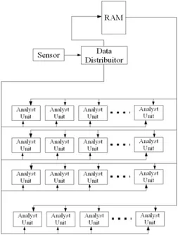
In figure 5, The image processing system architecture is shown. An image sensor generates pixels that are stored in a memory. When the reference image is presented to the system, besides storing pixels in memory, brightness and contrast histograms are calculated for each one of the non-overlapping rectangles that form the image. Later on, when test images are presented, the data distributor takes charge of distributing image segments to each one of the basic process units, with the respective reference image histograms. The process units have the function of generating the brightness and contrast histograms for the received segment in order to compare them with those of the reference image received.
95
Journal of Applied Research and Technology
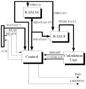
B. Basic process unit.
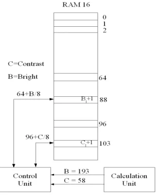
In Figure 6, the basic analyst unit architecture is shown. It consists of two memories. Memory RAM16 has 128 cells, 16 bits each, and it is used to store histograms values. Cells from locations 0 to 63 are used to store the brightness and contrast histograms of the reference image segment. Cells from 64 to 127 are used to store the calculated histograms of the received image segment.
Figure 6. Basic analyst unit
Memory RAM8 has 1600 cells, 8 bits each, and it is used to store pixel values of the received image segment.
The control unit carries out three different functions. Firstly, it is in charge of receiving pixels values from the image segment to be analyzed, as well as reference image histograms. Then, the control unit stores them in their respective memory. Secondly, it selects 3 x 3 pixels windows from the image segment in order to calculate the brightness and contrast values for the central pixel (this is done with the calculation unit), in this way the histograms can be built. Finally, as soon as the histograms are ready, it carries out a comparison process to determine the likeness between them. This last condition is indicated by means of the signal LIKENESS, which is set to 1 if the histograms are similar and 0 otherwise. The signal END is set to 1 to indicate that the result is ready.
1) Windows Selection: For brightness and contrast values calculation, the control unit selects 3 x 3 pixel windows. Window pixels are referred to in the form shown in Figure 7.
A fpga implementation of solder paste deposit on printed circuit boards error detector based in a bright and contrast algorithm, A. De Luca-Pennacchia, et al, 89-102
96
Vol. 5 No. 2 August 2007
The pixel values from the selected window are retained by a 9-register group, and finally these values are presented to the calculation unit. Figure 8 shows the arrangement used.
Figure 8. Register arrangement used to retain window values
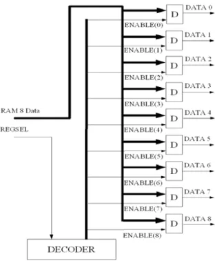
Data coming from the 8-bit RAM are the input of this register group. Signals ENABLE(X) are the outputs from the decoder shown in Figure 8, they enable writing to the register which will receive data from RAM8. To carry out this selection, signal REGSEL, which is generated by the control unit, is used. As soon as the window pixel values are loaded into the registers, the control unit sends a signal to the calculation unit, indicating that the data are ready and it can start calculating the central pixel brightness and contrast values.
97
Journal of Applied Research and Technology
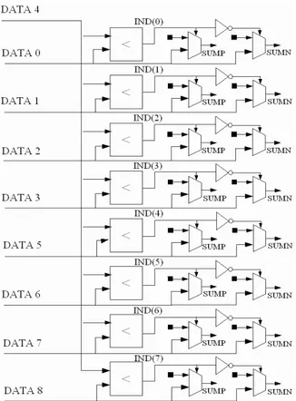
Figure 9. First stage of contrast calculation
In this stage, a group of 8 two-input comparators appears. One of the inputs is the central pixel value (DATA 4). The other input in each comparator is one of the eight neighboring pixels. The comparator outputs are signals IND(X), which are connected to a first group of multiplexers. Whenever any of signals IND(X) is set to 1, the corresponding multiplexer output is equal to the neighboring pixel value to which is connected. If they are set to 0, then the multiplexer output is set to 0.
If a neighboring pixel value is greater than or equal to the central pixel, the respective comparator output (IND(0)) to IND(7)) will be set to 1. This causes the associated multiplexer output to be set to the neighboring pixel value. If the neighboring pixel value is less than the central pixel value, then the comparator output is set to 0; therefore, the multiplexer output is set to 0 too. At the end, neighboring pixel values greater than or equal to the central pixel value appear at the multiplexer outputs from this first group; otherwise, a 0 is assigned to those outputs. These values are inputs to adder SUMP. This adder will generate the sum of these pixels, and this result will be used to obtain the first average necessary to calculate the contrast value.
In order to obtain neighboring pixels values less than the central pixel value, a second group of multiplexers is used. Unlike the first group, each signal IND(X) passes through an inverter. This causes that the behavior of the multiplexers is contrary to that of the first group. As a result, in this second group of multiplexers, the outputs will be set to the neighboring pixel value if this is less than the central pixel value, and to 0 if not. These outputs are the inputs to a second adder (SUMN), which will be used to calculate the other necessary average.
A fpga implementation of solder paste deposit on printed circuit boards error detector based in a bright and contrast algorithm, A. De Luca-Pennacchia, et al, 89-102
98
Vol. 5 No. 2 August 2007
Figure 10. Contrast calculation, second stage
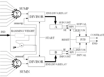
The comparator outputs (IND(X) signals) are the inputs of the module named ``Hamming Weight''. The function of this module is to count the number of 1s presented in the signals IND(X). Since these signals are set to 1 whenever the neighboring pixel value is greater than or equal to the central pixel value, the output of this module gives us the number of these neighboring pixels. This value, together with the output of adder SUMP, is the input of a divider. This is used to calculate the neighboring pixels values average when they are greater than or equal to the central pixel value.
The same module “Hamming Weight'' generates the number of pixels less than the central pixel. This value, together with the output of adder SUMN, is the input to another divider which obtains a new value. One thing to notice is that all the circuits used to calculate contrast before dividers were combinational. Dividers are sequential and they use the same signal clock used in the main circuit. Signal START, coming from the control unit, is used to start the division calculation. This signal is activated just after the window values have been loaded into the registers. Because of this, the FPGA frequency clock should be adjusted to allow that the dividers inputs are ready in a single clock cycle. Signal END from the dividers indicates that the result is ready. Signal AV contains the founded division value, and signal RES contains the residual. If there is a division by zero, this is indicated by setting signal DIV0 to 1.
Module “A” receives the division value found; then, it makes an adjustment if there is a division by zero. In the case of pixels greater than or equal to the central pixel value, a division by zero indicates that all pixels values are less than the central pixel value. In such a case, the average result is the central pixel value. Module “B” carries out a similar function for pixels whose values are less than the central pixel value.
99
Journal of Applied Research and Technology
3) Histograms generation and comparison: The bright and contrast values found by the calculation unit are read by the control unit. In order to form the histograms, the 256 grey-level space is divided into 32 bins. Since the brightness and contrast values have 256 different values, it is just necessary to divide them by 8 so that we can determine the bin they belong to. The brightness histogram begins in location 64 of the RAM16 address space, and occupies 32 locations, one for each histogram bin. Thus, location 64 stores the number of pixels with brightness values from 0 to 7, location 65 stores the number of pixels with brightness values from 8 to 15, and so on. The contrast histogram is carried out in a similar way, but in this case the histogram begins in location 96. Figure 11 shows the histograms generation process.
Figure 11. Brightness and contrast histograms generation
In order to generate the brightness histogram, we need a base value to calculate memory addresses. We take 64 as base value, as this is the starting address of the brightness histogram. The brightness value is divided by 8, and then is added to the base value. This last value indicates the memory location that should be incremented. In the case of the contrast histogram, the base value used to calculate the memory location is 96.
A fpga implementation of solder paste deposit on printed circuit boards error detector based in a bright and contrast algorithm, A. De Luca-Pennacchia, et al, 89-102
100
Vol. 5 No. 2 August 2007
Figure 12. Brightness and contrast histograms comparison
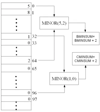
In the case of the brightness histogram comparison, the respective locations are compared (0 and 64, 1 and 65 and so on) and the smaller value is accumulated. This accumulation is done in register BMINSUM, which is shown in figure 12. In the case of the contrast histogram, comparisons are made between locations 32 and 96, 33 and 97, and so on. Register CMINSUM accumulates the smallest values in each location. Finally, formula 5 is used to determine the likeness level of the analyzed image segments.
5. RESULTS
The work done in this project involved the design of the image processing basic circuit represented by the basic analyst unit explained in section 4. With this design, the necessary time to calculate histograms, and its later comparison with its corresponding histogram from reference image, was obtained. This result was used to estimate the necessary execution time to analyze a complete image. Besides, it was possible to estimate the necessary FPGA space to implement the image processing stage.
In our experiments, we used 640 x 480 pixel images. With this image size, it was determined that the value of N, the size of segments that constitute the image, should be 40.
101
Journal of Applied Research and Technology
Using the same synthesis tool, it is possible to estimate the FPGA space needed. At this point, it is necessary to take into account that we want to have an independent inspection system so that all the necessary inspection system functions can be carried out in a single FPGA. We also wanted to have several basic analyst units working in parallel, each working on different image segments. That is why the selected FPGA should have enough space to have several analyst units, besides the necessary area to accommodate other functions.
In order to determine the necessary number of units, first we have to set the maximum time available to process one image. In the case of our example, we proposed an amount of time of 33 milliseconds. Each 640 x 480 pixel image has 12 rows of 40 x 40 pixel segments, this means that each row should be processed in 33/12 = 2.75 ms. So, in the case of the inspection system, we propose to use 2 groups of 16 basic analyzing units (since this is the number of segments per row), each one of them acting on a different line from the image. This way, when the first group finishes receiving data to be processed, the second group can start receiving its own data. Since the 16 units work in parallel, each line can be processed in 0.9 milliseconds working at 50 Mhz. This means that before the second group of units finishes processing the assigned row, the first group has already finished processing its assigned row, and it is ready to receive another one. This is why the selected FPGA should have space to accommodate 32 basic units.
There are FPGAs with the required space, such as the Virtex II and Virtex II pro family. These circuits have additional resources besides programmable blocks. There are circuits with enough memory blocks to program the necessary 32 basic units. That is the case of circuit XC2V4000, where the 32 units would occupy 32 % of the FPGA space, so there is the possibility of having enough space to manage the other functions of the inspection system. There is also the possibility of analyzing the complete image in real time.
6. CONCLUSIONS
An image comparison algorithm based on histograms that represent texture characteristics was elaborated. The design of this algorithm allowed an easy implementation on FPGA with high degree of parallelism and easy scalability.
The basic circuit to implement the algorithm was also designed. This design enabled us to estimate the execution time, and to conclude that real-time image analysis can be achieved, as demanded by modern industry (33 ms in our example).
As a result of the circuit synthesis, there is the possibility of managing the whole inspection system in a single FPGA and, therefore, of having a simple, reliable and more economical system.
7. REFERENCES
[1] TM.J. Swain, D.H. Ballard. Color indexing. International Journal of Computer Vision, 7(1) (1991) 11– 32.
[2] R.P. Prasad. Surface Mount Technology Principles and Practice. Van Nostrand Reinhold, New York, 1989.
[3] E.N. Malamasa, E.G.M. Petrakisa, M. Zervakisa, L.P-D. Legat. A survey on industrial vision systems, applications and tools. Image and Vision Computing, 21(2) (2003) 171–188.
[4] T. Baidyk, E. Kussul, O. Makeyev. Texture recognition with random neural classifier. WSEAS Transactions on Circuits and Systems, 4(4) (2005) 319–324.
A fpga implementation of solder paste deposit on printed circuit boards error detector based in a bright and contrast algorithm, A. De Luca-Pennacchia, et al, 89-102
102
Vol. 5 No. 2 August 2007 Authors Biography
Adriano De Luca-Pennachia
Born in Foggia (Italy), Dr. De Luca graduated in mathematics and physics at Sto. Severo (Foggia), and doctorated in “Nucleonica e Automazione” in Milano (Italy). He has been a member of the SNI since 1986, and has worked for 10 years at the ININ (Mexico), where he has formed various teams of researchers. Dr. De Luca collaborated actively in the group that was awarded the National Prize of Applied Instrumentation in 1974. From 1982 to 1985, he worked for the SGS Thompson in Milano. He obtained the U.S.A. Patent N. 07/483915 in 1991 (“Digital anode to determine the location of electrons in a given surface”), and published a text book, “Digital Systems”, by the Metropolitan Autonomus University in 1992. Dr. De Luca has also authored 92 articles.
Author’s Address: 2508 Instituto Politécnico Nacional Av. San Pedro Zacatenco. México D.F., México. Zip Code. 07360.
Miguel Ángel Sánchez-Martínez
He holds an M. Sc. in electrical engineering and works in the Electrical Engineering Departament at the Research and Advanced Studies Center of the IPN (CINVESTAV).