Brazilian Microwave and Optoelectronics Society-SBMO received 03 Apr 2017; for review 06 Apr 2017; accepted 04 Aug 2017 Brazilian Society of Electromagnetism-SBMag © 2017 SBMO/SBMag ISSN 2179-1074
Abstract—This work presents a new methodology for modeling,
design and implementation of power amplifiers in different technologies. As result of comparison, a flowchart with a new methodology is proposed which can be useful for the designer to design and implement power amplifiers with low, medium and high power devices in different technologies. This paper is divided in 4 parts: The first one is an introduction to the importance of modeling and design techniques in the final implementation of power amplifiers for the modern communication systems. The second one details the modeling process for different technologies, which final result is a unified model. The third part is related with the characterization of high power transistors, with special emphasis on substrate characterization and final implementation of a power amplifier. Finally, in the fourth part, the new methodology is proposed based on the comparisons of previous procedures.
Index Terms—microwaves, modeling, power amplifier, substrate.
I. INTRODUCTION
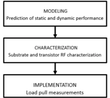
Modern communication systems require RF power amplifiers to operate with large signal in broadband conditions. For 5G systems, requirements will be more demanding; and different technologies such as GaN and LDMOS are currently under investigation. Those two technologies have improved power density compared with traditional compounds semiconductors [1]. It originates problems with power dissipation which creates dispersion and thermal effects [2]. Consequently, for the design of RF power amplifiers using these semiconductors, it is essential to use accurate models that take into account these phenomena. Furthermore, for power amplifier implementation, an accurate substrate characterization is required, in order to get the appropriate input and output impedances for the matching networks. In this paper we will show that through the use of models flexible enough to predict static and dynamic conditions, and a one-port substrate characterization technique, we can demonstrate that it is possible to implement efficiently RF power amplifiers in LDMOS technologies. Based on those steps we propose a new methodology which is summarized in Fig. 1. That methodology will be explained in the following sections.
New methodology for modeling, design and
implementation of RF power amplifiers
Guillermo Rafael-Valdivia, Omar Castellanos Ballesteros.
Brazilian Microwave and Optoelectronics Society-SBMO received 03 Apr 2017; for review 06 Apr 2017; accepted 04 Aug 2017 Brazilian Society of Electromagnetism-SBMag © 2017 SBMO/SBMag ISSN 2179-1074
Fig. 1. Flow chart of the proposed methodology for the power amplifier design.
II. MODELING
Modern communication systems, such us internet of things (IoT) and 5G are currently under investigation; however they will demand the use of different technologies for amplifiers. For instance GaAs is a promising technology for low power and linear applications; and GaN / LDMOS for high power amplifiers for long distance communications. As these 2 technologies behave differently, it makes sense to consider different strategies for modeling. However despite their differences, there are some common characteristics. One of them is the output conductance (gds) and transconductance (gm) frequency dispersion, considered as one of the causes for the memory effects which cause complexity in linearization [3]. In this paper we will call this effect “the frequency dispersion phenomena”. We characterized this effect through I/V pulsed measurements by using the DIVA system provided by Accent Technologies [4]. The measurements were carried out in University College Dublin in the RF and microwave group. As it is shown in Fig. 2, DIVA system is a 2 port equipment, which is able to send and read pulsed voltages in the drain and gate side of a microwave transistor placed in a specific test fixture.
Brazilian Microwave and Optoelectronics Society-SBMO received 03 Apr 2017; for review 06 Apr 2017; accepted 04 Aug 2017 Brazilian Society of Electromagnetism-SBMag © 2017 SBMO/SBMag ISSN 2179-1074
In Fig. 3 it is shown the RF signal sent by DIVA which has a pulse width of 0.2usec with a period about 1ms. This duty cycle allows to measure only the dynamic behavior by keeping the same bias point. The system can measure the static (DC) characteristics of any device and compare them with the dynamic (pulsed) characteristics.
Fig. 3. Voltage waveform at the drain side of a transistor, provided by the DIVA pulsed measurement test system.
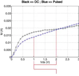
For a NE76038 GaAs low power HEMT, the evidence of the frequency dispersion effect is shown in Fig. 4. We can see difference in the slopes of the IV curves for the static and dynamic conditions. [5]. Furthermore it is possible to set different DC bias points (multibias) and perform pulsed measurements for each case. In this scenario there are also differences between each of the pulsed characteristics. It means that the difference in the slopes are due not only to the bias points positions; but also to the trapping effects as it is indicated in Fig. 5.
Fig. 4. DC and Pulsed IV characteristics for the NE76038 GaAs HEMT device.
Brazilian Microwave and Optoelectronics Society-SBMO received 03 Apr 2017; for review 06 Apr 2017; accepted 04 Aug 2017 Brazilian Society of Electromagnetism-SBMag © 2017 SBMO/SBMag ISSN 2179-1074
Ri G VgiDC Cds Cgd S Cgs VgiRF Ids + -+ -VdiDC VdiRF + -+ -D multipole RC network multipole RC network Vdi (DC+RF) Vgi (DC+RF)
signal equivalent circuit. In fact, this technique uses the pulsed voltages as inputs in the effective voltages equations in order to provide the proper argument for the Ids non-linear equation [4]. The effective voltages equations are shown in (1) and (2), where vdse and vgse are the effective voltages, dvd and dvg are the pulsed voltages, and ki are fitting parameters.
vd
DC
e vd 1 2 Vdi vg 3 4 vg
vds d k k d d k k d . (1)
DC
e vg 5 6 vg Vgi vd 7 8 vd
vgs d k k d d k k d . (2)
The pulsed voltages are extracted from the large signal equivalent circuit by using a four-terminal topology which is shown in Fig. 6.
0 0.5 1 1.5 2 2.5 3 0 0.01 0.02 0.03 0.04 0.05
Vds (V) a)
Id
s
(A)
0 0.5 1 1.5 2 2.5 3 0 0.01 0.02 0.03 0.04 0.05
Vds (V) b)
Id
s
(A)
0 0.5 1 1.5 2 2.5 3 0 0.01 0.02 0.03 0.04 0.05
Vds (V) c)
Id
s
(A)
0 0.5 1 1.5 2 2.5 3 0 0.01 0.02 0.03 0.04 0.05
Vds (V) d)
Id
s
(A)
Fig. 5. Plot of the measured (diamonds) and modeled (squares) pulsed drain to source current obtained for the NE76038 with
the proposed technique. Pulse width 0.2μsec and duty cycle: 0.02%. Extrinsic applied voltages: a) VgsDC=0V, VdsDC=0.5V; b) VgsDC=-1V, VdsDC=0.5V; c) VgsDC=0V, VdsDC=3V; d) VgsDC=-1V, VdsDC=3V. Sweep in gate voltage: 0V to -1V
(uniform step). Similar accuracy was obtained in multibias conditions. [4]
Brazilian Microwave and Optoelectronics Society-SBMO received 03 Apr 2017; for review 06 Apr 2017; accepted 04 Aug 2017 Brazilian Society of Electromagnetism-SBMag © 2017 SBMO/SBMag ISSN 2179-1074
freq (1.000GHz to 10.00GHz)
S
(1
,1
)
S
(3
,3
)
S
(2
,2
)
S
(4
,4
)
For a CGH40010F 10W GaN HEMT transistor, we repeated the same test; but keeping the same bias point and changing only the pulse width. For this case, Angelov nonlinear equation for Ids [2] was implemented. By applying the same effective voltage technique explained for the GaAs transistor, we got a new model in which the dynamic equation was embedded within the Angelov nonlinear equation for Ids. Results are shown in Fig. 7.
Fig. 7.Measured (diamonds) and modeled (squares) pulsed Ids obtained @ VgsDC=-4V, VdsDC=40V for the CGH40010F 10W HEMT transistor. a) Pulse width: 30µsec. b) Pulse width: 5µsec.
One of the properties of this model is that it can be used to model the RF performance. In Fig. 8 it is shown the difference between modeled and measured S-parameters. Furthermore, with the complete characterization of the device, the proposed model can be used to predict the output power vs input power behavior as it is shown in Fig. 9.
Fig. 8. Measured (circles) and modeled (lines) S-parameters for the NE76038 using the proposed method. Extrinsic applied voltages: VdsDC=3V; VgsDC=0V. Similar agreement was obtained in multibias conditions and for other S-parameters.
Fig. 9. Large signal two tone output power performance centered at 2GHz and tone spacing of 4MHz at VdsDC=2V and VgsDC=-0.2V
S1
1
Brazilian Microwave and Optoelectronics Society-SBMO received 03 Apr 2017; for review 06 Apr 2017; accepted 04 Aug 2017 Brazilian Society of Electromagnetism-SBMag © 2017 SBMO/SBMag ISSN 2179-1074
In conclusion for this section, we can say that despite the different non-linear equations for Ids used for the GaAs and GaN devices (COBRA and Angelov respectively), the same methodology for modeling was used and validated. This methodology provided us coherent predictions for the static and dynamic behavior for both technologies.
III. SUBSTRATE CHARACTERIZATION AND POWER AMPLIFIER IMPLEMENTATION
After finishing the modeling process, we focus on the substrate characterization and the power amplifier implementation procedures. Both of them have been carried out in our university. In this section we will demonstrate that it is possible to build power amplifiers according to specific target specs using low cost equipment but well stablished models. Finally we will compare the results with the ones shown in datasheets showing coherence.
A. Substrate characterization
Brazilian Microwave and Optoelectronics Society-SBMO received 03 Apr 2017; for review 06 Apr 2017; accepted 04 Aug 2017 Brazilian Society of Electromagnetism-SBMag © 2017 SBMO/SBMag ISSN 2179-1074
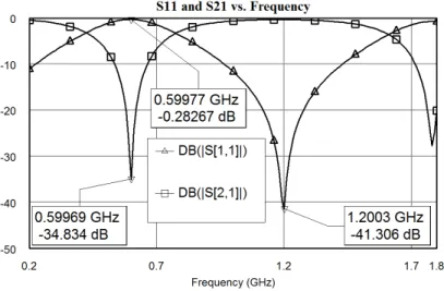
10. We used as test vehicle the low cost FR-4 substrate. The shunt stub is a quarter wave length line at a specific design frequency. It presents a variable impedance to the access ports. So, according to the frequency of the excitation signal, the impedance of the stub can change from open to short. So we will have minimum or maximum values of S11 and S21 at specific resonant frequencies. In our design we decided to set the first resonance frequency at 600MHz (design frequency). We have selected that value considering that its second harmonic must be within the frequency range of our spectrum analyzer (HP8591A). Previous to the measurements, we compared the behavior of the simulated S11 and S21 for our resonator as it is shown in Fig 11.
MLIN L= W= ID= 70.7 mm 3 mm
TL1 MLIN
L= W= ID= 70.1 mm 3 mm TL2 MLEF L= W= ID= 70.1 mm 3 mm TL3 1 2 3 MTEE W3= W2= W1= ID= 3 mm 3 mm 3 mm TL4 PORT Z= P= 50 Ohm 1 PORT Z= P= 50 Ohm 2
Fig. 10.Proposed resonator topology for substrate characterization. Port 2 can be connected to a 30dB attenuator.
Brazilian Microwave and Optoelectronics Society-SBMO received 03 Apr 2017; for review 06 Apr 2017; accepted 04 Aug 2017 Brazilian Society of Electromagnetism-SBMag © 2017 SBMO/SBMag ISSN 2179-1074
Fig. 11. Comparison between the behavior of simulated S11 and S22 for substrate characterization purposes
To perform the measurements, the setup shown in Fig.12 was implemented, where SUT is the substrate under test; Pref represents the reflected power; Pinc the incident power; Pmeas represents the measured power; CF represents the coupling factor; and RL the return loss.
Fig. 12. Block diagram of the proposed method for the 1-port substrate characterization.
Brazilian Microwave and Optoelectronics Society-SBMO received 03 Apr 2017; for review 06 Apr 2017; accepted 04 Aug 2017 Brazilian Society of Electromagnetism-SBMag © 2017 SBMO/SBMag ISSN 2179-1074
(3)
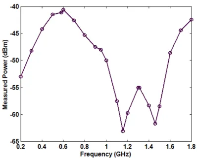
Fig. 13.Measured power (Pmeas or Pmed), using the setup shown in Fig. 12.
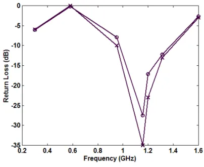
Consequently, those values of Return Loss (RL) can be compared with simulated results, as shown in figure 14. Considering that the geometrical tolerance in the implementation of the circuit (dimension of the lines) is accurate enough, the difference between measurements and simulations is only due to the physical parameters of the substrate: and tan .
Brazilian Microwave and Optoelectronics Society-SBMO received 03 Apr 2017; for review 06 Apr 2017; accepted 04 Aug 2017 Brazilian Society of Electromagnetism-SBMag © 2017 SBMO/SBMag ISSN 2179-1074
Fig. 14. Simulated (x) and measured (o) return loss for the substrate under test.
After the optimization process, we got = 4.4 and tan = 0.02. The average values for these parameters, indicated in [9] are: = 4.7 and tan =0.014. Those values are also coherent with the ones indicated in [10]. In order to confirm the validity of the proposed method, simulations in ADS were performed as well. The results obtained are coherent with the ones that we got through optimization in Microwave Office. The same characterization process was performed with the RF35 substrate; we got = 3.5 and tan = 0.002. The thickness of the substrate was 20 mils (0.5mm). The average values for these parameters, indicated in [11] are: = 3.5 and tan =0.0018. Fig. 15 shows the resonator implemented to characterize the RF-35 substrate.
Brazilian Microwave and Optoelectronics Society-SBMO received 03 Apr 2017; for review 06 Apr 2017; accepted 04 Aug 2017 Brazilian Society of Electromagnetism-SBMag © 2017 SBMO/SBMag ISSN 2179-1074
B. Power Amplifier Implementation
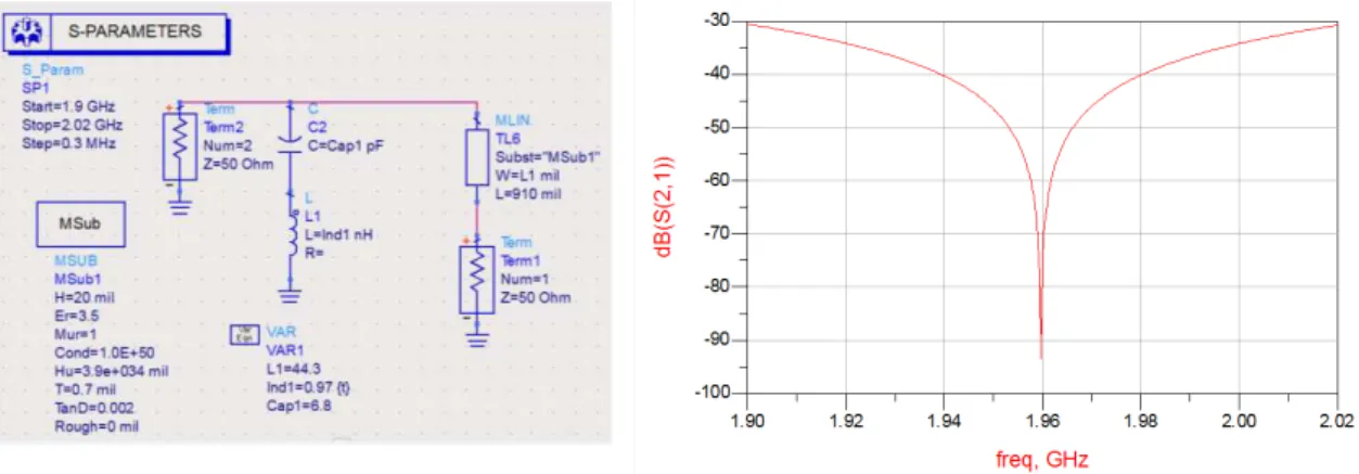
We built a power amplifier using the MRF6S18100 LDMOS device from Freescale Semiconductors (now NXP). We used the RF35 substrate previously characterized with the parameters and dimensions shown in the previous paragraph. According to its datasheet given in [12], this field effect transistor was designed for base station applications, from 1800 to 2000MHz with 100Watts output power and 15dB gain (at P1dB conditions). The recommended bias point for this device is VDD = 28 Volts (typical for LDMOS) at IDQ = 900mA (class AB). In contrast to the conventional bias tee configuration with discrete inductance and capacitors, the bias network in our design uses a quarter wavelength line with a shunt cap in order to provide a virtual RF short circuit at a quarter wave distance from the drain terminal of the transistor. Similar procedure was used to bias the gate side. For both cases we used symmetrical feeders in order to improve bandwidth. Simulations of the bias network design are shown in Fig. 16.
Fig. 16. Bias network simulations for the power amplifier based on the MRF6S18100 LDMOS device.
Brazilian Microwave and Optoelectronics Society-SBMO received 03 Apr 2017; for review 06 Apr 2017; accepted 04 Aug 2017 Brazilian Society of Electromagnetism-SBMag © 2017 SBMO/SBMag ISSN 2179-1074
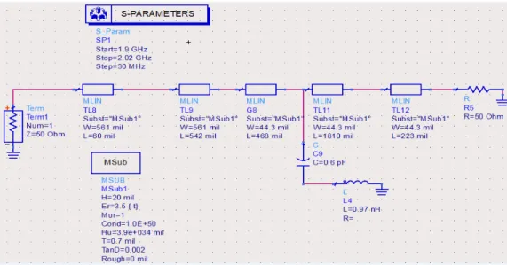
For the design process of the matching networks, instead of using the conventional lumped or discrete matching narrow band techniques optimized only for power or gain; we used wideband techniques with the combination of lumped and discrete components, in order to take advantage of the best properties of each technique. The goal of those networks are to allow the transistor to see the same impedances shown in the load pull data, depicted in Fig.17 in order to meet the target specs (best trade-off between power, efficiency and linearity).
The input and output matching networks are shown in Figs. 18 and 19 respectively, in which the bypass capacitor (modeled as a capacitor in series with a parasitic inductance of 0.9nH) is not shown for visualization purposes of the trajectory of the impedances (Fig. 20 and 21). Its effect is small because it acts like a short circuit at the central frequency. Furthermore, we can see that the impedances obtained in our design (Table I) are similar to the ones provided by the data sheet.
Fig. 18Input matching network for the power amplifier based on the MRF6S18100 LDMOS device.
Brazilian Microwave and Optoelectronics Society-SBMO received 03 Apr 2017; for review 06 Apr 2017; accepted 04 Aug 2017 Brazilian Society of Electromagnetism-SBMag © 2017 SBMO/SBMag ISSN 2179-1074
Fig. 20.Trajectory of the impedances for the input matching network for the power amplifier based on the MRF6S18100 LDMOS device.
Brazilian Microwave and Optoelectronics Society-SBMO received 03 Apr 2017; for review 06 Apr 2017; accepted 04 Aug 2017 Brazilian Society of Electromagnetism-SBMag © 2017 SBMO/SBMag ISSN 2179-1074
TABLE I.SOURCE AND LOAD IMPEDANCES OBTAINED FOR THE FINAL POWER AMPLIFIER DESIGNED WITH THE MRF6S18100 LDMOS DEVICE
Frequency (MHz) Zsource (ohms) Zload (ohms) 1900 2.68-j4.33 1.48-j3.25 1930 2,65-j4,18 1.51-j3.13 1960 2,64-j4,02 1.54-j3.03 1990 2,63-j3,87 1.55-j2.95 2020 2,62-j3,72 1.56-j2.87
To test the performance of our amplifier in different conditions, we performed a power sweep test in three different frequencies in order to extract the gain and capture the output power at P1dB conditions. Our system calculates the gain from every measured power. It stops when the calculated gain compresses 1dB. This allow us to capture the output power at P1dB, whose values are shown in Table II. We selected 3 frequencies: 1930, 1960 and 1990MHz, because this is the frequency band indicated in the data sheet of our transistor [12] (page 1) for its specific application. By doing that, we characterized the amplifier in the edges and in its central frequency. As it is shown in Table II, the obtained values of those parameters agree with the values indicated in the data sheet for the targeted frequency band.
TABLE II.POWER SWEEP MEASUREMENTS FOR THE FINAL POWER AMPLIFIER DESIGNED WITH THE MRF6S18100LDMOS DEVICE
Freq(MHz) G(dB) Pin(dBm) Pout(dBm) Pout(W) IRL(dB)
1930.00 14.56 37.00 50.53 113.06 -18.34
1960.00 14.66 37.01 50.66 116.36 -30.37
1990.00 14.67 36.96 50.63 115.57 -16.41
Brazilian Microwave and Optoelectronics Society-SBMO received 03 Apr 2017; for review 06 Apr 2017; accepted 04 Aug 2017 Brazilian Society of Electromagnetism-SBMag © 2017 SBMO/SBMag ISSN 2179-1074
Fig. 22.Frequency sweep measurements for the MRF6S18100 LDMOS device.
Fig. 23.Final prototype: implemented power amplifier using the MRF6S18100 LDMOS device.
IV. CONCLUSIONS
Brazilian Microwave and Optoelectronics Society-SBMO received 03 Apr 2017; for review 06 Apr 2017; accepted 04 Aug 2017 Brazilian Society of Electromagnetism-SBMag © 2017 SBMO/SBMag ISSN 2179-1074
microwave transistor. After that, by doing S-parameters measurements we can see the RF performance of the model which can be optimized in order to predict the gm/gds dispersion effect.
The second step is the substrate characterization in order to get accurate values for dielectric constant and loss tangent. In this case we demonstrated that we can measure them by using only 1-port measurement and low cost equipment, while traditional methods uses 2 1-port measurements and VNAs. Finally, we designed a LDMOS power amplifier by using loadpull data, in a RF35 substrate previously characterized. By using symmetrical bias networks and lumped/discrete element combinations for the matching networks, we demonstrated that we can reach the appropriate impedances and satisfy the power and gain specs.
ACKNOWLEDGMENT
The authors thank Dr. Apolinar Reynoso- Hernández from CICESE (México) for the measurements on the GaN device. The authors also thank the design team and modeling team of Freescale Semiconductors, Toulouse, France (now NXP) for his valuable support with the LDMOS device.
REFERENCES
[1] δan and al., “High power density InGaP PHEεTs for 26V operation”, 2005 IEEE RFIC Symp. Digest.
[2] GaN HEMT equivalent circuit model with novel approach to dispersion modelling. Justin B. King; Thomas J. Brazil. 2012 7th European Microwave Integrated Circuit Conferenc
[3] Parker1 A. E. Parker, and J.G. Rathmell, “Bias and frequency dependence of FET characteristics,” IEEE Trans.
Microwave Theory and Tech., vol. 51, no.2, pp. 558-592, December 1997
[4] Single function drain current model for MESFET/HEMT devices including pulsed dynamic behavior. Guillermo Rafael-Valdivia; Ronan Brady; Thomas J. Brazil. 2006 IEEE MTT-S International Microwave Symposium Digest [5] IMOC Nonlinear device model for GaN and GaAs microwave transistors including memory effects. G.
Rafael-Valdivia, Anthony Urquizo, Thalia Mendoza. Silvio E. Barbin 2015 SBMO/IEEE MTT-S International Microwave and Optoelectronics Conference (IMOC)
[6] Improved prediction of the intermodulation distortion characteristics of MESFETs and PHEMTs via a robust nonlinear device model. V. I. Cojocaru; T. J. Brazil.1998 IEEE MTT-S International Microwave Symposium Digest
[7] Basque Country University. Physics of Materials Department. "Impedancia. Permitividad eléctrica". Available: http://www.sc.ehu.es/sqwpolim/FISICAII/P2.pdf
[8] JMOE Non-resonant permittivity measurement methods. Sergio L. S. Severo, Álvaro A. A. de Salles; Bruno Nervis, Braian K. Zanini. Journal of Microwaves, Optoelectronics and Electromagnetic Applications, Vol. 16, No. 1, March 2017
[9] "FR4" Available: http://www.farnell.com/datasheets/1644697.pdf
[10]Chen Wang, "Determining Dielectric Constant and Loss tangent in FR-4", UMR EMC. Laboratory technical report: TR00-1-041,. March (2000). Available: http://emclab.mst.edu/documents/TR00-1-041.pdf
[11]RF35. Available: http://www.taconic.co.kr/english/download/RF-35.pdf
[12]Datasheet. Available: http://www.datasheet.hk/view_download.php?id=1127867&file=0068\mrf6s18100n_549062.pdf [13]J.ε. Coupat and al., “True pulse load pull measurement setup for high power transistors characterization”, 2006
ARFTG Conference.