VIDAS
PTDC/EEA-TEL/75217/2006
Deliverable D4.1
VLC Modulation Schemes
Instituto de Telecomunicações
Pólo de Aveiro
Aveiro, July 31st, 2010Deliverable D 4.1:
Modulation Schemes
Authors: Navin Kumar
Mónica Figueiredo
Luis Nero Alves Rui L. Aguiar
Source: Instituto de Telecomunicações - Pólo de Aveiro
No. of pages: 94
Version: 1
Date: March 31st, 2011
This deliverable reports to:
Instituto de Telecomunicações – Pólo de Aveiro i
Contents
Summary ... 1
1.Introduction ... 2
2.Baseband Data Transmission in White Gaussian Noise and Probability of Error ... 4
3.Basic Modulation Techniques ... 7
3.1 On-off Keying – Non Return to Zero (NRZ) ... 7
3.1.1 BER for OOK Modulation ... 9
3.2 Pulse Position Modulation (PPM) ... 10
3.2.1 Bit Error Rate of L-PPM ... 11
3.2.2 Inverted – PPM (I-PPM) ... 12
3.2.2.1 Bit Error Rate of I-LPPM ... 13
4.Direct Sequence Spread Spectrum ... 15
4.1 Introduction ... 15
4.2 DSSS Modulation in VLC System ... 18
4.2.1 Introduction ... 18
4.2.2 Basic Principle ... 18
4.2.3 Sequence Inverse Keying Modulator ... 19
4.2.3.1 Frequency Domain Analysis ... 19
4.2.3.2 The Corresponding Time Domain Analysis ... 22
4.3 SNR and BER of SIK Modulator with AWGN ... 23
4.4 SNR and BER of SIK Modulator in the Presence of External Noise ... 23
4.5 Matlab Simulink Model For DSSS SIK ... 24
4.5.1 Integrate and Dump Decorrelator Receiver ... 25
4.5.2 PN Matched Filter Correlator Receiver... 27
4.5.2.1 PN Code Generator ... 28
5.Uncertainty in Clock Repeaters ... 31
5.1 Clock Repeaters ... 31
5.2 Simulation Framework ... 36
5.3 Performance Analysis ... 41
6.Uncertainty in Cascaded Clock Repeaters ... 45
6.1 Digitally Controlled Delay Lines ... 45
6.2 Performance Analysis ... 47
6.3 Clock Distribution Trees ... 50
Instituto de Telecomunicações – Pólo de Aveiro ii
7.1 Dynamic Jitter in Cascaded Repeaters ... 54
7.2 Bounds for Jitter Accumulation ... 56
7.3 Simulation Results ... 58
8.Performance Results ... 62
9.Concluding Remarks... 68
Modulation Schemes
Project VIDAS: Deliverable D4.1
PTDC/EEA-TEL/75217/2006
Summary
This report presents the analysis of different modulation schemes D4.1 for VLC systems of the VIDAS project.
Considering the final prototype design and application, the deliverable D4.1 was projected. The detail analysis of various modulation schemes are carried out and a robust technique based on direct sequence spread spectrum (DSSS) is followed. DSSS technique though necessitates use of high bandwidth while minimizing the effect of noise. Since the final application does not require very high data rate of transmission but robustness against the noise (external lights) becomes necessary. The analysis is followed by model development using Matlab/Simulink. The performance of both of these systems are compared and evaluated. Some of the simulation results are presented.
Section 1
1. Introduction
Modulation is one of the key processes in communication system. Appropriate and robust modulation techniques allow enhanced performance of the system. The performance of VLC systems is likely to be impaired by the significant high path loss and the shot noise induced by natural and artificial lights. High path loss leads to the use of considerably high optical power levels. In addition, they are also suffered from the speed of optoelectronic devices (LEDs and PIN photodiodes). System performance varies depending on the environment conditions, data rate, technical solutions and implementation of a particular system.
In the application of traffic information broadcast system, the data is received by the receiver installed on moving vehicles. The amount of data received will depend on the data transmission rate, velocity of vehicles and the road length (service area) in which data is receivable. This is given by the relation:
(1) That is, the received data increases with the distance (increase in service area). However, the possibility of interference also increases with distance. Assuming, a vehicle approaching traffic point at a speed of 60kmph will cover 16.6m of distance each second. Considering data rate 100kbps, vehicle speed of 60kmph and a service area between 2.5m to 70m of road length, the amount of received data comes to be approximately 150kbits to 420kbits. Furthermore, a text message in A4 size of paper with 20 font size of Times New Roman Font which can comfortably be read by driver contains approximately 10kbits of data. This means that each second 15 to 42
times of 10kbits of data can be sent by VLC broadcast transmitter and receiver is expected to reliably receive the information. If the transmitted information is repeated a number of times, the driver will have little over 4 seconds to read the message before crossing the service area when green signal remains on (the worst case condition). However, if vehicle needs to stop for green signal there will not be problem in receiving and reading the information.
The above scenario is applicable in normal conditions i.e. when line-of-sight (LoS) channel is free from other disturbances such as fog, rain and dense dust. But under these conditions the channel behavior will vary and thus service area will be affected (as discussed in R3.1). Therefore, a robust modulation technique is needed for this system. DSSS based modulation has been widely used in Radio system and considered robust system especially in noisy environment. However, requirement of transmission bandwidth increases thereby affecting data rate. But, in road safety applications of traffic information broadcast, the data rate is not an important issue. Minimizing the effect of external noise is the most important.
In this report, we focus on one of the most robust modulation technique based on DSSS. The choice for the method is also supported for the low data rate application. The primary measure of system performance for digital data communication system is the probability of error PE [1]. Therefore, we derive a generic expression for PE and SNR for baseband data transmission on AWGN channel.
Section 2
2. Baseband Data Transmission in White Gaussian Noise
and Probability of Error
Consider the binary digital data communication system with transmitted signal consists of a sequence of constant amplitude pulses of either A or –A units in amplitude and T seconds duration. Considering a detector with integrate and dump (Fig. 1a), the performance can be evaluated with probability of error in the received signal. The output of the integrator at the end of a signaling interval is:
(2)
(3) where N is a random variable defined as:
(4)
Since N results from a linear operation on a sample function from a Gaussian process, it is a Gaussian random variable. It has the mean:
since n(t) has zero mean. Its variance is therefore,
(6)
where we have made the substitution E{n(t)n(σ)} = ½ [N0 δ(t – σ)]. Using the shifting property of the delta function, we obtain:
var = ½ (N0T) (7)
Thus the probability density function (pdf) of N is:
(8)
where η is used as the dummy variable for N to avoid confusion with n(t).
If +A is transmitted, an error occurs if AT + N < 0, that is if N < -AT. The probability of this event is:
(9) Which is the area to the left of η = -AT in Fig. 1b. Letting:
, we can write this as:
(10) which is the area to the right of η = AT in the Fig. 1b. The average probability of error is
PE = P(E| +A) P(+A) + P(E| -A) P(-A) . (11)
As P(+A) + P(-A) = 1, we obtain:
(12)
(a) (b)
Fig.1: a) Receiver structure with Integrate-and-dump receiver; b): Illustration of error probabilities for Binary
We can interpret the ratio A2T/N0 in two ways. First, since the energy in each signal pulse is:
(13)
we see that the ratio of signal energy per pulse to noise power spectral density is:
(14)
where Eb is called the energy per bit because each signal pulse (+A or –A) carries one bit of information. Second, we recall that a rectangular pulse of duration T seconds has amplitude spectrum AT sinc Tf and that Rb = 1/T is a rough measure of its bandwidth. Thus,
(15)
can be interpreted as a function of bandwidth (data rate).
Next, we examine the performance of various modulation techniques. We start with most common, based on intensity modulation with direct detection (IM/DD), on-off keying.
Section 3
3. Basic Modulation Techniques
The choice of modulation technique in the design of VLC system remains one of the most important technical issues. Background from IR technology suggests the use of modulation techniques such as OOK, L-pulse position modulation (L-PPM), subcarrier phase shift keying (SC-PSK) and these have been discussed and proposed [2-4]. Utilization of equalization techniques for IR as well as indoor short range VLC has also been proposed by authors in [5, 6]. The use of equalizers substantially increases the receiver complexity while OOK and L-PPM though simple to implement causes interference because of artificial and other sources of light.
In the following sections, we discuss various modulation techniques. We start with OOK, which forms the basic standard for evaluation.
3.1 On-off Keying – Non Return to Zero (NRZ)
On-Off-Keying is the simplest form of amplitude-shift keying (ASK) modulation that represents digital data as the presence or absence of a carrier wave. In its simplest form, the presence of a carrier for a specific duration represents a binary one, while its absence for the same duration represents a binary zero. Some more sophisticated schemes vary these durations to convey additional information. It is analogous to unipolar encoding line code.
The block diagram of a typical receiver system employing IM/DD is shown in Fig. 2. Information bits are the inputs to the modulator (NRZ or Manchester) at a bit rate of Rb (bit per second (bps)). Pulse waveforms produced by the modulator for each bit drive the optical
transmitter. The intensity-modulated optical signal passes through a time-dispersive multipath channel that is fully characterized by its impulse response hc(t). However, multipath channel can be ignored in this application. The incoming optical signal is converted to an electrical signal by the photodiode by using direct detection. This electrical signal is comprised of a distorted replica of the transmitted signal and shot noise, nsh (t), as well as fluorescent light periodic interference,
nfl(t). The high pass filter (HPF) at the receiver front end, after the photodiode, is modeled as a first-order RC filter with a cut-off frequency of fo. Matched filtering using Integrate and dump filter is assumed for both modulation schemes. The impulse response of the matched filter for both modulation schemes is also depicted in Fig. 2. In the absence of fluorescent light and inter symbol interference (ISI), this corresponds to the optimum maximum-likelihood (ML) receiver [7].
The peak amplitude of the received signal pulses is A and is directly proportional to the optical power, i.e., A= 2R Popt, where R is the photodetector responsivity and Popt is the average received optical power [2, 8]. The power spectral density (PSD) of the Gaussian shot noise nsh (t) is denoted by N0. The shot noise PSD is dependent on the total DC-generated photocurrent, i.e.,
N0 2e(IB + ib), where IB is the DC photocurrent generated by stationary ambient lighting and ib is the DC level of the fluorescent light interference. For both modulation schemes the transmitted signal waveform can be described as an infinite series of time delayed replicas of the basic pulse waveform p(t):
(16)
where p(t) is the rectangular pulse of duration Tb = 1/Rb. However, if signal is Manchester, the
p(t) is the alternating pulse of the same duration with mid-bit transition.
Ignoring noise components, the received signal pulse r(t) at the input of the matched filter will be:
(17)
where hF (t) is the impulse response of the HPF and * denotes convolution.
3.1.1 BER for OOK Modulation
On-Off-Keying transmitter emits a rectangular pulse of duration 1/Rb and of intensity 2P to signify a one bit, and no pulse to signify a zero bit. The bandwidth required by OOK is roughly Rb . The BER is given in terms of minimum distance between two bits. In this type of receiver design, the receiver will choose that signals from the set of known signals that is closest to the received signal. Since the receiver observes which of the possible signals is closest to the received signal, it stands to reason that it is less likely to make an error due to noise or other errors when the other signals are further away.
For the case of OOK the BER is given as:
(18)
Also, in terms of error function1, it is given as:
(19)
Power required by OOK to achieve a given BER is:
(20)
For any other modulation scheme to achieve the same error probability, the required power is approximately: (21) 1 and also,
3.2 Pulse Position Modulation (PPM)
Higher average power efficiency can be achieved by employing pulse modulation schemes in which a range of time dependent features of a pulse carrier may be used to convey information.
PPM has been used widely in optical communication systems. It is a scheme where the pulses of equal amplitude are generated at a rate controlled by the modulating signal's amplitude. During PPM transmission, signal pulses are fixed width and amplitude, but the actual number is represented by pulse position in time.
L-PPM utilizes symbols consisting of L time slots (chip). A constant power L.P is transmitted during these chips and zero during remaining (L-1) chips. Hence, encoding log2L bits in the position of the high chip. If the amplitude of transmitted waveform is A, average transmitted power of 2PPM is A/2, that of 4PPM is A/4, and for L-PPM is A/L. For any L greater than 2, PPM requires less optical power than OOK. In principle, the optical power requirement can be made arbitrarily small by making L suitably large, at the expense of increased bandwidth.
For a given bit rate, L-PPM requires more bandwidth than OOK by a factor of L/log2L i.e. 16-PPM requires four times more bandwidth (BW) than OOK. The bandwidth required by PPM to achieve a bit rate of Rb is approximately the inverse of one chip duration, B = L/T [9]. In addition to the increased bandwidth requirement, PPM needs (compared to OOK) more transmitted peak power and both slot and symbol-level synchronization [10].
In the absence of multipath distortion, L-PPM yields an average–power requirement that decreases steadily with increasing L; the increased noise associated with a (L/log2L)-fold wider receiver noise BW is out weighted by the L-fold increase in peak power.
Fig. 3 shows the block diagram of the L-PPM system. Input bits, at rate Rb, enter a PPM encoder, producing L-PPM symbols at rate Rb/Log2L. Each symbol contains a single sample of unit amplitude and (L-1) samples of zero amplitude. The PPM symbols are converted to a serial sequence of chips at rate LRb/log2L and passed to a transmitter filter whose impulse response p(t) is a unit-amplitude rectangular pulse of duration log2L/LRb. The chips are scaled by the peak detected photocurrent LRP and shot noise n(t) and fluorescent-light interference nfl(t) are added. The receiver employs a unit- energy filter r(t) matched to p(t) which is followed by high pass filter h(t). The filtered signal is sampled at rate LRb/log2L and passed to a comparator that determines which sample in each L-length block has the largest value thus yielding the output bit sequence. Without fluorescent light and high pass filtering the receiver is ML receiver.
In this type, each signal is orthogonal of the form:
Xm = [0, 0, ……, bh, 0, 0] (22)
where the non-zero term is in the m-th position. Thus, every signal is the same distance from every other signal. Fig. 4 illustrates the waveforms from pulse modulators.
3.2.1 Bit Error Rate of L-PPM
For L orthogonal signals, there are (L-1) other signals at the minimum distance, and the error probability is independent of which signal is transmitted. Symbol error rate can be derived from minimum Euclidian distance (dmin):
(23)
where dmin for L-PPM is given as:
(24)
Hence, the symbol error rate for L-PPM is given as:
Fig. 3: Block diagram of L-PPM System
Fig.4: Illustration of L-PPM and I-LPPM waveforms
t A Tb/4 0 1 00 11 Tb 2Tb 0 OOK=>2PPM 4PPM I-4PPM t A 001 010 Tb/8 2Tb Tb 0 1 0 8PPM I-8PPM OOK=>2PPM Tb/4 Tb/8 symbol symbol Tb/2 3Tb/4 3Tb/8 4Tb/8
(25)
(26)
BER - We assume that symbol ‘1’ (corresponding to chip sequence bk of a single one followed by (L-1) zeros) was transmitted and we assume k = L. Therefore, probability of bit error can be approximated as:
(27) So that, (28)
The average optical signal power required to achieve a given SER for an L-PPM system can be found by solving for Pav:
(29)
(30)
That is, L = 2 yields a sensitivity for 2-PPM that is identical to OOK. We see that, for any L greater than two, the optical power required by L-PPM is smaller than that required by OOK.
It can also be noted that, 2-PPM has the same power efficiency as OOK but requires twice the bandwidth. It is apparent that 4-PPM is particularly attractive because it has the same bandwidth requirement as 2-PPM but requires 3.8dB less optical power. As L increases from 4 to 16, the bandwidth requirement increases from 2Rb to 4Rb, while the sensitivity increases from 3dB better than OOK to 7.5dB better than OOK.
For a given transmitter power, background illumination power, and bit rate, it is desirable to maximize the allowable distance between transmitter and receiver, which is equivalent to maximizing the power efficiency.
3.2.2 Inverted – PPM (I-PPM)
In the case of conventional PPM, we set only one pulse among L sub intervals. Average transmitted power, i.e. LED brightness, falls to 1/L when the peak amplitude is not changed. Of course, LED brightness can be made to equal with other modulation methods if we increase the
amplitude L times (practical limitation with power constraint). I-PPM yields higher brightness than conventional PPM. Inverting the pulse position of conventional PPM, we obtain I-PPM (as shown in Fig. 4. The optical intensity is ‘off’ during the 1-th sub-interval and ‘on’ everywhere else. For example, in case of 4-PPM light is on equivalent to 3-chip duration, making the LED three times as bright as conventional 4PPM. When amplitude of the transmitted waveform is A, average transmitted power of I-4PPM is 3A/4. That is, the average transmitted power of I-L-PPM is (L-1)A/L.
This modulation technique is particularly suitable in the indoor environment for the reason that illumination is better.
3.2.2.1 Bit Error Rate of I-LPPM
In the case of inverted multilevel PPM, the symbol error rate for the inverted L-PPM is given as:
(31)
(32)
and the BER is therefore;
(33) The average optical signal power required to achieve a given SER for an I-LPPM system can be found by solving for Pav:
(34)
(35)
From the simulation results it is observed that L-PPM forms of modulation techniques are power efficient and can increase the data transmission rate. However, that may result in inter-symbol interference and increased bandwidth. On the other hand, I-LPPM is suitable for indoor scenario where power is not a constraint that is required illumination remains to be in place. This means, they are not power efficient. However, the effect of noise on the systems remains an issue and in VLC systems the noise effect needs to be minimized. This implies that a different approach must be considered. From the background on RF technology we know the bandwidth
spreading can minimize the effect of noise on the channel. In the next section, this issue is discussed in detail using DSSS technique.
Section 4
4. Direct Sequence Spread Spectrum
4.1 Introduction
In a direct sequence spread spectrum communication system [11], the spectrum spreading is accomplished before transmission through the use of a spreading code that is independent of the data sequence. The same spreading code is used in the receiver (operating in synchronism with the transmitter) to de-spread the received signal so that the original data may be recovered. The information-bearing signal is multiplied by a spreading code so that each information bit is divided into a number of small time increments. These small time increments are commonly referred to as chips. In this process the narrow bandwidth of the information-bearing signal is spread over a wide bandwidth with a factor L which equals the length of the spreading sequence.
Spread-spectrum communication techniques may be very useful in solving different communication problems. The amount of performance improvement that is achieved through the use of spread-spectrum, relative to an unspread system, is described in terms of a so-called processing gain (PG) factor. In spread-spectrum modulation an information-bearing signal is transformed into a transmission signal with a much larger bandwidth. The transformation is achieved by encoding (spreading) the information bearing signal with a spreading code signal. This process spreads the power of the original data signal over a much broader bandwidth, resulting in a lower power spectral density than the unspread information signal. When the spectral density of the resultant spread spectrum signal starts to merge with or fall below the background noise level, the DSSS communication signal enters a state of low visibility or
perception, making it hard to locate or intercept. This communication mode is commonly referred to as low probability of interception (LPI), and offers a form of security, which has previously been exploited for military applications, but are presently increasingly applied to a host of commercial applications. The PG of the spread-spectrum system can be defined as the ratio of transmission bandwidth to information bandwidth:
(36)
where BT is the transmission bandwidth, BB is the bandwidth of information-bearing signal, Tb is the one bit period of the data signal, Tc is the one chip period of the spreading code, Rc is the chip rate of the spreading sequence, Rb is the bit rate of the data signal and L is the length of the spreading code.
The receiver correlates the received signal with a synchronously generated replica of the spreading code signal to recover the original information-bearing signal. This implies that the receiver must know the spreading sequence or code used to spread or modulate the data.
The basic spreading process in a direct sequence spread-spectrum system is illustrated in the conceptual block diagram of a DSSS transmitter and receiver in Fig. 18a and Fig. 18b. The information-bearing signal d(t) is multiplied by the spreading code c(t) and modulated onto a RF carrier frequency to obtain a final spread output signal s(t);
(37) where fRF is the carrier frequency.
The incoming signal is received by the RF front-end consisting of basically a noise reject band pass filter, a low noise amplifier (LNA) and a mixer to down-convert the RF signal to intermediate frequency (IF). This DSSS IF signal is de-spread and band pass filtered, where after the de-spread signal is demodulated by means of a binary phase shift keying (BPSK)
Fig. 5(a): Conceptual Block Diagram of DSSS Fig. 5(b): Conceptual Block Diagram of DSSS Transmitter
demodulator to recover the original information-bearing signal d(t). The process of spreading and dispreading signal in frequency domain is shown in Fig. 6.
A DSSS system employing complex spreading sequences may include several advantages, such as offering perfectly constant envelope output signal including the possibility to generate a single side band (SSB) DSSS signal with theoretically up to 6dB more PG than offered by conventional double side band (DSB) system while exhibiting comparable auto and improved cross correlation properties compared to any other binary (DSSS) presently employed [11].
Fig.6: Signal in frequency domain demonstrating the spreading-
4.2 DSSS Modulation in VLC System
4.2.1 Introduction
Spread spectrum modulation technique can minimize the affect of interference according to the processing gain advantage. While the additional bandwidth requirement of a spread-spectrum modulation scheme reduces the system bandwidth efficiency, the processing gain of the spread spectrum technique helps to combat artificial light interference effects and multipath dispersion (if any) without the need for extra circuitry such as equalizers. A form of DSSS technique called sequence inverse-keying (SIK) [12] is able to combat these two important channel impairments and is a potential modulation format for the low rate VLC in the outdoor.
4.2.2 Basic Principle
The use of DSSS to an OW system is based on the basic principle of unipolar-bipolar correlation [13]. In radio systems, DSSS uses bipolar spreading sequences that cannot be used as such in the all-positive (unipolar) optical medium. The technique called unipolar-bipolar sequencing that allows the same spreading codes of radio systems to be used in optical systems are employed instead. Unipolar-bipolar sequencing, which involves transmission of a unipolar spreading sequence and correlation with a bipolar version of the same spreading sequence, preserves the correlation properties of bipolar-bipolar sequencing although with the introduction of a fixed dc offset.
At the transmitter, a unipolar spreading sequence is modulated by binary data such that the sequence is transmitted for a binary ‘1’ while the inverse (complement) sequence is transmitted for a binary ‘0’. This type of modulation is called as SIK. The resulting spread spectrum signal, which uses a rectangular NRZ chip waveform, intensity modulates the visible light source (LEDs), by on-off keying. At the receiver, the optical signal is detected and processed. The spread signal may be AC coupled prior to de-spreading in order to remove the unwanted DC signal components introduced by the optical channel. AC coupling does not alter the correlation properties of the spreading sequence, thus de-spreading can use the bipolar version of the unipolar spreading sequence. For single correlator detection, the de-spread signal is integrated over the data bit period Tb and sampled at intervals of t = Tb. The sample value at the correlator output is zero-threshold detected such that either a positive or a negative sample results a binary ‘1’ or ‘0’ estimate of the transmitted data bit, respectively.
4.2.3 Sequence Inverse Keying Modulator
Fig. 7 shows the schematic diagram of the transmitter and receiver of SIK system. The modulator part basically performs digital operation of X-NOR where incoming data bit is modulated by a pseudo noise random data of many times higher bit rate than the data bit. Thus, the transmitted data is said to be spread. A similar operation is needed at the receiver to de-spread the incoming sequence from channel. For better understanding, frequency domain analysis is presented followed by equivalent time domain analysis.
4.2.3.1 Frequency Domain Analysis
A frequency domain analysis of the operation of DSSS SIK is presented to give a better understanding. Let us consider:
Information data: B(t)
Unipolar spreading signal: s(t) Chip period: Tc
Impulse response of the channel: h(t) Interference due to light sources: f(t)
The pseudo noise (PN) generator s(t) may be written as:
(38)
where a(i) is the unipolar PN sequence, p(t) is the pulse shape, N is the code length, so that each bit has N chips (N * Tc = Tb) with Tb is the period of data bit. B(t) is combined with spreading sequence s(t) to spread the transmitted signal which is given as:
(39)
where ρ is the energy of a pulse and ´ ´ is the SIK operator i.e. PN sequence is transmitted for data ‘1’ and inverse of PN sequence for data ‘0’. The PSD of x(t) is given as:
(40)
where S(f) is the Fourier Transform (FT) of s(t) and Фb(f) is the PSD of the information data bits
B(t). Before de-spreading, the received signal r(t) is:
(41)
The PSD of the signal r(t) is given as:
(42)
where,
H(f) = the F.T of the channel impulse response, h(t) Фn(f) = the PSD of the Gaussian Noise,
Фf(f) = the PSD of interference caused by light sources.
We consider first, the light source as artificial consisting of mainly incandescent and fluorescent lamps. Therefore, the PSD of the output signal y(t) after de-spreading and without filter as in Fig. 8a is given as:
(43)
And the desired signal power is therefore,
(44)
The Gaussian distributed noise power is given as:
(45)
where,
(46)
with q is the electronic charge, R being the responsivity of the photo diode receiver, Pinf is the interference power (optical background) and Bn is the bandwidth.
(47) The light interference power can be calculated (for example, using Moreira’s model) as:
(48)
where Pf is the average optical power of interference signal and N is the spreading gain. Therefore, the signal to interference ratio is given as:
(49)
The operation of DSSS modulation and demodulation and the spectral results are shown in Fig. 9. However, when a filter is added (as shown in Fig. 8b) to the output before passing it through decision making device (integrator, not shown), the PSD can be given as:
(50) where the H’(f) is the response of the filter.
A low pass digital filter is included so that only signal of interest is allowed. This is expected to enhance the performance of DSSS receiver.
4.2.3.2 The Corresponding Time Domain Analysis
The unipolar binary data b(t) from traffic information source given as:
(51)
for bk Є {0,1: - ≤ k ≤ }. bk is XNORed with unipolar spreading sequence s(t):
(52)
where, sn Є {0,1: n = 0,1, …..N-1}, where N is the sequence length, Tc is the chip duration and
Tb = NTc. The duration of N chips in one period of the spreading sequence is equal to the bit duration. In fact, the XNOR function realizes the SIK modulation format. The spread data is then convolved with the transmit pulse wave [xt(t)] and the resulting signal is used to intensity modulate the LED light source. The optical signal is characterized by an average optical power P and a peak pulse power 2P. The light propagates through free space channel, get added with noise and then detected by photodiode. The photodiode responsivity is given by (R=A/W). The detected photocurrent for the LoS case can be given as:
(53)
where, Pav; is the mean optical power of the LOS signal impinging the photocurrent,f(t); is the interfering signal at the output of the photodiode due to ambient light n(t); is the channel noise process (including amplifier thermal noise and shot noise) and considering additive white Gaussian noise with power spectral density N0. The operator is the SIK function given as:
(54) where, b'(t) and s'(t) are the bipolar version of b(t) and s(t).
The f(t) as discussed in [14] has the DC component R.Pf and AC component R.Pf f'(t) with Pf as the average interfering power from other sources of light. Substituting these values in received signal results in:
(55) This received signal is AC coupled and so the DC term will be removed. The signal is then given as:
(56) This signal is now multiplied by s(t) and then integrated over one data bit duration and threshold detected which is set to zero. Therefore, the correlator output becomes:
(57)
(58) where, b Є {1, -1} denotes the present data bit which is desired signal term. The second term is the interference by light while the third term is the noise.
4.3 SNR and BER of SIK Modulator with AWGN
Considering only AWGN channel, the BER from (58) can be written as:
(59)
That is, the performance of SIK in an AWGN channel has the same theoretical performance as OOK.
4.4 SNR and BER of SIK Modulator in the Presence of External Noise
The mean (µz) and the variance σz2 of z(Tb), at the correlator output from equation (58) can be given as:
(60)
where σm is the standard deviation of f'(t) and the same as the RMS value. The value given in [15] is around 0.3593. The SNR at the output of correlator is given as:
(62) Or (63)
where P is the optical power. If √(N0Rb) = R.Pn denote a noise equivalent optical power. The second term in the denominator can also be written as 1/SNRopt which is the optical signal-to-noise power ratio. Thus equation (62) can be written as:
(64)
We also define signal-to-interference ratio (SINR) as:
(65)
Substituting this in above equation results in:
(66)
when we assume data bit ‘+1’ and ‘-1’ to be equiprobable, the BER will be:
BER = Q[√(SNR)] (67)
The performance parameters in terms of BER and SNR, data rate and power requirements are analyzed and simulated. The simulation results show that DSSS SIK modulation is an effective method for countering the effect of noise, especially interference noise from the artificial light sources. They also show that increase in PG improves the system’s performance. However, more PG implies a lengthy pseudo noise (PN) sequence which limits the data rate. Therefore, a compromise value of PG between 10-31 can be used.
The following sections present description of system models using Matlab/Simulink and their validity through simulation.
4.5 Matlab Simulink Model For DSSS SIK
As simulation exercise, Matlab models are developed in Simulink. We have developed two decorrelator receiver architectures for dispreading spread spectrum signals: integrate and dump filter, also called as active correlator and PN matched filter. They are optimum from a
SNR point of view. The motivations behind the study are: (i) to compare the performance of DSSS SIK using both of these receiver architectures, and (ii) implement the architecture that is most suitable in FPGA. In addition, we have also introduced a delay network in the channel to simulate simultaneous reception of a strong reflected or non-direct ray. The gain of this secondary ray is set to one fourth of the direct ray. In the study, it is observed that as the gain of the secondary ray increases, the BER performance decreases. Behavior of both the architectures because of secondary non-LoS ray is found to be the same.
4.5.1 Integrate and Dump Decorrelator Receiver
This receiver operates correctly only when the local PN sequence is accurately matched and correctly timed, with respect to the spreading code within the received signal. Synchronization becomes difficult too and it is very slow process. Fig.10 shows the basic structure of integrate and dump filter decorrelator. The Simulink model structure is shown in Fig.11. The receiver block connected by dashed lines are the integrate and dump decorrelator while the receiver block connected by solid lines shows the discrete FIR based PN matched decorrelator. Different functionalities were achieved using different blocks. Here we have considered both the conditions; DSSS SIK with AWGN channel only and with additional noise in the model. The model consists of Bernouli binary generator as data source, PN sequence generator as spreading code, SIK subsystem to obtain the SIK function, data format converters, AWGN channel, uniform noise generator, Integrate and Dump filter, threshold detector and error detection block.
The integrate and dump block creates a cumulative sum of the discrete-time input signal, while resetting the sum to zero according to a fixed schedule. When simulation begins, the block discards the number of samples specified in the Offset parameter. After this initial period, the
∫
dt 0 NcTc г PN Sequence NcTc 2NcTc t Rc Rc Out to Thresold Detector Channel Outblock sums the input signal along columns and resets the sum to zero every N input samples, where N is the Integration period (one data bit) parameter value. The reset occurs after the block produces its output at that time step. This blocks also results in a delay of one bit. The parameters setting are shown in Table 1.
TABLE 1: Simulink Model Simulation Parameter Settings
Block Parameter(s) and Value
Bernouli Binary Random Generator Probability of a 0 and 1 = 0.5,
Sample Time = 1
Pseudo Noise Generator
Generator Polynomial: [1 0 0 1 1], Sample Time : 1/10,
Output mask vector : 0
Additive White Gaussian Noise
Signal-to-Noise Ratio (Eb/No ) : 1-16dB, Number of bits per symbol: 1,
Input signal power, referenced to 1 ohm (watts): 1, Symbol Period: 1/10
Uniform Noise Generator
Noise Lower Bound: -0.25, -0.35, 0, Noise Upper Bound: +0.25, 0.35, 0.50, Sample Time: 1/10
Signum Output 1 for positive input, -1 for negative input, and 0 for 0
input, y = signum(u)
Integrate and Dump Filter
Integration period (number of samples): 10, Offset (number of samples): 0
Output intermediate value
Error Rate Calculation Receive delay: 1,
Computation delay: 1
Simulation Time Free running Up Counter
107Seconds Counting from 0 – 9 Output : count and hit Samples per output frame : 1
Discrete FIR Filter
Delay Network
Embeded MATLAB function
Direct form structure Numerator coefficients :
[ 1 -1 -1 1 -1 -1 -1 1 1 1 ] Initial state: 0
Sample time : 0.1 Delay unit: Sample Delay: 1 sample Initial condition: 0 Gain: 0.25 Sample time: 0.1
4.5.2 PN Matched Filter Correlator Receiver
A typical PN matched filter decorrelator is shown in Fig.12. This filter implements convolution using an FIR. The FIR coefficients are chosen to be time reverse of the PN sequence. For example, the PN sequence (pni) and filter coefficients (Fci) can be given as:
pni = [pn0 pn1 pn2 pn3 pn4 pn5 pn6] = [-1 +1 +1 +1 -1 -1 +1],
Fci = [Fc0 Fc1 Fc2 Fc3 Fc4 Fc5 Fc6] = [+1 -1 -1 +1 +1 +1 -1].
The output of the FIR is the convolution of the received (incoming) signal bc with the FIR coefficients Fci. Because of time reversion, the output of the filter is the correlation of rc
Fig.11: MATLAB Simulink Model for PN matched decorrelator and Integrate & Dump decorrelator
Fig.12: PN Matched Filter Decorrelator using FIR
Bernouli Binary Data Source
PN Sequence Generator
SIK AWGN &
Other Uniform Channel Noise PN Matched Decorrelator FIR Receiver Error Detector 0.000124 124 1000000
Integrate & Dump Decorrelator Receiver SIK ⌠dt 0 Tb Delay Non-Loss Path Tc Tc Tc bc(t) bc(t-Tc) bc(t-2Tc) bc(t-3Tc) bc(t-(Nc-1)Tc) NcTc 2NcTc Fc0 Fc1 FcNc-2 FcNc-1 Rc[bc,Fc] Fc - FIR coefficient bc - incoming bits rc - received bit Rc[rc,Fc] Delay Line
with the PN sequence, given by:
= (68)
In Fig.12, the large peak confirms that the correct code is indeed being received and provides accurate timing information for the synchronization of the received signal. The peak output of FIR PN matched filter is the decorrelated data and the polarity of the large correlation peaks indicates the data value.
Though, both the receiver architectures have been discussed here but choice for FIR implementation in FPGA is for the reasons that the code length is small and synchronization time is faster. The Table 2 above provides important comparison between two architectures.
4.5.2.1 PN Code Generator
The PN code characterizes by its process gain and the overall complexity. A novel PN code has been designed to be used in this model. It is comparable and close in the performance to the popular Barker code used in DSSS radio system. A PN sequence length of 10 is developed as a compromise between spectrum spreading and processing gain. It offers almost the same autocorrelation properties as of Barker code. In addition, it is easier to implement. In this code, we have a sequence length of 10 given as:
PN code = +1 +1 +1 -1 -1 -1 +1 -1 -1 +1.
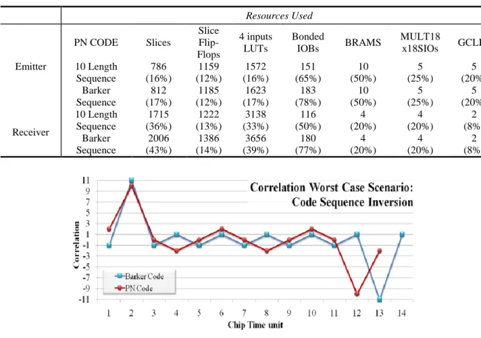
Both exhibit very good correlation properties avoiding false acquisitions and degradation at DSSS receiver. Table 3-A and Table 3-B illustrate a comparison between both codes. While Table 3-A provides general characteristics, Table 3-B gives the differences in implementation in resources used by two codes. Fig.13 shows the worst correlation case scenario, which occurs when the sequence finds its complement. In this case both codes exhibit small partial correlation peaks.
TABLE 2: Comparison of Two Architectures
Sync Process Hardware Resources Suitability Operational Requirements
Integrate and Dump
Slower
(2Nc2Tc) Simple
Long
sequence Needs accurate timing
FIR Decorrelator Faster
(NcTc) Number of Filters equal Nc
Smaller Sequence
length
No need
The code is DC-balanced, i.e. it has the same number of positive and negative logical levels during all communication which reduces the DC component significantly. Furthermore, the number of identical consecutive bits is not more than 3 which avoids voltage drop in analog circuitry. These two characteristics are very important in VLC, where the information is carried by intensity modulation and demodulated by direct detection (IM/DD). Also, it is easier to obtain a relation between chip rate and data rate, when the code has an even length number.
TABLE 3-A: Comparison of Two Codes
Code Sequence Correlation
Peak Side Lobe Observations
New PN Code
+1+1+1-1-1-1+1-1-1+1
(10) ±10 ±2
DC balanced Low resource usage Easy implementation Processing Gain: 10.0 dB Barker Code +1+1+1−1−1 −1+1−1−1+1−1 (11) ±11 ±1 Almost DC balanced Higher resource usage
More Complex Processing Gain: 10.4 dB
Table 3-B: Comparison of Resources Consumed by Code Implementation
Resources Used Emitter PN CODE Slices Slice Flip-Flops 4 inputs LUTs Bonded IOBs BRAMS MULT18 x18SIOs GCLKs 10 Length Sequence 786 (16%) 1159 (12%) 1572 (16%) 151 (65%) 10 (50%) 5 (25%) 5 (20%) Barker Sequence 812 (17%) 1185 (12%) 1623 (17%) 183 (78%) 10 (50%) 5 (25%) 5 (20%) Receiver 10 Length Sequence 1715 (36%) 1222 (13%) 3138 (33%) 116 (50%) 4 (20%) 4 (20%) 2 (8%) Barker Sequence 2006 (43%) 1386 (14%) 3656 (39%) 180 (77%) 4 (20%) 4 (20%) 2 (8%)
Furthermore, this novel PN code is easily implemented using a linear feedback shift register (LFSR) with four (n = 4) registers and a counter. The LFSR generates a maximum length sequence (m-sequence) code of (2n -1) 15 bits. This sequence is truncated to 10 using a counter, resetting the LFSR every 10 times. In order to ensure the correct sequence bits, the initial value of the LFSR four registers must be equal to the four initial bits of the PN sequence.
The Simulink model structure is shown in Fig.11 with blocks connected by solid lines. The delay network which simulates the behaviour of non-LoS signal is also shown in the figure. The parameters selected are described in Table 1.
Section 5
5. Uncertainty in Clock Repeaters
Clock repeaters are used in digital synchronous systems with two main purposes - to amplify the clock signal or to introduce intentional delay. According to the desired performance, the designer can choose from a large variety of different physical implementations. Traditional performance metrics include the repeater’s delay, power consumption and implementation area. Delay uncertainty is known to be roughly proportional to the cell’s propagation delay, but there is still no practical means to accurately quantify this relationship.
5.1 Clock Repeaters
Propagation delay through conventional clock repeaters depends on their size and spacing and cannot be manipulated once the chip is manufactured. These repeaters are here called Static Delay Repeaters (SDRs). In the last decade, Post-Silicon Tunable (PST) clock repeaters have gain popularity, as their propagation delay can be statically or dynamically manipulated to compensate for Process Voltage and Temperature (PVT) variations [16]. In opposition to SDRs, they are hereafter referred as Tunable Delay Repeaters (TDRs). Besides being used as amplification stages in clock distribution networks, both SDRs and TDRs are the basic building blocks of other clocking systems, as Delay Locked Loops (DLLs) [17], Phase-Locked Loops (PLLs) [18], Digitally Controlled Oscillators (DCOs) [18, 19], Dynamic Random Access Memory (DRAM) interface units [20], Deskewing (DSK) circuits [21] or spread-spectrum clock generators [22], to name a few. In this section we describe their typical architecture, discuss implementation trade-offs and evaluate their precision. Although analog repeaters have been
widely used in the past and are still used in some applications for their simplicity and precision [23], we will discuss all-digital implementations only because they can provide more robust operations over PVT and loading effects, with the benefit of portability across multiple processes.
Clock repeaters may be symmetric or asymmetric, balanced or unbalanced, inverting or non-inverting. Symmetric repeaters have equal rising and falling switching times (tr=tf), while balanced repeaters have similar input and output switching times (tin=tout). Balanced symmetric repeaters can thus be characterized by a single switching time parameter, tsw. When the repeater is neither balanced nor symmetric, tsw can be used to represent the mean between input/output and rise/fall transition times (1).
, , , , , ,
, ; , ;
2 2 2
rise in fall in rise out fall out sw in sw out
sw in sw out sw
t t t t t t
t t t (69)
Inverting repeaters are usually implemented with basic inverters or NAND gates. Inverters are more common as they provide the shortest delay of any digital gate. This is useful to implement high frequency oscillators, provide fine grain delay control in DLLs or implement low uncertainty clock repeaters. If non-inverting operation is required, tapered clock buffers are the most usual choice to minimize propagation delay and power consumption. In these clock buffers, the ratio of the second inverter size to the size of the preceding inverter is called the tapering factor (ζ). Long tapered buffers (a chain of inverters of gradually increasing size) are common when driving large off-chip capacitive loads, but cannot be considered general on-chip clock repeaters. In this section, tapered buffers are always considered to include only two cascaded inverters.
In Fig. 27 the circuit and transistor level representations of these SDRs are shown. Next to each transistor, there is an indication of its size in terms of channel width (W) and length (L). The size of the NMOS transistor in the inverter gate is considered the reference when comparing with other transistors and thus, 1/1 means that Wn /Ln are reference values. In the inverter gate, the size of the PMOS transistor is 2/1, so its channel length is the same as in the NMOS (Lp =Ln) but its width is two times the width on the NMOS (Wp =2Wn ). The NAND gate is usually designed to deliver the same output current as the inverter. Hence, the represented gate has similar PMOS transistors and NMOS transistors that are twice as large as the inverter’s. Finally, the represented buffer has the same input capacitance as the inverter and exhibits generic tapering factor ζ.
Fig. 27: Static Delay Repeaters: a) inverter gate; b) NAND gate; c) tapered buffer.
According to [24], the propagation delay in a single logic gate can be expressed as the sum of two main contributors: the parasitic delay (p), which is an intrinsic delay of the gate, and can be found by considering the gate driving no load; and stage effort (f), which depends on the load. The stage effort can be further divided into two components: a logical effort (g), which is the ratio of the input capacitance of a given gate to that of an inverter capable of delivering the same output current; and an electrical effort (h), which is the ratio of the input capacitance of the load to that of the gate. The electrical effort is also commonly called the gate’s fanout. These relationships are equated in (70).
d
t p f p g h (70)
Considering the reference inverter in Fig. 27, the NAND gate has a logical effort g = 4/3 in each input and a parasitic delay twice as large as the inverter’s. This means that for the same fanout, the NAND gate has a larger propagation delay. However, it has a significant advantage over inverters: it provides two point-of-entry control signals. This is an interesting feature in many applications, like clock gating, to multiplex clock signals at different rates or to implement Digitally Controlled Delay Lines (DCDLs).
SDRs are usually designed with symmetric transitions. However, in circuits with single-edge triggered flip-flops (where a 50% duty-cycle clock is not mandatory), it is possible to design asymmetric gates that focus the majority of their drive current on the critical clock edge. Single Edge Clock (SEC) inverter repeaters have been shown to reduce latency, and thus delay uncertainty, in clock distribution networks [25]. They are designed to have the same size (Wp+Wn) as typical symmetric inverters (Invt), although the ratio between PMOS and NMOS width (β=Wp/Wn) is varied. Thus, they can be used as drop-in replacements of symmetric repeaters. In Fig. 28 we show strong pull-up (Invr) and strong
pull-down (Invf) SEC inverters and their correspondent rise/fall times for different β values. Note that although these repeaters are intrinsically asymmetric, each clock edge will experience balanced and symmetric transitions when travelling through a cascade of Invf/Invr gates.
In contrast to SDRs, TDRs are can be configured to exhibit a controllable amount of propagation delay. TDRs can be divided in three categories, according to their operating principle: VRIs [26], CSIs [27], and SCIs [28]. Fig. 29 illustrates their symmetric architectures with 3 binary weighted controlling transistors, starting with a minimum-sized unit switcher (20).The number of controlling elements depends on the desired number of different separate delays and the required delay resolution. As shown, these cells usually include an output inverter to restore the output signal’s integrity.
Symmetric VRIs are built with a static inverter, a series-connected NMOS pull-down stack and a PMOS pull-up stack. Control stacks use transistor arrays in which multiple rows are allowed, but single-row stacks are more common for their simplicity (Fig. 29b). By applying a specific binary vector to the controlling transistors, different pull-up and pull-down resistances are produced and thus, different delays. However, the delay is not only influenced by the resistance of the controlling transistors. It also depends on the capacitance seen at the supply nodes of the first inverter. Thus, increasing the length of a controlling transistor may not increase the circuit’s delay. A higher capacitance increases the charge sharing effect that causes the output capacitance to be charged/discharged faster. This induces a non-monotonic behaviour of delay with respect to the input vector, which is one of the main drawbacks of VRIs.
On the contrary, a CSI can be easily designed to exhibit a monotonic behaviour [29]. As shown in Fig. 29a, the delay is controlled by the current passing through transistors M5 and M8 (M8 controls the inverter’s fall time while M5 controls its rise time). The current passing
Fig. 28: Switching times as a function of β for strong pull-up (Invr) and strong pull-down (Invf)
through these transistors is determined by Ic , which depends on the size of controlling transistors M0-M2 and on the digital input vector. Note that M3 is always on and thus, determines the repeater’s maximum delay. As for VRIs, if the controlling transistors are binary weighted, the circuit can implement 2N different delays with N controlling transistors. However, VRIs need equal PMOS and NMOS stacks to control both rising and falling edges, while CSIs can vary both edges at the expense of only three more transistors (M4, M5 and M7). The main drawback of this circuit is its power consumption, which has a significantly high static component. Adequately sizing the controlling transistors may reduce static power consumption, but it increases the circuit’s susceptibility to interference [29].
With a simpler design, SCIs are built with a bank of capacitive loads connected to the output node of a basic inverter. If the inverter is symmetric, so are the output rise and fall transition times. This means that there is no design overhead to obtain symmetric transitions. The most common designs are depicted in Fig. 29c, which will hereafter be called SCI type 1 (SCI1) and SCI type 2 (SCI2) configurations. In SCI1, shunt capacitors
are switched on and off with transmission gates [30] while SCI2 employs NMOS capacitors with shunted source and drain terminals [31]. Compared to SCI1, SCI2 repeaters are more popular for small delay steps as they consume less area, power, and can be designed to exhibit finer delay resolutions.
5.2 Simulation Framework
Before we can proceed comparing the performance of SDRs and TDRs, we must describe the simulation framework latter used to evaluate uncertainty. To illustrate the reasons behind our options, we present simulation results for a minimum-length symmetric inverter implemented in a 90nm technology, with Ln=L=100nm, Wn=1µm and Wp=3µm. This inverter is hereafter referred as the reference repeater for this technology, although any other size could have been selected instead.
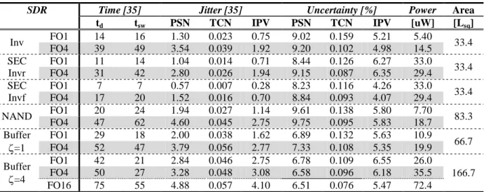
We performed transient simulations in SPECTRE using a 50% duty-cycle clock waveform as signal source and a single capacitance as load (CL). The clock slew-rate was configured to guarantee balanced transitions and the unit load chosen as the one that produces the same delay as the delay shown by an inverter at the middle of a long fanout-of-one inverter chain. Thus, the load can be configured as a multiple of the repeater’s input capacitance (CL=hCin), where h is the inverter’s fanout. Timing parameters were obtained, following their usual definitions: a) delay (td), was measured as the average of the time difference between input and output reaching 50% of Vdd, for rise (tr) and fall (tf) times; b) switching time (tsw), was measured as the average between tr,10/90 and tf,10/90; and c) absolute jitter (σtd), was obtained the standard deviation of the repeater’s delay, in the presence of Thermal Channel Noise (TCN), Power Supply Noise (PSN), Intra-die Process Variability (IPV) and temperature variations. To guarantee the clock signal’s integrity, we used Tclk = 20tsw.
TCN induced jitter was obtained using the transient noise simulation tool, available in Analog Design Environment (ADE) from Cadence. White noise samples are generated at each simulation step, with a variance determined by each transistor’s bias conditions. This results in time-dependent, zero mean, random noise current sources being considered in parallel with each transistor’s channel. Several parameters may be configured as described in Table 4. The configuration used in simulations is also shown and justified. Note that although TCN was scaled (10 times) to improve simulation accuracy, the results presented in this report were back-scaled to correspond to the actual repeater’s performance.
PSN induced jitter was evaluated with transient simulations using independent random Gaussian noise sources in power and ground rails (Mixed-Mode Noise - MMN). This guarantees that the repeater is equally affected by Differential Mode Noise ( DMN) and Common Mode Noise (CMN). Noise samples were generated in MATLAB and imported into SPECTRE as piece-wise linear voltage sources with configurable noise gain and step (Tn). In Fig. 17a, we show the impact of different PSN levels on jitter insertion, for a FO4 inverter with Tn=Tclk and Tn=4Tclk. It shows that jitter grows almost linearly with PSN standard deviation (σpsn) if it is small (< 10%Vdd), and exponentially if it is higher. Hereafter we will consider only small PSN levels, as it is the most common scenario in well designed Integrated Circuits (ICs). Thus, jitter can be considered to depend linearly on PSN magnitude, as is usually observed in practice [33]. In Fig. 17b, jitter is shown as a function of the noise cut-off frequency (fn=1/Tn). It shows a resonance peak for fn=fclk and again for fn=2fclk. In contrast, for fn<<fclk, jitter is almost constant. Because PSN is usually considered to have a low-frequency spectrum compared to the clock frequency, we will also hereafter assume fn=0.25fclk.
In general, the run length of a transient simulation depends on the system nature. In a terminating system, the duration of the simulation is fixed by specification or by an event definition that marks the end of the simulation. The simulation goal is to understand system
Table 4: Transient noise analysis: configuration parameters.
Parameter Description Value Justification
noisefmax
Bandwidth of pseudo random noise sources. A non-zero value turns on the noise sources during
transient analysis.
0.5 p (1)
This is the knee frequency for typical digital signal shapes, which is not too far beyond the inverter ’s intrinsic
-3dB bandwidth [32]. noisescale noise scale factor applied to all
generated noise. 10
This gain used to artificially inflate the small TCN and make it visible, above transient analysis numerical
noise floor. noiseseed Seed for the random number
generator. 1
We use the same seed across simulations, to compare the repeater
’s performances under the same circumstances.
noisefmin
Power spectral density (PSD) of noise sources depend on frequency in the interval from
noisefmin to noisefmax.
noisefmax (default)
In this case, only white noise is considered.
noisetmin Time interval between noise source updates.
1/noisefmax (default)
Smaller values would produce smoother noise signals, but would
reduce time integration step.
behaviour for a typical fixed duration. On the other hand, a non-terminating system is in perpetual operation and the goal is to understand its steady-state behaviour. In the present case, the system is non-terminating unless we specify an event to mark the end of simulation. If jitter could be calculated during the simulation run, the event could be the time instant for which a given confidence level was reached for the chosen performance metric. Unfortunately, absolute jitter can only be calculated after the simulation run and thus, a fixed simulation time (Tsim) had to be imposed. Because the accuracy of the sample standard deviation is directly proportional to sample size, we can only reach a reasonable value for Tsim by inspection of simulation results.
Figures 18a and 18b show the inverter’s TCN and PSN jitter evolution for growing sample sizes (N=Tsim/Tclk). Both have shown to follow inverse exponential functions towards a reasonable constant final value. However, PSN jitter took a much longer simulation time to do that. To have accurate results within a reasonable simulation time, the simulation run length was set to one thousand clock cycles for TCN jitter (N=1000) and three thousand for PSN jitter (N=3000). IPV jitter was evaluated with Monte Carlo (MC) simulations, which also usually requires thousands of simulation steps until enough delay values are obtained. Fortunately, screening experiments have shown that a reasonable number of runs could be used in such simple structures as clock repeaters. Fig. 18c shows IPV jitter in the reference repeater for an increasing number of runs and the correspondent simulation time penalty (simulation time compared to the time needed for 50 runs). A good compromise between accuracy and simulation time was found to be around 200 runs.
Jitter simulations results are shown in Fig. 19a for a balanced reference repeater, with σpsn=10%Vdd and increasing fanouts (FoN, N=1..6). Jitter is shown to increase linearly with fanout for all sources, but with different rates. For this fanout range TCN jitter increased 1.1
Fig. 17: PSN jitter in the reference FO4 inverter, for different: a) noise levels (σpsn/Vdd); and b) cut-off
times, while PSN and IPV jitter increased 3.2 times and 2.6 times, respectively. TCN jitter grows slowly with fanout because the high-frequency noise components are affected by the low-pass filtering imposed by CL. It is also shown to be much smaller (one order of magnitude) than PSN or IPV jitter. Yet, TCN jitter will not be neglected as it represents a fundamental limit on dynamic timing precision. On the contrary, PSN and IPV jitter have the same order of magnitude for σpsn10%Vdd.
Furthermore, to observe the impact of different noise modes, we repeated PSN jitter simulations using random noise sources in power and ground rails, in different configurations. Fig. 19b shows that jitter induced by CMN sources is higher than for DMN sources, while jitter induced by MMN sources (independent noise sources in power and ground rails) falls between CMN and DMN bounds. MMN jitter is around 35% lower than CMN jitter and 35% higher than Fig. 18: a) TCN jitter vs. N; b) PSN jitter vs. N; c) IPV jitter vs. MC runs. The elapsed simulation time
reference is the time taken to perform 50 runs (reference value).
Fig. 19: Jitter in the reference inverter, for different fanouts and: a) PSN, TCN and IPV sources; b) CMN,