Catarina Martins Rodrigues
Licenciada em Engenharia de Micro e Nanotecnologia
Spray Coating of Oxide and Chalcogenide
Semiconductor Layers for TFT Application
Dissertação para obtenção do Grau de Mestre em
Engenharia de Micro e Nanotecnologia
Orientador: Doutor Albert van Breemen, Investigador, Holst Centre
Co-orientador: Doutor Pedro Miguel Cândido Barquinha, Prof. Auxilar,
FCT/UNL
Júri:
Presidente: Doutora Rodrigo Ferrão de Paiva Martins, Prof. Catedrático Arguente: Doutora Rita Maria Mourão Salazar Branquinho, Prof. Auxiliar Convidada Vogal: Doutor Pedro Miguel Cândido Barquinha, Prof. Auxiliar
iii
Spray Coating of Oxide and Chalcogenide
Semiconductor Layers for TFT Application
© Catarina Martins Rodrigues
Faculdade de Ciências e Tecnologia
Universidade Nova de Lisboa
Spray Coating of Oxide and Chalcogenide Semiconductor Layers for TFT Applications
Copyright © Catarina Martins Rodrigues, Faculdade de Ciências e Tecnologia, Universidade
Nova de Lisboa.
v
ACKNOWLEDGEMENTS
After six months in the Netherlands, I have lost track of everyone that helped me throughout this journey. During this time aboard, I met and worked with incredible talented people, some of which I can call friends. The reported work would not be possible without the guidance and support of a large number of people. From these I would like to highlight and sincerely thank:
To Dr. Albert van Breemen, who supervise my day to day activities of my internship at the Holst Centre. For the guidance, time and patience you had, and for supporting me even when the experiments were not working as we expected. I simply can’t thank you enough.
To Prof. Pedro Barquinha, who contacted Holst Centre to explore the possibility of my research internship there. Thank you so much for giving me the right advise, even when the thought of doing my master thesis project in another country seemed frightening and overwhelming. Your support and guidance in the beginning, as well as throughout my time in Eindhoven and especially in the final weeks is invaluable to me.
To Dr. Ashutosh Tripathi and Dr. Esger Smits for all the technical support and ideas shared in the meetings. To Dr. Gerwin Gelick, the head of our group at Holst Centre, for challenging me to think bigger. To Dr. Brian Coob for welcoming me to the group on my first day and showing me around. To Wilco Keur from Philips, for helping me in first few weeks in the laboratory, and to everyone from Philips Research who shared with me a kind greeting every morning.
To TNO and the Holst Centre for supporting my project and allowing me to use their facilities.
To the group of interns from Holst Centre, with whom I shared my lunch breaks, but especially to Kevin Felter, for helping me in the laboratory and for discussing the problems I had during my research. Also, a special thanks to Daphné Lafond, for the amazing times we shared and for keeping me company during the busiest times. Despite the few months I had for that, I really enjoyed to meet you both. To my colleagues and friends from FCT/UNL, for accompanying me through this past five years, for
helping me grown as a person and as a professional, for your support and patience. I’m especially
grateful to Ricardo Ramos and Daniel Pereira, for being such good listeners and friends.
To João Serafim, for your guidance, patience, care, friendship and love, thank you for your invaluable advice (yes, I did listen to some of it).
To my brother and sister, for always welcoming me home with a hug.
vii
ABSTRACT
This work documents the deposition and optimization of semiconductor thin films using chemical spray coating technique (CSC) for application on thin-film transistors (TFTs), with a low-cost, simple method. CSC setup was implemented and explored for industrial application, within Holst Centre, an R&D center in the Netherlands. As zinc oxide had already been studied within the organization, it was used as a standard material in the initial experiments, obtaining typical mobility values of 0.14 cm2/(V.s) for
unpatterned TFTs. Then, oxide X layer characteristics were compared for films deposited with CSC at 40°C and spin-coating. The mobility of the spin-coated TFTs was 103 cm2/(V.s) higher, presumably due
to the lack of uniformity of spray-coated film at such low temperatures. Lastly, tin sulfide, a relatively unexplored material, was deposited by CSC in order to obtain functional TFTs and explore the device’s
potential for working as a phototransistor. Despite the low mobilities of the devices, a sensitive photodetector was made, showing drain current variation of nearly one order of magnitude under yellow light. CSC technique’s simplicity and versatility was confirmed, as three different semiconductors were
successfully implemented into functional devices.
ix
Resumo
Este trabalho documenta a deposição e otimização de filmes finos semicondutores utilizando a técnica química de spray-coating (CSC), para aplicação em transístores de filme fino (TFTs), com um método
simples de baixo custo. O sistema de CSC foi implementado e explorado para aplicação industrial, no Holst Centre, um centro de I&D na Holanda. Como o óxido de zinco tinha já sido estudado dentro da organização, foi utilizado como material padrão nas experiências iniciais, obtendo valores de mobilidade típicos para TFTs não-padronizados de 0,14 cm2/(V.s). Seguidamente, as características
da camada de óxido X foram comparadas para filmes depositados por CSC a 40°C e por spin-coating.
A mobilidade dos TFTs produzidos usando spin-coating foi 103 cm2/(V.s) mais elevada,
presumivelmente devido à irregularidade do filme produzido por spray-coating a temperaturas tão
baixas. Finalmente, sulfeto de estanho (SnS), um material relativamente pouco explorado, foi depositado por CSC para obter TFTs funcionais e explorar o potencial do dispositivo para trabalhar como um fototransistor. Apesar das baixas mobilidades dos dispositivos, um fotodetector sensível foi fabricado, mostrando variações de corrente de dreno de quase uma ordem de grandeza sob luz amarela. Confirma-se a simplicidade e versatilidade da técnica de CSC, sendo implementados com sucesso três diferentes semicondutores em dispositivos funcionais.
Palavras-Chave: spray-coating, transístores de filme fino, óxido de zinco, sulfato de estanho,
xi
LIST OF ABBREVIATIONS
CSC Chemical Spray-Coating
EDS Energy Dispersive x-ray Spectroscopy
FR Solution Flow-Rate
IR Infrared
LCD Liquid Crystal Display LED Light Emitting Diode
MOSFET Metal Oxide Semiconductor Field-Effect Transistor PVD Physical Vapor Deposition
R&D Research and Development SEM Scanning Electron Microscope
SS Subthreshold Swing
TFT Thin-Film Transistor
TNO Netherlands Organization for Applied Scientific Research
UV Ultraviolet
xiii
LIST OF SYMBOLS
µFE field-effect mobility (m2/(V.s)
µSAT saturation mobility (m2/(V.s)
CI dielectric capacitance per unit area (F/m2)
H nozzle height or distance between nozzle and substrate (cm) ID current between drain and source (A)
IG current between gate and source (A)
IOFF transistor off current (A)
ION transistor on current (A)
L channel length (µm)
t deposition time (s)
T substrate temperature during deposition (°C) VD voltage between drain and source (V)
VG voltage between gate and source (V)
VON turn-on voltage (V)
VT threshold voltage (V)
xiv
TABLE OF CONTENTS
1.
Motivation and objectives ... 1
2.
Introduction ... 3
2.1.
Spray Coating: A Cost-Effective Thin Film Deposition Technique ... 3
2.1.1.
Spray Coating vs Spin Coating ... 4
2.2.
Oxide Semiconductor Materials for TFT application ... 5
2.3.
Chalcogenides as High Performance Switching Materials ... 5
2.3.1.
Tin Sulfide ... 5
2.4.
Thin-Film Transistor: A Brief Overview of Device Characteristics ... 6
2.4.1.
Phototransistor: A Device for Light Detection ... 7
3.
Materials and Methods ... 9
3.1.
Precursor Solutions ... 9
3.2.
Substrates ... 9
3.3.
Thin Film Deposition Methods ... 10
3.4.
Characterization Methods ... 10
4.
Results and Discussion ... 13
4.1.
Zinc Oxide Standard Experiment: Spray Coating System Optimization ... 13
4.1.1.
Zinc Oxide Thin Films ... 13
4.1.2.
Thin-Film Transistor Considerations ... 13
4.1.3.
Zinc Oxide Thin Film Transistors ... 14
4.2.
Oxide X Deposited by Spin-Coating and Spray-Coating ... 16
4.2.1.
Oxide X Thin Film Optimization ... 16
4.2.2.
Oxide X TFTs: performance comparison between the two techniques ... 17
4.3.
Case Study: SnS Thin-Films ... 21
4.3.1.
SnS Thin-Film Optimization ... 21
4.3.2.
TFTs electrical measurements ... 23
4.3.3.
Phototransistor ... 25
5.
Conclusions ... 29
6.
Future Perspectives ... 31
xvi
LIST OF FIGURES
Figure 2.1
–
Schematic of a typical CSC setup, including possible components, adapted from
[1]. ... 4
Figure 2.2 - Characteristic curves of a TFT, with the output curves on the left and the transfer
curves on the right. Adapted from [62] and [63]. ... 7
Figure 3.1
–
Schematic of the TFT devices structure. A) Transversal view. B) Top view of a
ring transistor. The arrow represents the direction of current set for these devices throughout
the entire project. ... 9
Figure 3.2 - Implemented CSC system. A) Setup placed inside the fume hood: Power supply
for the mechanical rotation motor system (green), syringe pump (red), nozzle (yellow) and hot
plate (blue). B) Temperature controller device. ...10
Figure 4.1 - ZnO thin film characterization. A) Graph of thin film thickness (nm) dependence
on deposition time (s), showing a linear relation.
B) Profiles of three different films, with
deposition times of 20, 40 and 60 s, showing the roughness of the layers. ...13
Figure 4.2 - Schematic of the fringing electric field on unpatterned semiconductor layer of a
typical TFT arquitecture. Adapted from [73]. ...14
Figure 4.3
–
Electrical characterization of the ZnO TFTs. A) Transfer curves of ring transistors
with three different channel thicknesses. Continuous and dashed lines represent drain and
leakage currents, respectively. Arrows indicate the V
Gsweep direction, showing a clockwise
hysteresis. B) Output Curves of the ZnO TFT with film thickness of 15 nm. ...15
Figure 4.4
–
Optical images (on top) and film profiles (on the bottom) of oxide X samples
deposited using different nozzle heights, of 5, 7,9 and 11 cm, for samples I1, I2, I3 and I4,
respectively. ...17
Figure 4.5 - Optical images of oxide X films deposited on transistor substrates. A) Using
spray-coating with a fixed noozle height of 11 cm. B) Using spin-spray-coating. ...18
Figure 4.6 - Electrical characterization of the Oxide X TFTs with L of 40, 20 and 10 µm.
A)
Transfer curves of spray-coated TFTs.
B) Transfer curves of spin-coated TFTs.
Arrows
indicate the V
Gsweep direction, showing a clockwise hysteresis. ...18
Figure 4.7
–
Optical images (on top) and film profiles (on the bottom) of SnS samples
deposited using different nozzle heights, of 5, 7,9 and 11 cm, for samples I1, I2, I3 and I4,
respectively. ...22
xvii
showing a clockwise hysteresis. ...24
Figure 4.10
–
Comparison of transfer curves of spray-coated SnS TFTs with different channel
lenghts located on the same substrate, with T at 350 °C.
Arrows indicate the V
Gsweep
direction, showing a clockwise hysteresis. ...25
Figure 4.11 - Transfer curves of SnS TFTs before, during and after exposure to a yellow light
source.
A) Transistor with channel length of 40 µm. B) Transistor with channel length of 10
µm. Arrows indicate the V
Gsweep direction, showing a clockwise hysteresis in both TFTs. .26
Figure 4.12 - Transient Response of a SnS phototransistor when exposed to light. A) Cycles
of 20 seconds of light on and off. B) Analysis of a single cycle and consequent determination
of fall and rise times. ...26
Figure 4.13 - Response of Spray-Coated TFTs to Infrared Light. A) Transfer curves of a TFT
with L=40 µm before, during and after IR light exposure. Arrows indicate the V
Gsweep
xviii
LIST OF TABLES
Table 4.1
–
Extrated characteristic parameter values from Figure 4.3 of the produced ZnO
TFTs, considering different film deposition times (different thicknesses). ...15
Table 4.2
–
Extrated characteristic parameters from Figure 4.6 of Oxide X TFTs when
deposited by spin-coating and spray-coating, considering transistors with different channel
lengths. ...19
xx
LIST OF ANNEXES
Annex A - Prediction of the market demand for light sensors, where phototransistors can be
incorporated, showing an increasing demand over the next few years. ...39
Annex B
–
Alignment mask used for the contacts of the transistor substrates, where the
different transistor layouts can be seen. ...39
Annex C - Extraction method used for obtaining the characteristic parameters of the studied
TFTs. ...40
Annex D
–
Deposition parameters used for spray coating deposition of different samples of
oxide X thin films and respective optical images and film profiles. ...41
Annex E
–
Optical images of solutions with different solvents: A
–
Water; B- Isopropanol and
water in a 1:3 proportion; C
–
Isopropanol and water in a 3:1 proportion; D
–
Methanol. ...44
1
1. MOTIVATION AND OBJECTIVES
Although major research breakthroughs have been done in the past few years in the field of thin film deposition and its application to functional devices (such as thin-film transistors), most of physical vapor deposition (PVD) methods require the use of sophisticated and expensive instruments (namely vacuum pumps, electron beams or sputtering sources). Even though most PVD techniques present better film characteristics and, ultimately, better device performance, cheap chemical methods, such as the liquid phase chemical method spray coating (CSC), have been investigated for industrial applications and large scale deposition. These methods have attracted attention for their versatility (capability of achieving uniform layers of different materials) and throughput.
With this background in mind, this project was done for TNO and performed in the Holst Centre facilities, an independent R&D center located at the High Tech Campus Eindhoven, in the Netherlands. One of the goals of the organization is to provide functional, but simple solutions to industry, using as little resources as possible to achieve the projects’ goals. For that reason, this work was done using inexpensive, but effective characterization and production tools, such as optical microscopy and profilometry, which supported the decisions made to move forward with the project.
Even though the CSC technique has been widely explored by many research groups and its broad versatility proved by the successful deposition of a wide range of thin films, this technique was relatively new at the Holst Centre. So, this project was focused on the deposition and optimization of thin films, with the objective of precisely controlling its final characteristics (thickness, roughness, etc.) by simply changing parameters of the system. The optimized films were then deposited on silicon substrates containing an insulator layer and electrodes, in order to obtain a transistor structure (from now on called transistor substrates). By testing the device functionality, an assessment of the films’ quality could be made, in order to determine the technique’s viability in industrial processes.
In the first tests, zinc oxide (ZnO) was used as a standard semiconductor material to confirm the system was working properly. This oxide was chosen due to the availability of studies in the literature and also because a Holst Centre group had already worked with it for TFT applications. Then, a commercial solution developed and provided by a company’s partner was tested by request on the CSC system. The solution had been previously optimized for spin-coating technique, where a uniform oxide layer was deposited on a transistor structure and good, stable results were obtained. Since CSC is also a solution based deposition technique that requires less amount of material, the commercial solution was tested with this method and the results were compared to the spin-coated samples. For confidentiality reasons, the solution and material composition cannot be revealed. Therefore, the commercial solution and the
material’s layer will be presented as solution X and oxide X, respectively.
Lastly, a material that has not been explored for application in TFTs, tin sulfide (SnS), was studied as a semiconductor. This material has been previously researched for solar cell application, reveling high light absorption. So, the photodetection capabilities of the material were investigated by testing the produced TFTs to function as phototransistors.
Objectives
The project hereby described focus mainly on the CSC technique, as a cheap, scalable and easy to work with thin film deposition method. Functional thin-film transistors were produced and used as a proof of concept, showing that films with good properties can be deposited with the installed setup.
The main objective was to prove the technique’s versatility by using it to successfully deposit thin films of different materials, as a way to determine the viability of implementing it in the industry. This goal was accomplished in three different ways that show a different perspective of the project:
1) Implementation and optimization of the initial setup, by depositing ZnO thin films as a standard experiment and using them as a semiconductor layer on a functional transistor.
2
3) Case Study: Deposition of SnS layers aiming for the production of a functional device. The initial steps of an investigation of SnS to be used in a photodetecting device, such as a phototransistor, were performed.
3
2. INTRODUCTION
In this chapter, an introduction will be given on the relevant topics for the comprehension of the following chapters. As the developed work is based on the use of a simple, low-cost deposition technique, the CSC functionality will be described thoroughly. Then, previous studies on the semiconductor materials used will be presented, as well as a focus on the material deposited in the final case study, SnS. A direct, simple view of the functionality of a thin film transistor and its characteristic parameters will be presented. The chapter closes with a look into the final application proposed, the phototransistor. Throughout the project, the CSC will be defined as a deposition method where a liquid precursor solution is vaporized into an aerosol, reaching a substrate (that could be heated or not) and creating a layer on it, as the precursors react. This designation covers both spray deposition at ambient temperature and spray pyrolysis, where usually the substrates must be heated up to, at least, 100°C [1].
2.1. Spray Coating: A Cost-Effective Thin Film Deposition Technique
When choosing the deposition technique to be used for the production of a thin film, there are a number of options, which are often divided in two groups: physical vapor deposition (PVD) and chemical methods. In PVD a transfer of material is done from a reservoir to the substrate, by changing its physical state (ex.: sputtering, vacuum evaporation). In chemical methods which can be based on gas or liquid phase, a reaction between two components must occur for the film to form (ex.: chemical vapor deposition, spray pyrolysis) [1]. Nowadays, there is a constant pursuit from the semiconductor industry to discover and/or optimize ways for depositing thin films in a simple, cheap, large scale and quick way. Although PVD is often associated with better thin film quality, it needs expensive instruments and uses sophisticated processes to achieve them. Spray coating (a liquid phase chemical method) is able to answer all the above referred needs and still produce high quality layers of different materials.
CSC technique was first used to deposit thin films of CdS in 1966 [2]. Since then, several studies have been conducted on the deposition of different types of materials, such as metal oxides, single, binary and ternary chalcogenides or adamantine copper compounds. Virtually every material can be deposited by this technique, as long as a precursor salt is available [1], [3]. Also, thin films can be easily doped with the desired compound, by adding it to the precursor solution [4]. This technique has been used industrially in glass production and solar cells [5].
The reason this technique has attracted so much interest by researchers of different fields is its simplicity and low-cost processing, as it can be performed in ambient conditions (no vacuum systems required), using cheap equipment fairly easy to handle [3]. Even though no high quality substrates or precursors are required [6], good quality and uniform films can be obtained. The films’ final characteristics can be
easily controlled by changing the deposition parameters, making it possible to adapt the results to the desired application [4]. On the other hand, CSC setup could be scaled for large depositions, which is an essential characteristic for transitioning to industrial applications, where larger substrates are often used. However, CSC still faces some challenges. All the reactants must be able to coexist in the same solution, which also means they must be soluble in the same solvent. Differences in solubility can cause phase segregation for multicomponent materials [3], as the solution is not stable enough. Also, morphology of the film greatly depends on the parameters applied, which might be a problem considering the amount of variables involved.
A typical CSC system is composed of a set of components (see Figure 2.1):
Precursor solution dispenser, with a flow-rate controller device to precisely know the amount of solution used;
Nozzle, where the liquid solution is converted into an aerosol. There are different kinds of nozzles being used, such as air blast, ultrasonic and electrostatic [5]. The nozzle could also be associated with a mechanical apparatus that would move it according to specific patterns, designed to create a more uniform layer.
4
determined pressure is connected to it, in order to turn the liquid solution into an aerosol.
Hot plate, where the substrate is placed and can be heated, until the temperature required for the precursors to react and for the solvent to evaporate.
Thermocouple, used to measure the temperature of the hot plate. It is usually connected to a temperature controller, whose function is to keep the temperature at the desired levels.
Figure 2.1– Schematic of a typical CSC setup, including possible components, adapted from [1].
In the CSC process, a precursor solution and compressed inert air travel through a set of small tubes until they reach a nozzle, where the liquid is pulverized, so that it arrives to the substrate in the form of small droplets. The substrate could be heated to potentiate a chemical reaction, occurring between the solution’s constituents with the objective of forming a thin film of the desired compound. The temperature
of the hot plate is set, controlled and maintained by a thermocouple and a temperature controller. Every other product of the reaction should be volatile, so that it can be extracted (exhausted) from the deposition site [4].
Several parameters can be controlled in the system, such as substrate temperature, air pressure, solution flow-rate, precursor solution composition, deposition time, nozzle distance to substrate (its height) and nozzle positioning and/or motion, in order to obtain films with the specified characteristics. Of those, substrate temperature has been considered one of the most important parameters [6], as it influences solvent evaporation, droplet impact with consecutive spreading, and precursor decomposition [5], all essential processes in CSC. Substrate temperature can change the films’ characteristics, causing different optical and electrical behavior. Also, the compositional choice of the precursor solution plays an important role in the final product obtained, has the pH and the oxidation states of the salts chosen influence the structure and morphology of films [5]. Therefore, the effect of these factors must be taken into account when optimizing the thin film deposition of a new material.
2.1.1. Spray Coating vs Spin Coating
Spin-coating deposition method is also a liquid phase chemical deposition technique, based on the use of a precursor solution, such as CSC. Its functionality is based on the placement of the substrate in a rotating device. Drops of solution are put on top of the substrate, which is then set to rotate at a defined speed, for a determined time. The substrates are usually dried and heated after this process, to help evaporate the remaining solvent and enhance film formation [7].Therefore, it is also a simple and easy process to work with, like CSC, while achieving consistent results of thin and uniform layers.
5
industrial application. Since CSC does not present this kind of drawbacks, it is interesting to compare the quality of thin films obtained by these two techniques.
2.2. Oxide Semiconductor Materials for TFT application
Oxide semiconductor materials have been under the researchers’ focus for the past 10 years, as they provide the possibility of fully transparent applications, such as heat insulation films, solar cells and transparent displays [10]. Zinc oxide, tin oxide and indium oxide are among the most explored, due to their sufficiently large band gap (> 3.1 𝑒𝑉), high carrier density (> 1019 𝑐𝑚−3) and good mobility values (> 1 𝑐𝑚2/(𝑉. 𝑠)). However, even though these materials work properly as semiconductors, they can’t reach the conductivity values of conductors (up to 600,000 S cm-1 for copper), which presents itself has
an obstacle to the goal of designing fully transparent electronic devices [11].
ZnO is among the most explored oxide materials, with broadly available literature on its properties, production and applications [11]–[20]. ZnO films have been fabricated by several groups, using a number of different deposition technologies, such as sputtering [21]–[23], pulsed laser deposition [24]–
[26], chemical vapor deposition [27]–[29] and also solution based methods such as dip-coating [30], [31], spin-coating [32] and spray coating [33], [34]. The thin films are uniform and polycrystalline, and even though some of its processing methods do not require temperature, usually the substrate is subjected to heating during deposition or post-annealing. TFTs based on spray-coated ZnO present reported values of mobility between 0.2 and 15 cm2/(V.s) [35], [36].
2.3. Chalcogenides as High Performance Switching Materials
As the silicon-based electronic devices are more and more miniaturized, reaching the limit of Moore’s
Law, the scientific community started to seek for new materials. Graphene has attracted a lot of attention, as it is the strongest known material to date, it is stretchable, transparent, impermeable, and it has the highest intrinsic electron mobility ever registered, about 100 times the one of silicon [37]. However, it lacks a band gap, being unsuitable for digital electronic applications, as it cannot fully function as a semiconductor [38], or for solar cell applications [39], [40]. Without having this limitation, boron nitrites, metal chalcogenides, oxides, hydroxides and oxychlorides have all been explored as electronic materials. Of these kinds, chalcogenides have shown good promise, due to their high mobilities and air stability. Chalcogenides are composed of a transition element and a chalcogen (elements from group 16 of the periodic table) [38].
Molybdenum and tungsten based chalcogenides are the most studied for field-effect transistors (FET) application, presenting band gaps from the visible to the near-infrared [38]. When applied to FET structures, MoS2 based devices show mobilities in the order of 200 cm2/(V.s) and large on/off ratios
(~108) [41]. PbS has also been applied to TFTs, with mobilities in the order of 0.09 cm2/(V.s), when
deposited by chemical bath deposition [42]. Ti, Sn and Zr based chalcogenides are also indicated as promising semiconductors, but haven’t been much explored to this day [38].
2.3.1. Tin Sulfide
SnS compounds have recently attracted attention due to their promising applications in optoelectronics and photovoltaics. SnS presents a band gap on the order of 1.3 eV [43]. It has been reported to be p-type in thin film form [44], with a resistivity of 32.9 Ω.cm and an absorption coefficient of around 104 cm -1 [45]. The toxicity of other materials used in the photovoltaics field, such as Cd, and the scarcity of Te,
In and Ga (present, for instance, in CdTe and CuInGaS2), has motived a search for an alternative
earth-abundant, non-toxic and inexpensive material [45], [46]. Even though SnS responds to this demands and it is, theoretically, a good material to apply in solar cells due to its high absorption coefficient, the latest reports have not reported efficiencies higher than 3.88% [47]. Nevertheless, SnS is a relatively unexplored material, so there is still much room for improvement and discovery of new applications for this semiconductor.
6
groups, where the effect of growth temperature and the tin and sulfur precursors ratio in the initial solution is reported [43]–[45], [48]–[54]. Usually stannous chloride (SnCl2) is used as a tin precursor and
thiourea (CS(NH2)2) as a sulfur precursor, even though SnCl4 and variations of substituted thiourea have
been tried (such as N,N – diethyl or N,N – dimethyl thiourea). As solvent, water is the most used. The substrate temperature was reported as the most influential parameter in SnS spray coating, since
it greatly affects the films’ phase composition, an important property, as each phase has different characteristics. It has been reported that tin monosulfide (SnS) can be achieved at temperatures between 300 and 375°C, being 350°C the temperature at which the film is SnS abundant. The precursor ratio has also been reported to influence the phase composition. While most studies use the 1:1 ratio, Sajeesh et al. [52] have tested solutions with 1:1, 1:2, 1:3 and 1:4 ratios at different temperatures, concluding that the 1:2 ratio solution produced the most stoichiometric solutions for T=350°C, possibly due to sulfur evaporation potentiated by the substrate temperature.
Even though the application of SnS in functional devices, such as TFTs, is still relatively unexplored, spin-coated p-type SnS films photocurrent response was recently studied, where a clear response to incident light is recorded [55]. Also, some reports on SnS2, another phase of tin sulfide, have recently
came out. U. Zschieschang et al. studied TFTs based on SnS2 deposited by chemical vapor transport,
achieving mobility values of 0.04 cm2/(V.s) and on/off ratios close to 106 [56]. SnS2 in the form of a single
layer obtained by mechanical exfoliation was applied as a semiconductor in a TFT structure by D. De et al., presenting high mobilities up to 1 cm2/(V.s) and on/off ratios in the order of 106 [57]. Photo detection
capabilities were also checked by Y. Huang et al. group, showing efficient phototransistor behavior, even though the response time to pulsed radiation could be improved [58]. Even though other similar studies on SnS2 are available in the literature [59], [60], studies on SnS are still limited, leaving much
room for further improvements.
2.4. Thin-Film Transistor: A Brief Overview of Device Characteristics
Thin-film transistors are field-effect devices working as switches and amplifiers, used in digital and analog electronics, especially flat panel displays. The field effect device was first described in the 30s in a patent by Lilienfeld, which was followed by Heil’s and Shockley’s, who described in more detail the operation and structure of the devices [61]. TFT technology was applied into a working device based on CdS in the 60s, but its research was laid aside due to the increasing interest in the Metal Oxide Semiconductor Field Effect Transistor (MOSFET) technology. It was only in the end of the 70s, with the study of amorphous silicon on TFTs to be applied as switches in LCDs, that subsequent investment in this field of research was done [61]. Recently, transparent, flexible and/or stretchable electronics are being explored, with the introduction of oxides and organics as semiconductors, aiming for wearable gadgets and smart applications.
TFTs are fabricated using thin layers of material and follow the same working principle as MOSFETs. It also has three terminals (gate, source and drain), where the drain and source electrodes are connected to the semiconductor layer, which is isolated from the third terminal, the gate, by a dielectric. The basic operation principle of the TFT is gate modulation of the current flowing between drain and source, which determines if the transistor is on or off [62]. The TFT can be fabricated in different configurations according to the place where the layers and terminals are: they can be top-gate or bottom-gate, and, among these, staggered or coplanar. The choice of configuration is based on the fabrication requirements and the final application. Also, depending on the type of polarity, n-type or p-type, and the value of the threshold voltage, VT, the TFT can also be classified in enhancement or depletion mode
devices: for an n-type device VT is positive or negative, respectively, the opposite applies for p-type
transistors [63].
TFTs can be working in one of the following three states:
OFF State, if the drain voltage is zero, 𝑉𝐷 = 0𝑉, as negligible current is flowing between drain and source, 𝐼𝐷, regardless of the gate voltage, 𝑉𝐺;
7
𝐼𝐷 = 𝐶𝑖 𝜇𝐹𝐸 𝑊𝐿 [(𝑉𝐺− 𝑉𝑇) 𝑉𝐷 −12 𝑉𝐷2] [2.1]
Where 𝐶𝑖 is the dielectric capacitance per unit area, 𝜇𝐹𝐸 is the field-effect mobility, W and L are the width and length of the semiconductor channel, respectively, 𝑉𝐺 is the gate voltage and 𝑉𝑇 is the threshold voltage. When VD<<0 V, the quadratic term of the equation can be neglected, resulting in a linear relation
between 𝐼𝐷 and 𝑉𝐷, as a result of a uniform distribution of charges across the channel.
Saturation, if 𝑉𝐷 > 0𝑉 𝑎𝑛𝑑 𝑉𝐷 > 𝑉𝐺− 𝑉𝑇, in which case 𝐼𝐷can be defined by
𝐼𝐷 = 𝐶𝑖𝜇𝑠𝑎𝑡2𝐿𝑊(𝑉𝐺− 𝑉𝑡)2 [2.2] Where 𝜇𝑠𝑎𝑡 is the saturation mobility. When approaching the 𝑉𝐷 = 𝑉𝐺− 𝑉𝑇 point, the semiconductor channel depth decreases near the drain terminal, increasing the channel resistance, which is usually called the pinch-off point. After this point, 𝐼𝐷 is no longer dependent on 𝑉𝐷 and eventually stabilizes (saturation).
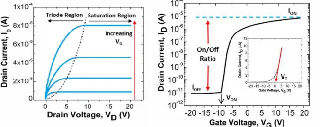
These operation modes are usually described using characteristic curves (see Figure 2.2), such as output and transfer curves. Several characteristic parameters can be taken from these curves, like the ratio between on- and off-current, VT, VON, mobility (either field-effect or saturation) and the subthreshold
swing (SS) [64].
Figure 2.2 - Characteristic curves of a TFT, with the output curves on the left and the transfer curves on the right. Adapted from [65] and [63].
2.4.1. Phototransistor: A Device for Light Detection
As one of the chosen semiconductors was photosensitive, a phototransistor was fabricated in this project. The invention of these devices is often attributed to John N. Shive of Bells Labs [66]–[68], shortly after the first transistors were invented during the late 1940s, using a germanium point-contact transistor. Even though the first application tested was its integration in a component of the telephone, the phototransistor would eventually emerge as a television and video-imaging technology[68].
A phototransistor is a three-terminal switching device that relays on the exposure to light to operate, which causes variations of current that can be measured. Photodetection occurs due to the photogenerated carriers that are formed when the energy of a photon is equal or higher than the
8
9
3. MATERIALS AND METHODS
In this section, a detailed description of the solutions, substrates, equipment and techniques used to deposit films, characterize and test them on devices is made.
3.1. Precursor Solutions
A 0.1M solution of zinc acetate (Zn(CH3COO)2 - Sigma Aldrich with 99.99% purity) dissolved in methanol
(CH4O) was used for deposition of the ZnO films.
Solution X was used to deposit Oxide X. The concentration of the solution was controlled by adding solvent provided by the manufacturer of Solution X. It was considered that the volumetric density of Solution X and Solvent X were the same.
For the deposition of SnS, a mix of two precursor solutions was made. Firstly, a 0.1M of tin (II) chloride dehydrate (SnCl2 .2H2O - Sigma Aldrich with 99.99% purity) solution was made by dissolving the salts
in methanol. As the SnCl2 . 2H2O salt dissolved tends to form a precipitate (SnCl2 (aq) + H2O (l)
Sn(OH)Cl (s) + HCl (aq)), a few drops of HCl were added to prevent this effect. Secondly, thiourea (CH4N2S - Merk with a 99% purity) was dissolved into methanol in order to obtain a concentration of
0.2M. A volume of 10 mL was prepared for both solutions and they were both kept stirring until the salts were completely dissolved. Finally, the solutions were mixed (10 mL of each) and stirred, making the final mix ready for application.
3.2. Substrates
P-type silicon wafers with a {111} crystal orientation coated with photoresist were used for film optimization tests. The wafers supplied were cut into individual pieces of 1.75x1.75 cm. The layer of photoresist worked as a protective layer, keeping the samples as clean as possible. So, prior to sample use, the photoresist was removed from each individual sample, using acetone and isopropanol. To
enhance the substrate’s cleanness, the samples were placed on a UV/Ozone PhotoReactor (model PR-100 from UVP.inc) for 5 minutes.
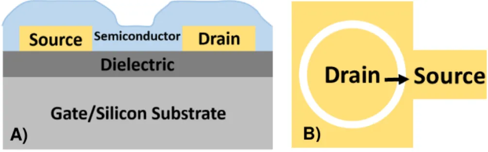
For the TFT testing, pre-made commercial n-type Si substrates with a {111} crystal orientation were used. The wafers supplied were cut into individual pieces of 1.75x1.75 cm. The substrates contained a 210 nm SiO2 layer as dielectric across in the entire wafer. The S/D electrode layers consisted of a 2 nm
Ti layer on the bottom (for enhanced adhesion) and 50 nm layer of gold on top, defined by conventional photolithography, using the mask that can be consulted in Annex B. The substrates were supplied already with those layers deposited, so the semiconductor layer was deposited on top. A lateral view of the device structure can be seen in Figure 3.1. Although the used mask allowed the choice among different transistor configurations, after the initial experiments, the chosen layout was the ring transistor, yielding TFTs with W of 1000 µm and L ranging between 10 µm and 40 µm. The current was set to run from the inner electrode to the outer electrode (as can be seen in Figure 3.1). The referred choices will be explained in section 4.1.2.
Figure 3.1– Schematic of the TFT devices structure. A) Transversal view. B) Top view of a ring transistor. The
arrow represents the direction of current set for these devices throughout the entire project.
10
3.3. Thin Film Deposition Methods
The main focus of this thesis was the implementation and optimization of a CSC system (Figure 3.2). Even though it was homemade, most of its components had already been used in previous work, reported by Andringa et al. [73]. Modifications in the precursor solution dispenser were made to ensure a controlled flow-rate and to study its influence. This comprised storing the solution in a syringe during deposition, to prevent solvent evaporation, and installing a syringe pump to precisely control the amount of sprayed solution. However, at the beginning and end of deposition, the FR seemed to be irregular (discontinuous spraying). So, an improvised shutter (placed between the nozzle and the substrate), consisting on a glass barrier attached to a universal support, was implemented. All the other instruments (heater, thermocouple, nozzle, rotational mechanical motor and air pressure controller) had already been used in the previous experiment mentioned above.
The chosen nozzle (a Meinhard Nebulizer TR-30-A3) was connected to a nitrogen air flow at a constant pressure of 1 bar and to the syringe pump (Havard Apparatus 11plus), from where the solution was injected at a determined flow rate (FR), ranging between 0.1 and 3 mL/min. The nozzle’s mechanical rotation motor system (Maxon) and powered by a power supply (Delta Electronika) at a constant voltage of 1 V, was implemented to ensure better uniformity of films, which kept the rotation speed and radius constant throughout the experiments. The substrates were placed on a heater (Ceran 500 11A controlled by a Eurotherm system), maintained at constant temperature (T), ranging between 30 and 400°C, depending on the experiment (± 5ºC). Nozzle height (H) values were varied between 5 and 11 cm and deposition time (t) between 15 and 120 s. The specific parameters used for each experiment will be stated in the respective results section.
Figure 3.2 - Implemented CSC system. A) Setup placed inside the fume hood: Power supply for the mechanical
rotation motor system (green), syringe pump (red), nozzle (yellow) and hot plate (blue). B) Temperature controller
device.
For spin-coating deposition, a ATMsse OPTIspin SB20 spin coater system was used to make the standard layers and devices. The rotation speed was maintained at 3000 rpm and time the time at 30 s, according to previous tests made by a Holst Centre team.
3.4. Characterization Methods
Film thickness and roughness in layers deposited onto Si substrates were measured by a DektakXT profilometer, equipped with a 12.2 µm tip. The samples were scratched with a surgical blade and the step between the scratch and the film was measured in order to determine the films’ thickness. Although this technique proved to be sufficient with film thickness higher than 20 nm, for thinner films the scratches were not very well defined, making it impossible to accurately do the measurements. Optical observation and image caption was done with a Leica Microscope.
Scanning electron microscopy (SEM) was used for evaluation of the surface morphology of SnS films, using a Zeiss Auriga crossbeam. Given the reduced thickness of the films a low accelerating voltage was used (1 keV), together with in-lens secondary electrons detector. Elemental analysis of the same
11
films was obtained by energy dispersive X-ray spectroscopy (EDS) using a Oxford XMax-150 detector (inside Zeiss Auriga) with AZTec software. Analysis was carried out using accelerating voltage of 15 keV and aperture size of 60 µm to assure good compromise between x-ray signal and spatial resolution. For the electrical characterization of the TFT substrates, consisting of transfer and output characteristics, Hewlett Packard 4155B Semiconductor parameter analyzers was used, with Cascade Microtech M150 manual probe stations, placed inside a glove box from MBraun (MB 200B), where the atmosphere was controlled, preventing the presence of oxygen or water in the air. To extract and analyze the data, Agilent Desktop Easy Expert software was used.
13
4. RESULTS AND DISCUSSION
4.1. Zinc Oxide Standard Experiment: Spray Coating System Optimization
As previously mentioned in section 1, the CSC technique was relatively new in the Holst Centre. So, before the start of the project, it was necessary to assemble and test the system to ensure its functionality. Also, some changes had to be implemented, to maximize the quality of the final thin films. For controlled flow rates and precise deposition times, a syringe pump and a shutter were added.
4.1.1. Zinc Oxide Thin Films
ZnO thin films were chosen as a standard experiment due to the availability of reports found in literature and also because a similar study had been conducted previously in the Holst Centre, with the goal of achieving a NO2 gas sensing device [73]. Most of the deposition conditions, such as the temperature of
400°C, the precursor solution (0.1M of zinc acetate in methanol) and the deposition time (1 minute), were established based on that project. However, some parameters had to be experimented and optimized. To study the FR, the nitrogen pressure was set to 1 bar and the H to 5 cm. Different values were tested (0.1, 0.2, 0.5 and 1 mL/min), keeping the deposition time at 1 minute, with the objective of getting even and good quality films. Smaller FR of 0.1 and 0.2 mL/min produced very thin films for the fixed t of 1 minute, going against the objective of high throughput, necessary for industrial applications and, therefore, intended for these experiments. On the other hand, roughness in films deposited using 1 mL/min of FR was higher. So, an intermediate value of 0.5 mL/min was used to obtain uniform films and high throughput, achieving film thicknesses of 40 nm.
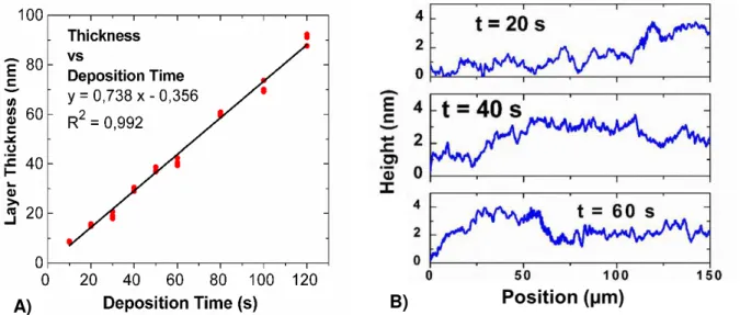
Then, the deposition time was varied in order to study its influence on the films’ quality. A thickness analysis to the films was performed, achieving values between 10 and 90 nm, for t below 120 s. A linear relation between deposition time and film thickness can be made, as seen in Figure 4.1 A. Knowing this relation, it is possible to estimate the layer thickness by choosing a specific deposition time. Also, very uniform structures were obtained, as can be seen by the profiles of Figure 4.1 B, where the roughness is not higher than a few nanometers. These results confirm the possibility of this system to obtain very uniform semiconductor layers and precisely controlled film thicknesses with ZnO.
Figure 4.1 - ZnO thin film characterization. A) Graph of thin film thickness (nm) dependence on deposition time (s),
showing a linear relation. B) Profiles of three different films, with deposition times of 20, 40 and 60 s, showing the
roughness of the layers.
4.1.2. Thin-Film Transistor Considerations
Over the current study, the semiconductor layer deposited by the CSC technique of the fabricated TFTs was never patterned, for improved throughput. Even though this model of research is suitable for initial
14
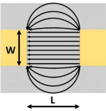
studies, it can also lead to some problems, such as overestimation of field-effect mobility due to fringing electric fields. This effect is reflected on an actual increase of the semiconductor dimensions, namely a larger transistor width than the one geometrically defined by the width of source-drain electrodes, due to peripheral currents (also called fringing currents) [74] (Figure 4.2).
Figure 4.2 - Schematic of the fringing electric field on unpatterned semiconductor layer of a typical TFT arquitecture.
Adapted from [75].
Given this and since the transistor masks available allowed for the choice of different device layouts (as can be seen in Annex B), ring transistors were selected, as they provide a coaxial source-drain layout. This configuration prevents the fringing effect from happening, as long as the current is flowing from the inner contact circle (drain) to the outer contact circle (source) [75]. The same characteristic equations described in section 2 were used, as the device was considered to work similarly to a transistor in a common layout (as seen in Figure 4.2).
Also, as the gate electrode was the silicon substrate itself and due to the non-patterned semiconductor, an important effect of gate modulation, not only between drain and source (as intended), but across the substrate must be taken into account when analyzing TFT characteristics. On the other hand, high drain voltages were used to avoid gate leakage current exceeding drain-to-source current for larger gate voltages, an effect registered in the initial tests, when low drain voltages were applied. Hence, mobility values were estimated using the saturation mode equations (see Annex C for a detailed explanation).
4.1.3. Zinc Oxide Thin Film Transistors
When depositing the optimized thin films (as described in section 4.1.1, with T of 400 °C, FR of 0.5 mL/min and H of 5 cm) on transistor substrates and then annealing them inside the glove box for 30 minutes at 250°C. Transistors with fixed channel lengths of 10 µm and layers with different thicknesses of semiconductor were analyzed, from which the transfer and output curves seen in Figure 4.3 were obtained.
Even though all the analyzed ZnO thicknesses provide noticeable field effect, thinner layers result in lower off-current and VON closer to 0 V, suggesting an increase in electrical resistivity of the material
(see also Table 4.1). This effect might be explained by the typically smaller grain sizes in thinner ZnO films (considering a columnar growth structure) and/or that the amorphous incubation layer is present in most of the films depth, factors that make the carrier transport more difficult. Note that, while the trend of SS with thickness seems to suggest improved interface properties for thinner films, an opposite trend is verified for µSAT. So, it should be considered that SS is significantly degraded by the larger off-current
of thicker films.
Even though the µSAT values are quite small when compared to some research group’s work, such as
Fortunato et al., where mobilities of 20 cm2/(V.s) have been achieved on sputtered ZnO TFTs [35], it is
15
depositions made on a substrate heated to 400 °C. This effect is attributed to the energy offset between the Fermi level of Au (EF = 5.1 eV) and the band gap of ZnO (4.4 eV), as the Fermi level of Al allows for
a smaller energy offset (4.2 eV), and also to the different device arquitectures.
Therefore, the low mobility values of Table 4.1 could be explained not only by the solution based technique used, but also by the choice of TFT arquitecture, electrode and dielectric (which should be optimized for each device, considering the semiconductor chosen).
Figure 4.3– Electrical characterization of the ZnO TFTs. A) Transfer curves of ring transistors with three different
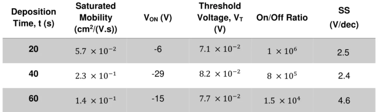
channel thicknesses. Continuous and dashed lines represent drain and leakage currents, respectively. Arrows indicate the VG sweep direction, showing a clockwise hysteresis. B) Output Curves of a TFT with films of 15 nm. Table 4.1 – Extrated characteristic parameter values from Figure 4.3 of the produced ZnO TFTs, considering
different film deposition times (different thicknesses).
Deposition Time, t (s)
Saturated Mobility (cm2/(V.s))
VON (V)
Threshold Voltage, VT
(V)
On/Off Ratio SS (V/dec)
20 5.7 × 10⁻² -6 7.1 × 10⁻²
1 × 10⁶ 2.5
40 2.3 × 10⁻¹ -29 8.2 × 10⁻²
8 × 10⁵ 2.4
60 1.4 × 10⁻¹ -15 7.7 × 10⁻²
1.5 × 10⁴ 4.6
In light of the results obtained and of the considerations made, the technique’s setup was considered
capable of producing uniform and good quality thin films. With these results in mind and knowing the limitations of the methodology employed, the project moved forward to the main experiments, with other materials. This standard experiment was later on performed again every time the results suggested system malfunction in order to confirm its reliability.
16
4.2. Oxide X Deposited by Spin-Coating and Spray-Coating
In this section, a comparison of two methods for deposition of thin layers, spray coating and spin coating, is presented, while employing the same precursor solution, solution X, to get oxide X semiconductor film. The objective of this experiment was to provide information to a Holst Centre partner about the applications of a commercial solution that had been developed at the time for spin-coating, by assessing if it was suitable for spray-coating deposition. One of the requirements of the partner for this project was the use of substrate temperature while spray-coating below 100°C.
After deposition, every thin film was annealed two times, according to the procedure developed for spin-coated films. The first one, a soft-annealing, was performed at 250 °C for 30 minutes, while the second, a hard-annealing, was done at 350 °C for 1 hour. These annealing procedures were done to mimic the conditions of the substrates produced by deposition of the two different techniques, so that they could be easily compared. The transistor substrates were also subjected to a 10 minutes UV curing, done
before the two annealing steps, in order to improve the material’s conductivity.
4.2.1. Oxide X Thin Film Optimization
Knowing this material had never been deposited by CSC technique and considering it is an oxide, the first tests were based on the experience acquired from the section 4.1.1. The goal at this stage was, by applying different processing conditions and analyzing the optical images and profiles of the samples deposited on Si, to reach an optimal set of parameters that would result on the deposition of homogenous films. After each attempt, an optical image and the profile of the sample were taken to determine if the experiments were moving forward in the right direction, as can be seen in Annex D. From now on, samples will be named using their respective serial number.
Since the solution was firstly optimized for spin-coating, the first assumption made was that it might be too concentrated for spray-coating, so in the initial tests low flows (0.1 mL/min) and low deposition times (15 and 30 seconds) were used. Also, a near-ambient substrate temperature of 40°C for deposition was chosen to match spin-coating conditions, while keeping H at 5 cm. A1 images and profiles show that this set of parameters results on the formation of material accumulations, which are intensified with the increase in deposition time, as seen in A2 (see Annex D).
Since increase in temperature generally causes an improvement of film uniformity, the goal of the second set of samples (B1, B2, B3) was to study the substrate deposition temperature effect on the films ( T of 40, 60 and 80°C were used). Also, in an attempt to redistribute the material accumulations throughout the film, the FR was increased to 0.5 mL/min. However, this approach caused even higher irregularities and uneven films, as can be seen by the material peak of 3500 nm height present in the profile of B3.
The third set of samples was made returning to near-ambient temperatures (40°C) and diluting the initial solution used, mixing one part of Solution X and three parts of solvent (1:3 solution). The most uniform sample seemed to be C2, but, when repeating the deposition under the same conditions, irregular films were obtained, showing important issues of reproducibility.
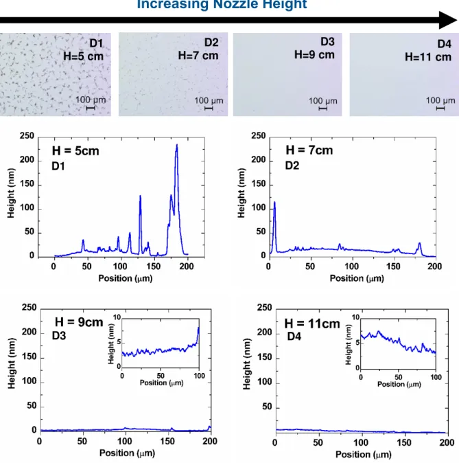
After trying different combinations of parameters without success, the nozzle height influence was tested on Set D, keeping near-ambient T of 40°C, FR of 0.1 mL/min, t of 20 seconds and using the 1:3 solution. As can be verified by the optical images and profiles of Figure 4.4, the films uniformity seems to improve as the height increases. Irregularities of the sample with H=5 cm are visible and reach about 200 nm of height. These values drastically decrease when H is set to 11 cm, for which the irregularities can no longer be seen in the sample, as confirmed by its profile (height differences of less than 5 nm). This effect might be explained by the smaller droplet size of the spraying at the substrate level for higher H, resulting in a uniform material distribution on the substrate.
17
only caused the reappearance of irregularities in the film, thus the deposition time was kept at 20 seconds for future depositions and H at 11 cm to guarantee the most uniform layers possible. Film presence was later on confirmed with transistor structures as explained in the next section.
Figure 4.4– Optical images (on top) and film profiles (on the bottom) of oxide X samples deposited using different
nozzle heights, of 5, 7,9 and 11 cm, for samples I1, I2, I3 and I4, respectively.
4.2.2. Oxide X TFTs: performance comparison between the two techniques
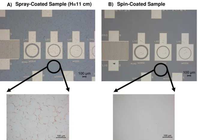
The previously optimized spray-coated Oxide X D4 thin films (H=11 cm) where deposited on transistor substrates, in order to confirm the films’ presence and compare, by analyzing the TFT behavior, spin-coated and spray-spin-coated films. It is necessary to consider that the spin-coating deposition of the Solution X had already been optimized by another Holst Centre team (see parameters in section 3.3). No changes were made to the processing by this technique, as the main focus was the CSC. As can be seen in Figure 4.5, silicon dioxide below the spray-coated Oxide X enhances the presence of coffee-ring structures, probably shaped according to the size of the spray’s droplets and by the slow solvent evaporation, happening due to the low substrate deposition temperature used. The film made with spin-coating does not show this effect, looking uniform and free of film irregularities.Increasing Nozzle Height
D1
H=5 cm
D2
H=7 cm
D3
H=9 cm
H=11 cm
D4
D1
D2
18
Spray-Coated Sample (H=11 cm)
Spin-Coated Sample
Figure 4.5 - Optical images of oxide X films deposited on transistor substrates. A) Using spray-coating with a fixed
noozle height of 11 cm. B) Using spin-coating.
When extracting the TFTs transfer curves (Figure 4.6), a clear confirmation of the presence of Oxide X layer on the transistor substrates can be drawn. Therefore, the spray-coated Oxide X thin films can be applied as semiconductor layers of TFTs, producing functional devices.
Figure 4.6 - Electrical characterization of the Oxide X TFTs with L of 40, 20 and 10 µm. A) Transfer curves of spray-coated TFTs. B) Transfer curves of spin-coated TFTs.Arrows indicate the VG sweep direction, showing a clockwise
hysteresis.
A)
B)
19
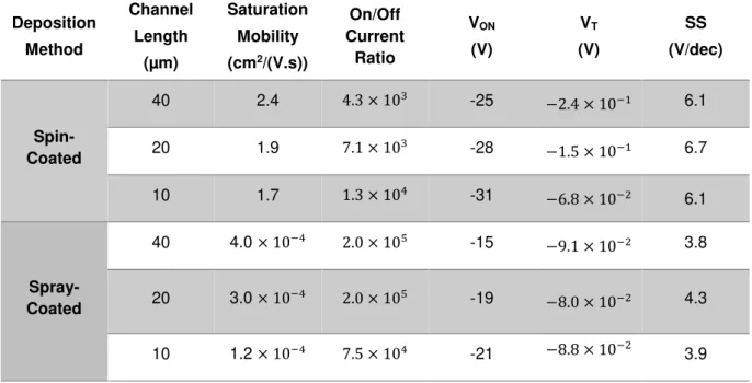
Very different results can be observed in both graphs, explained by the lower on and off currents present in spray-coated TFTs, which leads to lower mobility values and overall inferior results (Table 4.2).
Table 4.2– Extrated characteristic parameters from Figure 4.6 of Oxide X TFTs when deposited by spin-coating and spray-coating, considering transistors with different channel lengths.
Deposition Method Channel Length (µm) Saturation Mobility (cm2/(V.s))
On/Off Current Ratio VON (V) VT (V) SS (V/dec) Spin-Coated
40 2.4 4.3 × 10³ -25
−2.4 × 10⁻¹ 6.1
20 1.9 7.1 × 10³ -28
−1.5 × 10⁻¹ 6.7
10 1.7 1.3 × 10⁴ -31
−6.8 × 10⁻² 6.1
Spray-Coated
40 4.0 × 10⁻⁴ 2.0 × 10⁵ -15
−9.1 × 10⁻² 3.8
20 3.0 × 10⁻⁴ 2.0 × 10⁵ -19
−8.0 × 10⁻² 4.3
10 1.2 × 10⁻⁴ 7.5 × 10⁴ -21 −8.8 × 10⁻² 3.9
As the composition of this oxide semiconductor layer is unknown, generic reviews among the oxide based TFTs were consulted, in order to perform a critical analysis of the exposed results. Frenzel et al. review on transparent TFTs (where oxides are used as channel materials) explores the published work on this field of research between 2003 and 2013, considering different semiconductor deposition techniques and different device structures [76]. According to the compiled data, mobilities of oxide based TFTs are reported to be between 0.02 and 107.8 cm2/(V.s), with on/off ratios lying in the range of 101
-109 with subthreshold swings (SS) of 80-4000 mV/dec, depending on material selection, deposition
technique, (post-)processing parameters and device structure, showing a broad range of performance variation among this technology.
Fortunato et al. group collected information related to solution-processed oxides, including deposition techniques, such as spin-coating and spray-coating of different materials, for articles published until 2011 [77]. In the case of TFTs based on spin-coated ZTO, mobilities reported range from 0.76 and 27.3 cm2/(V.s), while the on/off ratios lay between 105 and 108. Spin-coated GIZO TFTs present mobilities
between 0.05 and 7.65 cm2/(V.s) with on/off ratios in the range of 104-107. Generally, it is observed that
solution-processed TFTs reveal lower mobility values when compared to devices with thin films processed by PVD.
The results obtained in this work follow this trend, achieving performance levels closer to the ones typically found for solution processed oxide TFTs. The coffee-ring topography verified in Figure 4.5 for spray-coated films should be the main responsible for degraded performance when comparing to spin-coated devices, as this creates areas of film with different thickness that interfere with the movement of carriers across the channel layer, due to a larger defect concentration, increasing its electrical resistivity. This is reinforced by the fact that both mobility and off-current are significantly higher for spin-coated TFTs, explained by the device’s sensitivity to the electrical resistivity of the semiconductor layer, due to
the gate modulation of a large area of the devices and not only between drain and source electrodes (see section 4.1.2).
The effect of L on device properties also reinforces the improved layer uniformity of spin-coated films. As would be expected from equation 2.2, maximum ID should scale with W/L, unless layer uniformity,
20
spin-coated samples only a small effect of contact resistance for shorter channel devices is notorious by the small degradation of µSAT as L decreases. This effect should not be attributed to overestimation
of µSAT for longer L, since the ring transistor layout used in this work inhibits fringing current effects, as
mentioned in 4.1.2. Still, maximum ID scales almost perfectly with W/L. On the other hand, for
spray-coated samples the evolution of ID with W/L does not appear to follow the same trend, which should be
due to the large degree of non-uniformity of the semiconductor films.
Results in Table 4.2 can also be compared with the ones presented in table 4.1, for sprayed ZnO TFTs. Data shows that significantly improved field-effect modulation is achieved with ZnO than with oxide X. In addition to the effects of resistivity and film uniformity mentioned above in the comparison of spin-coated and spray-spin-coated samples, the effect of film thickness should also be highly relevant here. Since it was not possible to accurately determine the thickness of oxide X, results suggest that it should be very low (below 15 nm), possibly even compromising the continuity of the film through all the area between source and drain electrodes, inhibiting significant current modulation with moderate values of VG.
![Figure 2.1 – Schematic of a typical CSC setup, including possible components, adapted from [1]](https://thumb-eu.123doks.com/thumbv2/123dok_br/16694680.743775/24.892.178.718.187.513/figure-schematic-typical-setup-including-possible-components-adapted.webp)