Towards printed carbon nanotube transistors on paper
substrates
Dissertação para obtenção do Grau de Mestre em
Engenharia de Micro e Nanotecnologia
Gonçalo José Pena Rodrigues
Licenciado em Engenharia de Micro e Nanotecnologia
Orientador:
Luís Pereira, Professor auxiliar, Faculdade de
Ciências e Tecnologia
–
Universidade Nova de
Lisboa
Co-orientador:
Pawel Wojcik, Investigador CEMOP/UNINOVA,
Faculdade de Ciências e Tecnologia
–
Universidade
Nova de Lisboa
Júri:
Presidente: [Prof. Dr. Rodrigo Ferrão Martins] Vogal: [Prof. Dr. Luís Miguel Pereira] Vogal: [Prof. Dr. Fernando Jorge da Cruz]
TOWARDS PRINTED CARBON NANOTUBE
TRANSIS-TORS ON PAPER SUBSTRATES
© Gonçalo José Pena Rodrigues
Faculdade de Ciências e Tecnologia
Universidade Nova de Lisboa
Towards printed carbon nanotube transistors on paper substrates
Copyright © Gonçalo José Pena Rodrigues, Faculdade de Ciências e Tecnologia, Universidade Nova de Lisboa.
i
Acknowledgments
This work was only possible thanks to several people, who helped me a lot with all I needed during the whole thesis.
To Professor Luís Pereira, thank you for your availability to help me and the guidance that you gave me when work seemed to be stuck.
To Pawel Wojcik for the support on all the question that I had related to inkjet printing.
To Professor Rodrigo Martins and Professor Elvira Fortunato, thank you for giving me the pos-sibility to make this work in facilities of excellence.
A really special thanks to Paulo Duarte for all your help and patience with me, without your ori-entation this work would have been much harder. Thanks to Raquel Barros too for helping me with Hall measurements.
To the entire MEON group that were always available for questions and for helping in any pos-sible way. A special thanks to Diana Gaspar that provided me some work stuff, thank you for your pa-tience to deposit contacts for my transistors and make the transistor characterization with me. Thanks to Daniela too, for explaining me how to work with the printers. I want also thank to Alexandra and Sónia for their constant good mood that makes work much easier.
To my colleagues and friends Vasco Rodrigues, Paul Grey, Daniel Matos, Miguel Soares and Ana Paula for all the support and friendship, for all the good laugh moments that we had even when we were working inside the lab. You dealt with all my doubts about my master thesis work, thank you once again for that.
To new friends that I have made in CENIMAT Artur Gonçalves, João Resende, Carolina Marques, Filipa Simões and Inês Cunha for all the advices, good talks and funny moments during the whole time.
To Mariana Oliveira for all the love, huge patience and support. It was really important. To all my family that have been with me since the beginning.
To my parents and grandparents for sometimes endure my bad mood and for everything you did for me.
iii
Abstract
This thesis reports the work performed in the optimization of deposition parameters of Multi – Walled Carbon Nanotubes (MWCNT) targeting the development of a Field Effect Transistors (FET) on paper substrates. The CNTs were dispersed in a water solution with sodium dodecyl sulphate (SDS) through ultrasonication, ultrasonic bath and a centrifugation to remove the supernatant and have a homogeneous solution. Several deposition tests were performed using different types of CNTs, dis-persants, papers substrates and deposition techniques, such as spray coating and inkjet printing. The characterization of CNTs was made by Scanning Electron Microscopy (SEM) and Hall Effect. The most suitable CNT coatings able to be used as semiconductor in FETs were deposited by spray coat-ing on a paper substrate with hydrophilic nanoporous surface (FS2) at 100 ºC, 4 bar, 10 cm height, 5 second of deposition time and 90 seconds of drying between steps (4 layers of CNTs were deposited). Planar electrolyte gated FETs were produced with these layers using gold-nickel gate, source and drain electrodes. Despite the small current modulation (Ion/Ioff ratio of 1.8) one of these devices have p-type conduction with a field effect mobility of 1.07 cm2/V.s.
v
Resumo
Esta tese relata o trabalho realizado na otimização de parâmetros de deposição de nanotubos de carbono multi-camada (MWCNT), visando o desenvolvimento de transístores de efeito de campo (FET) em substratos de papel. Os CNTs foram dispersos numa solução de água com dodecil sulfato de sódio (SDS), através de ultra-sons, banho de ultra-sons e centrifugação, para remover o sobrenadante e, deste modo, obter-se uma solução homogénea. Vários testes de deposição foram realizados, utilizando diferentes tipos de CNTs, dispersantes, substratos de papel e técnicas de deposição, tais como spray e impressão a jacto de tinta. A caracterização dos CNTs foi feita por um Microscópio Electrónico de Varrimento (SEM) e por efeito de Hall. Os revestimentos de CNTs mais adequados, capazes de serem utilizados como semicondutores em FETs, foram depositados por
spray sobre um substrato de papel com superfície hidrofílica nanoporosa (FS2), a 100 ° C, 4 bar, altura de 10 cm, 5 segundos de tempo de deposição e 90 segundos de secagem entre as diversas camadas (4 camadas de CNTs foram depositadas). Foram produzidos FETs planares com eletrólito como dielétrico de porta, usando ouro - níquel como eléctrodo de porta, fonte e dreno. Apesar da pequena modulação de corrente (razão
I
on/I
off de 1,8), estes aparelhos têm condução tipo - p comuma mobilidade de efeito de campo de 1.07
cm
2/V×s.vii
List of Symbols
gm – Transconductance
Id – Drain current
Ion – On state current
Ioff – off state current L – Channel length
n– Number of CNT layers deposited on paper substrates 𝜂– Viscosity
𝜌– density
Rch – Channel resistance 𝜎– Surface tension 𝜇– Mobility
𝜇FE– Field effect mobility
𝜇SAT– Saturation mobility
Vds - Drain voltage
Vgs - Gate voltage
ix
List of Abbreviations
CNT – Carbon nanotube FET – Field effect transistor IPA – Isopropyl alcohol mm – Millimeter
MWCNT – Multi walled carbon nanotube NT – Nanotube
PP – Print paper
PPG – polypropylene glycol SS – Subthreshold Swing SDS – Sodium Dodecyl Sulfate SEM – scanning electron microscope SWCNT - Single walled carbon nanotube µA – micro amperes
xi
Table of Contents
1.
GENERAL INTRODUCTION ... 1
1.1.
Rise and attractiveness of carbon nanotubes (CNT) ... 1
1.2.
Thin film deposition methods for CNT solutions ... 2
1.3.
Carbon nanotubes thin film transistors ... 4
1.4.
Motivation ... 6
2.
METHODS AND PROCEDURES ... 7
2.1.
CNT ink formulation ... 7
2.2.
Spray and inkjet printing deposition ... 8
3.
RESULTS AND DISCUSSION ... 9
3.1.
Spray tests ... 9
3.2.
Inkjet printing tests ...15
3.3.
Carbon Nanotubes transistor ...18
4.
CONCLUSION ... 24
5.
BIBLIOGRAPHY ... 26
xiii
List of figures
FIGURE 1.1-EXPERIMENTAL TEM IMAGES SHOWING STAGES OF FULLERENE FORMATION DIRECTLY FROM GRAPHEME.[6] 1
FIGURE 1.2–SCHEMATIC OF SWCNT E MWCNT(ADAPTED FROM [18])... 2
FIGURE 1.3–SCHEMATIC PIEZOELECTRIC INKJET PRINTING TECHNIQUE IN THE DEPOSITION OF MWCNT.(ADAPTED FROM [12]) ... 3
FIGURE 1.4–SCHEME OF FET WITH CHANNEL SEMICONDUCTOR (RED), INSULATOR (YELLOW), SOURCE (GREY – TOP LEFT), DRAIN (GREY – TOP RIGHT), GATE (GRAY – BOTTOM) AND SUBSTRATE LAYERS (BLUE)(ADAPTED FROM [28]). ... 4
FIGURE 1.5–DENSE ALIGNED NANOTUBE ARRAY (ADAPTED FROM [11]). ... 5
FIGURE 2.1–PASTED SAMPLES WITH KAPTON TAPE IN ORDER TO IMPROVE THE TEMPERATURE UNIFORMITY. ... 8
FIGURE 2.2– A)SPRAY COATING KIT; B)PRINTER FOR INKJET PRINTING... 8
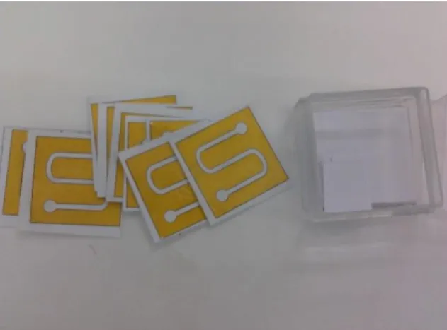
FIGURE 3.1–SNAKE SHAPED MASK CUT BY LASER. ... 9
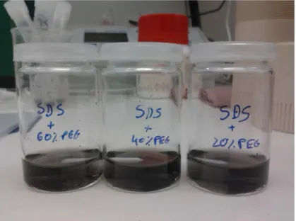
FIGURE 3.2–CNTS SOLUTIONS WITH VARIOUS CONCENTRATIONS OF PEG(60% V / V LEFT,40% V / V MID AND 20% V / V RIGHT). ... 10
FIGURE 3.3–SAMPLES AFTER DEPOSITION OF REUSED CNTS. ... 12
FIGURE 3.4–TWO DIFFERENT SAMPLES, ON THE LEFT SHOWING THE SOLUTION ACCUMULATION PROBLEM WITHIN THE RED CIRCLE AND ON THE RIGHT A SAMPLE WITH A UNIFORM FILM. ... 14
FIGURE 3.5–SEM IMAGES AT 5KV OF: A) AND B)NC3100NANOCYL CNTS; C) AND D)NC7000NANOCYL. ... 14
FIGURE 3.6-SOLUTION CONTACT ANGLE GRAPHICS IN FUNCTION OF TIME IN DIFFERENT TYPES OF PAPER: REGULAR PRINTING PAPER (A),FS2 PAPER (B),FS1 PAPER (C). ... 16
FIGURE 3.7–FS2 PAPER SURFACE SEM IMAGE (LEFT) AND THE RESPECTIVE PAPER SCHEME (RIGHT). ... 17
FIGURE 3.8–FS2 SAMPLES WITH SOLUTION 5 AND N=80(LEFT); SOLUTION 3 AND N=70(RIGHT). ... 17
FIGURE 3.9–TRANSISTORS WITH N=4, GOLD-NICKEL CONTACTS (YELLOW) AND WITH THE ELECTROLYTE DEPOSITED (BLACK BLOT OVER THE CONTACTS) COVERING CHANNEL, CONTACTS AND GATE. ... 19
FIGURE 3.10–SAMPLE WITH GOLD-NICKEL SOURCE, DRAIN AND GATE CONTACTS DEPOSITED IN FS2 PAPER. ... 19
FIGURE 3.11-TRANSISTOR (1,2) OUTPUT CURVE (LEFT) AND TRANSISTOR (3,2) OUTPUT CURVE (RIGHT). ... 20
xv
List of tables
TABLE 1–SAMPLES WITH REUSED CNTS. 12 TABLE 2–RESISTANCE VALUES FOR DEPOSITED CNT SOLUTIONS FROM MINHO. 13
General Introduction
1
1. General Introduction
1.1. Rise and attractiveness of carbon nanotubes (CNTs)
Carbon nanotubes had their origin in fullerene, discovered in 1985 by Richard Smalley and Harold Kroto [1]. This compound also known as the buckyball by its soccer ball shape has the chemi-cal formula C6o and consists in an allotropic form of carbon, the third more stable after the graphite and diamond. Methods were developed to obtain this compound, such as excimer laser pulse [2] or Kratschmer-Huffman carbon arc method [3, 4]. Moreover heterostructures fullerenes were made based in other elements than carbon, such as potassium [5], caged other materials inside them [6, 7] and, more recently, fullerenes were made using graphene, as shown in Figure 1.1.
Figure 1.1 - Experimental TEM images showing stages of fullerene formation directly from grapheme. [8]
A little later after this discovery, around 1991, carbon nanotubes were discovered by Sumio Li-jima that got them manufactured by a similar method that used to obtain fullerenes (C60), by arc-discharge evaporation [9]. S. Lijima demonstrated that it was possible to form these needle like struc-tures, composed by sheets of graphene, in which the carbon atoms are organized in hexagons, whose diameters ranged from a few, to some tens of nanometers.
Nowadays, CNT transistors are seen as a very attractive alternative for the replacement of con-ventional silicon transistors or even oxides, due to exceptional electrical, mechanical, and thermal properties that they present [10]. It has been reported carrier mobilities of about 10000 cm2×V-1×s-1 in individual SWCNT [11] that surpass the values usually observed in silicon. Moreover, thermal conduc-tivity at room temperature is around 3500 W.m-1.K-1 and the young modulus is 1TPa, matched only by graphene and surpassed by diamond, and tensile strength is 130 GPa) [12].
General Introduction
2
conventional metal-oxide-based sensors in terms of power consumption, sensitivity, miniaturization, and reliable mass production [19].
Figure 1.2 – Schematic of SWCNT e MWCNT (adapted from [20]).
What remains the main challenge is the ability to mass-produce CNTs and have a precise con-trollability over their physical properties (size, diameter, thickness, etc) and alignment of the arrays produced. Therefore it is necessary to further develop and optimize the parameters that are critical in the various methods of producing these thin films.
1.2. Thin film deposition methods for CNT solutions
Currently, flexible electronics is an area with great potential of development and, thus CNTs are a viable alternative to other semiconductors, and even to oxides and organics, combining its figure of merit, flexibility with high transparency (equivalent to ITO – Indium Tin Oxide – commercially using) [21]. Consequently different methods of deposit CNTs thin films from solutions have been developed, including dip coating [22], electrophoretic deposition [23] or filtration [24].
The printing techniques are very promising in this area due to its simplicity and high manufactur-ing yield. This means that vacuum and lithographic processes can be avoided, givmanufactur-ing a great possibility to replace the conventional semiconductor processing techniques by screen, gravure or inkjet printing. This way it is possible to avoid lithographic and providing a quick and low-cost alternative in the
manu-facture of flexible electronics based on carbon.
The inkjet printing technique (Figure 1.3) is relatively simple because makes used of equipments similar to our common "desktop" printers. However there are many details and parameters that must
General Introduction
3
instance it is quite tricky to keep SWCNT dispersed evenly in solution, as these tend to aggregate and form non-conductive mixtures [25].
Figure 1.3 – Schematic piezoelectric Inkjet Printing technique in the deposition of MWCNT. (adapted from [14])
P. Chen et al. reported the deposition of a thin film containing SWCNT with lengths being 0.5 to 1.5 µm, in a transparent polymeric substrate PET (poly(ethylene terephthalate)). A transmittance of 80% was achieved in the wavelength of visible light (400 – 700nm), to a thickness of 20 nm, and a sheet resistance of 78 Ω/sq to a thickness of 0.2 µm [26].
To deposit thin films, it is not only important the ink used and the treatment that is given to the ink itself, but all the process parameters such as the diameter of the nozzle and the speed with which the ink is extracted from it. Moreover substrate conditions, such as humidity and temperature, are also very important to assure a uniform and defect free thin film. J. Song et al. demonstrated that the dep-osition of SWCNT, by inkjet printing, on glass substrate heated at 60 ℃, makes the SWCNT network better organized, as the droplet dries almost instantly on contact with air. It was also concluded that it is desirable to make a surface treatment prior to the deposition in order to turn it more hydrophilic [27].
In addition to all applications covered by this versatile technique, it is still possible to print elec-trochromic layers of MWCNT. Small et al. made deposition of a MWCNT ink with a Polyaniline com-posite in a polymeric substrate, verifying that with increasing number of layers, from 1 to 3, the sheet resistance decreased (from 5 KΩ/sq to 1.15 KΩ/sq), as well as the transmittance (68% to 30%). Plati-num and gold electrodes were used and applying voltage between -0.2 V and 0.8 V, it was observed that the colour changed from yellow to green [28].
General Introduction
4
paper, which allowed him to have large capillary forces and a wide contact area, in which the CNTs were efficiently deposited after the solvent evaporation. Because of that, on the paper is not necessary to remove the surfactants because it doesn’t affect significantly the conductivity. The same wouldn’t happen with glass, plastic, metal or silicon wafers, for example. This excellent adherence of the film leads to a great film strength against damage [15].
The potential of this technique in the production of flexible devices have been widely explored, having been deposited solutions of quantum dots [29] and produced LEDs (light emitting light diodes) and CNT FETs, whose layers were all deposited by inkjet printing.
1.3. Carbon nanotubes thin film transistors
Nowadays the thin film transistors are of great importance in modern active matrix displays, among other devices, as the basis of its operation. These are composed of a semiconductor layer that works as a channel through which a current will be modulated by the dielectric layer that will induce charges in the semiconductor. Two electrodes are also deposited (source and drain) in contact with the semiconductor layer to extract these charges (Figure 1.4). These layers are all deposited on a substrate.
Figure 1.4 – Scheme of FET with channel semiconductor, insulator, source, drain, gate and substrate lay-ers [30].
There are many candidate materials for the semiconductor layer of the transistor, such as ox-ides, amorphous silicon (a-Si), low temperature polysilicon (LTPS) and organic materials. . They can be selected taking into account the transparency, flexibility and manufacturing process cost, stability
and large area uniformity. What happens with many of the oxides used in transistors is despite good mobility of carriers, they don’t have enough flexibility and some are expensive. The same happen for the a-Si, which in addition has low mobility and flexibility, and the LTPS, both processes require high temperatures, vacuum and special processing labs. On the other hand the organics, although they use low temperatures in the production process, present limited electrical performance and chemical sta-bility [12, 31]. The CNTs are then a candidate to consider as they show good characteristics for all the parameters described above.
Despite the good properties presented by semiconductor layers made based on CNTs, there are still many aspects to be taken into account and that can be improved and many doubts still exist in defining the best way to produce and deposit these thin films. These films have good electrical
General Introduction
5
well as the lack of uniformity, can drastically decrease the mobility of electrons, since this represents a major barrier for an electron transition between nanotubes. On the other hand, a low density will cause problems in capacitance per unit area, since the coverage of the dielectric by the CNTs is not com-plete and therefore the capacitance will decrease. Q. Cao et al. managed to produce a dense and aligned SWCNT film (Figure 1.5), about 500 CNTs/µm, by Langmuir-Schaefer method. The film was composed by 99% of SWCNT (semiconductor character) and was able to reach a good on/off ratio, 103, and mobility in the range of 25 cm2.V-1.s-1 [13]. The purity of the semiconductor film is another important parameter because it can result in the decrease the on / off ratio.
Figure 1.5 – Dense aligned nanotube array (adapted from [13]).
The dimensions of the semiconductor channel, width (W) and length (L), are also crucial for the behaviour of the transistor. In devices that have a channel length greater than the average length of the tubes, the percolation theory is applied, and electron transport (mobility) is limited by the junctions between several CNTs. For devices where the channel length is short, there will be many tubes direct-ly connecting the source to the drain, which can be considered as a conventional transistor, in which the mobility is limited by the effects of scattering as well as the by tube - electrode (2RC) contact re-sistance. Alongside this, some of these tubes can be MWCNT and making this bridge will critically de-grade the on / off ratio. What D. Sun et al. found was that with the increase of the channel length of a transistor (the CNT semiconductor layer was 10 µm in length), from 10 µm to 100 µm, the on / off ratio increased about 5 orders of magnitude, while the current decreased only 1, due to the increased re-sistance [32].
The deposition of the semiconductor layer of the FET can also be made by inkjet printing tech-nique, with all the advantages and disadvantages which have been mentioned above. Nevertheless F. Sajed et al. proved that it was possible to construct a transparent transistor with all layers printed, in which is possible to see a layer of uniform SWCNT through a SEM image. The FET had an on/off ratio of 100, a mobility of 2.3 cm2.V-1.s-1 and a threshold voltage of 2V [31].
General Introduction
6
was stretched, verifying that the resistance of the channel decreases, and a field effect mobility of 0.67 cm2.V-1.s-1 has been achieved, for a stretching ratio of 1.6 [33]. It has been verified that good uniformi-ty, density and alignment of the film, are important factors in the electrical performance of the transis-tor, as well as a good contact between the semiconductor layer and the source and drain electrodes, in order to decrease physical barrier felt by electrons.
1.4. Motivation
What is proposed in this work is the fabrication of an electrolyte gated transistor on paper, used as substrate, with MWCNT channel deposited based on printing techniques. An attempt was made to create the CNT ink as much dispersed as possible, with high CNT concentration, in order to create dense films to be printed by spray coating. A lot of spray tests were made to find the best parameters to achieve a film with good properties and low resistance, with the minimum number of layers. Inkjet printing was also tested, with some solutions, but it was a bit harder to fulfill the necessary parame-ters, such as viscosity, surface tension, CNT size, to make a printable solution.
Methods and Procedures
7
2. Methods and Procedures
2.1. CNT ink formulation
As stated in the chapter 1.2, the CNTs inks can be quite challenging to do since there are many aspects to be taken into account. However, spray coating was used as primary option since formula-tion of the ink is much simpler.
The methods used for preparing the solution were based on literature [34], wherein the constit-uents were found to be:
The basis of the solution is only distilled water;
Surfactants / thickening agent: SDS (Sodium Dodecyl Sulfate); Triton X-100; PEG 400 (polyethylene glycol); P123 (PEG - PPG (polypropylene glycol) – PEG)
Functional materials: CNT (NC7000 Nanocyl); CNT (NC3100 Nanocyl); Functionalized
CNTs
The CNTs were dispersed in a 0.3 wt% water solution of surfactant (generally 10 ml to 30 mg) which may be either SDS (98.5%, Aldrich) or Triton X-100 (Baker), weighted with the aid of a analyti-cal balance (OHAUS, PA214C), and then takes the solution to be stirred, until SDS or Triton are com-pletely dissolved. Then were added 0.03 wt% (3 mg) of CNTs to the solution and placed in an ultra-sonic bath (Bandelin, Sonorex) for 45 minutes and to ultraultra-sonication (Scansci) at 8 KHz, 4 minutes (2 minutes + 2 minutes to avoid the heating of the solution) to help disperse the CNTs in the solution, so they do not become agglomerated but dispersed homogeneously. Finally, the CNT solution goes to centrifuge at 4000 RPM for 90 minutes to sediment the agglomerates and, at the end, with a volumet-ric pipet carefully remove the supernatant to a flask. In the case of some agglomerates are still visible, the centrifugation step must be repeated. Later it was found that ultrasonication for 8 minutes (4 x 2 min) was more effective, since the solution tended to become more concentrated.
For the preparation of solutions that were later used in the printer, for inkjet printing, PEG 400 was added to the solution. PEG was added because according to Heister E. et al [32], it stabilizes the CNT dispersion, since it was a good way of tuning viscosity and get a suitable value for inkjet printing. In this work, solutions were tested at three different concentrations of PEG 400 (Aldrich) in water: 20%, 40% and 60% v / v, in which 2 ml were removed and mixed with 2 ml of the previously prepared CNTs (50/50 v/v). In addition to PEG, P123 was also tested. Moreover also MWCNT, dispersions pre-pared at Minho University [35], were tested for inkjet deposition.
The NC7000 CNTs have an average diameter, length and purity of 9.5 nm, 1.5 µm and 90 %,
respectively, and NC3100 have 9.5 nm, 1.5 µm and more than 95 % of purity. Functionalized CNTs were made using NC7000, so they have approximately the same physical properties but have been
Methods and Procedures
8
2.2. Spray and inkjet printing deposition
The deposition of CNT solutions was done either with spray coating or inkjet. The first consisted of a gun which base supports the injection of compressed air and the container is fitted on the side where the solution is placed for printing. The printing was done on paper substrates of several types, such as regular printing paper (Figure 2.1), Wattman paper and two papers with nanoporous coating. Printing takes into account various parameters such as the distance of the gun to substrate, the pres-sure of the compressed gas, the temperature at which the substrate is submitted, for how long the so-lution is deposited, the substrate drying time between depositions and the number of deposition by substrate. The equipment that has been used to spray coating is shown in Figure 2.2a.
Figure 2.1 – Pasted samples with kapton tape in order to improve the temperature uniformity.
On the other hand inkjet printing was done using a modified Canon PIXMA IP4850 desktop printer (Figure 2.2b) with a resolution of 9600×2400 dpi. The CNTs based ink was previously prepared, filter (0,45 µm) solution and then inserted in a container that has a capacity of 1 ml. The desired pat-terns were printed on the paper substrates (mentioned above) which were cut into a square shape and placed in the appropriate slots in the substrate carrier (green circle in Figure 2.2b). In this case, few parameters that have to do with the solution itself must be controlled quite well, such as the viscosity that should be around 1.5 cp, surface tension of 35 mN×m-1 and the size of the CNTs have to be at least 100 times smaller than nozzle diameter that is around 50 µm (must not exceed 500 nm in length), to not clog the printer head.
Figure 2.2 – a) Spray coating kit; b) Printer for inkjet printing.
Results and Discussion
9
3. Results and Discussion
3.1. Spray tests
During the thesis numerous depositions were made to test various options that were available. CNTs inks with different compositions, including different types of CNTs, and different deposition pa-rameters were used. Although the technique has a great variability (all the modifications made on the inks, the conditions used in deposition, the different components in the solution, etc) it was still used,
since the objective was to observe, in general, the best combination of parameters that would enable the deposition of homogenous films. The results obtained are summarized in the Appendix A and from now on samples will be named using their respective code.
To test what would be the best surfactant, several depositions were made on commercial print-ing papersubstrates, with Triton X and SDS as surfactants (the most commonly used), usprint-ing kapton
masks cut by LASER (UNIVERSAL Laser Systems) with a snake shape (Figure 3.1),
Figure 3.1 – Snake shaped mask cut by LASER.
After using the multimeter to estimate the resistance, it was found that samples which were de-posited with Triton X-100 (A1) presented too high resistance values to be measured. On the other hand the films deposited from solution with SDS (A2) had measurable values on the multimeter,
be-tween 50 to 19 MΩ (Appendix A). Despite Triton X allow good dispersion, it was found that was not suitable for intended application, somehow preventing contact between the nanotubes, because re-sistances were too high (more than 200 MΩ).
Results and Discussion
10
Figure 3.2 – CNTs solutions with various concentrations of PEG (60 % v / v left, 40 % v / v mid and 20 % v / v right).
In a first approach it was concluded that be best results in terms of films' uniformity were ob-tained using only SDS. Based on this some more samples were prepared with SDS + 20% PEG (since in these samples multimeter was able to measure resistance values, although quite high), and some with only SDS.
In the following depositions the snake pattern has been abandoned, due to be quite complex at an early stage, where the main goal was to compare the different kinds of samples in terms of electri-cal resistance. Furthermore, this pattern had very thin lines, which were easily broken by removing the Kapton mask, and thus CNTs conducting channel could be interrupted
Subsequent SDS + 20% PEG deposition generated positive results, even with some result vari-ation due to the technique itself. In the sample A5 it was possible to reduce somewhat the amount of the resistance to 30 MΩ with n = 15 (n is the number of layers deposited). For the A6 substrates the deposition time was decreased to 1 seconds, because 3 seconds was too long and the samples were getting soaked. Thus, samples drying time was also decreased for 3 minutes between each deposition and 10 minutes after every 5 depositions.
In the next deposition batch (A7), the distance between the gun and substrates was greatly in-creased from 3 to 20 cm in order to get a better uniformity by improving the distribution of the jet on the samples and also pressure was increased to give a little compensation to the bigger separation of the gun to the substrate. For some reason this approach did not work and samples showed high re-sistance, unable to be measured by the multimeter (probably gun’s height was too high), even with n
= 10 in each substrate. Samples A8 were tested under the same conditions, but this time using SDS. The results were positive, but the resistance values remained very high, in the range of 10 - 20 MΩ.
Results and Discussion
11
drying under low vacuum and 50 ℃ and before washing, the resistance values are shown in Appendix A table. After washing the following results were obtained:
Sample A: Washed in water Showed infinite resistance Sample B: Washed in Ethanol Showed infinite resistance Sample C: Washed in IPA Showed infinite resistance Sample D: Was not washed Same resistance
The washing process seemed to remove a good amount of CNTs and thus prevented the inter-connection of the CNTs path.
A sample was tested without any mask (A9), that is, the solution was deposited directly on the paper heated at 100 °C without a pattern, to not interfere in any way in the process. Deposition time was then increased slightly and drying time was decreased in order to avoid the risk of burning the paper, since the substrates would be over heated and therefore would dry quickly. Gun’s height was also decreased to 10 cm due to worst results obtained with 20 cm. The result was a measurable amount of resistance and so the work continued in this direction, but using NC3100 Nanocyl in order to test another type of CNTs, analyze the results and compare them with the previous ones.
After all these trials, two more changes were made: the ultrasound treatment time was in-creased from 4 to 8 minutes, which proved to be a good modification because the solutions appeared to be more concentrated, although the CNTs used were different. To be sure this modification was good, the CNTs NC7000 Nanocyl samples, A14 and A15, were tested with the increase of ultrasound and the results were improved when compared with the samples A8 or A9, even with higher n in A8. The other modification consisted in gluing the samples (with sprayed glue) to the aluminium foil, in-stead of using Kapton tape. Kapton gives the paper rise to "crinkle" and solution tended to accumulate in some places after deposition. As a result, samples were obtained with a better uniformity across the exposed area that can result also from a better temperature uniformity on the substrates.
Samples A10 and A11 depositions were performed on Wattman and regular printing paper, wherein Wattman paper seems to be a bit worse in terms of resistance results, since its high porosity makes it inappropriate (as will be seen later in Chapter 3.2). This particular characteristic of Wattman paper is bad for the objectives of this work, because for the deposition of semiconductor channel, it is needed a mask of kapton with the right pattern and this high porosity mean that solution will not be restrained in the pattern region. Thus, in this case, high porosity means a higher weakness, and a ro-bust paper is important when the kapton tape is removed, otherwise paper is pulled.
Results and Discussion
12
Initially, it was already expected that the reuse of CNTs was not something that would be worth, unless many depositions were made, because the whole process has to be made again. All the steps and in particular the dispersion of CNTs in solution through ultrasonication, will create defects on them and therefore they will become more resistive [38]. Moreover, after CNTs clusters are collected and reused, the amount will be obviously smaller, which may also influence.
Figure 3.3 – Samples after deposition of reused CNTs.
Finally, NC7000 CNTs were used again due to small amount of NC3100 available. In A16 sam-ple, NC7000 CNTs have been subjected to a process of carboxylation where carboxyl groups are at-tached to the sidewalls of CNTs via various chemical reactions with acids. These reactions create de-fects on CNTs, but can be compensated by an enhancement on their dispersion, thus the resistance values were similar to NC3100.
It was concluded from these tests that the best deposition conditions are a pressure of 4 bar, distance of 10 cm, 3 seconds of deposition on regular printing paper substrates and 90 seconds of drying time between depositions and heating the substrates at 100 °C. The best results in terms of resistance were obtained with NC3100 CNTs, however a resistance value in range of few MΩ was needed and then NC7000 were used to make the transistor semiconductor channel.
Still, further tests were performed, reutilizing CNTs with ideal conditions, as shown previously, in which a standard solution with NC7000 was made, and deposited on 8 paper substrates at once. At the end, the remaining CNTs after centrifugation were reused and a new solution was made, that was deposited only on seven substrates, which had been previously used, and so on until only one sub-strate remained for all the depositions. The results obtained for reused CNT are presented in Table 1:
Table 1 – Samples with reused CNTs.
Samples B1 B2 B3 B4 B5 B6 B7 B8
n 5 13 (+8) 19 (+6) 24 (+5) 31 (+7) 36 (+5) 43 (+7) 50 (+7)
Resistance
Results and Discussion
13
Given this scenario, It can be seen that it is possible to reach very low resistance values, as 6kΩ, but it took an n = 50. Probably if the best CNTs had been used, n would not need to be so high.
B8 sample was measured by Hall Effect. For this, the paper was cut up into a square and silver glue placed in each vertex to serve as a contact. The necessary parameters have been adjusted and the results are shown below:
Majority carriers - p - type; Sheet resistivity - 1,53 × 10³ Ω/□ Hall mobility - 0,206 cm2/V.s
Sheet carrier concentration - +1,98 × 1016 cm-2
CNTs normally have ambipolar behaviour, in other words, they have the ability to conduct both electrons and holes, however at ambient temperature hole transport predominate [10], as shown by the results. Both carrier concentration and resistivity, values are within the range of normal values for a semiconductor material, compared for example with a semiconducting amorphous oxide [39].
After all these tests, other solutions that came from Minho University have been tried: MWCNT dispersions with appropriate CNTs size and viscosity (lenght less than 500 nm and viscosity of 1.5 cp) also for inkjet printing. These solutions were dispersed in a buffered aqueous solution of bolaam-phiphilic perylene bisimides (organic molecules) [35], a different approach from what have been done for dispersing CNTs in this thesis. These were deposited on FS2 (a nanoporous paper designed to be used for inkjet printing) paper with the same deposition conditions and resistance values are listed in Table 2:
Table 2 – Resistance values for deposited CNT solutions from Minho.
n = 1 n = 4 n = 6 n = 8
Solution 3 N/A N/A 3 MΩ 700 KΩ
Solution 4 N/A 15 MΩ 1.4 MΩ 140 KΩ
Solution 5 N/A 1.5 MΩ 60 KΩ 100 KΩ
Solution 8 N/A 210 KΩ 120 KΩ 45 KΩ
Solution 9 N/A 160 KΩ 50 KΩ 20 KΩ
Solution 10 10 MΩ 200 KΩ 70 KΩ 30 KΩ
The difference between solutions 3, 4 and 5 are the CNTs concentration, they have 0,05 mg/mL, 0,075 mg/mL and 0,1 mg/mL, respectively, and PH 7. The other three solutions have exactly the same CNT concentration, by the same order, but PH is 11. By observing Table 2, it is clear that the bottom half of the table has slightly better results. In fact, just by observation, solutions 8 – 10 were darker, which mean that were more concentrated too.
Results and Discussion
14
giving less time to the solution to accumulate in certain regions. As previously stated, uniformity is a crucial parameter with regard to CNTs films, so it was considered in the various tests which have been carried out. In Figure 3.4 an example of the differences between two samples can be seen: at the left a sample with a non-uniform film with kapton mask, attached with kapton tape and deposited at 25 ºC and at right a sample with a good film uniformity after optimization.
Figure 3.4 – Two different samples, on the left showing the solution accumulation problem within the red circle and on the right a sample with a uniform film.
Also some nanotube images were taken to observe how the CNTs look like (Figure 3.5), through a SEM equipped with a Schottky Field Emitter, resolution of 1.0 nm - 15 kV, 1.9 nm - 1 kV and acceleration voltage between 0.1 and 30 kV.
Figure 3.5 – SEM images at 5 KV of: a) and b) NC3100 Nanocyl CNTs; c) and d) NC7000 Nanocyl.
a) c)
Results and Discussion
15
3.2. Inkjet printing tests
At the same time of deposition tests were made by spray coating, some tests for inkjet printing were also carried out, since the original idea was to print a whole transistor using this technique. (Chapter 2.2).
What was attempted to do was a solution with an organic solvent dimethylformamide (DMF), because a few studies suggest this compound would be good to do solutions whose purpose would be inkjet printing [24, 33]. However in both references SWCNT were used. Accordingly, it has been found that with 10 mL of DMF and 1 mg of CNTs solution was not highly concentrated in terms of CNTs, many agglomerates remained, even after centrifugation. This happened probably because MWCNT have been used and DMF is more suitable for SWCNT.
Firstly, the standard SDS solution that had been employed in the spray coating deposition, has too low viscosity for use in inkjet printing. Density of water (reference liquid) and SDS solution were measured 10 times in a homemade capillary viscometer, in order to get a good estimate. Equation 1 was used to calculate viscosity:
𝜼
𝒙= 𝜼
𝒓𝒆𝒇𝝆𝒓𝒆𝒇𝝆𝒙.𝒕.𝒕𝒙𝒓𝒆𝒇 Equation 1wherein 𝜂𝑥 and 𝜂𝑟𝑒𝑓 represent the viscosity of the liquid to be measured and the reference (water), respectively, 𝜌 is the density and 𝑡 the time that the liquid takes to move from one point to another of the pipette. The viscosity of water at 24 ºC (room temperature in which the measurements were made) was seen in the literature, 0.894 cp, and the respective densities were calculated by dividing the mass by the volume. The viscosity measurement results were as follows:
SDS = 0,704 cp
SDS + Ethanol = 1,543 cp
SDS + Ethylene Glycol (ETG) = 2,303 cp
The solution with the ideal viscosity would be SDS with ethanol, but ethanol and ETG do not disperse CNTs and therefore these components along with the SDS also does not effectively disperse them. The PEG solution was then used in order to print CNTs, even though viscosity couldn’t be measured by the method described above because the solution was non-Newtonian; it contains a pol-ymeric compound. The NC 7000 CNTs have 1.5 µm length so PEG solutions were filtered with a 0.45 µm in order to not clog the printer nozzle. After performing some printing tests, two situations were quickly found: that regular printing paper was not the most appropriate, because its too high hydro-philicity meaning that, after several depositions (even with drying time between depositions around 12 s [24] at room temperature), the patterns would not be well defined. Furthermore CNTs concentration was too low or the parameters of viscosity or surface tension of the solution were not correct, because it was necessary a large n to begin to notice that something was deposited on the substrate, usually n
Results and Discussion
16
µm, and only the ones that were damaged and broken or those who are perfectly aligned with the filter pores would pass through it.
Given the circumstances, 4 different papers were tested (which are mentioned above in section 2.2): regular printing paper, wattman paper and 2 special inkjet paper substrates with different coat-ings (FS1 and FS2). Contact angle of the SDS solution + 20% PEG without CNTs was measured in Contact Angle System OCA (Dataphysics).
Figure 3.6b) graph is the one that shows a more regular behavior in terms of contact angle over time. In the regular printing paper (graph a)) the contact angle is shown to be higher than paper FS2 in the first seconds, but it is observed that the paper is quickly wetted by the solution drop in 4 seconds, the angle decreases from 45º to 10º. Thus, it is apparent that the solution in this paper spreads very easily, hence the difficulty in maintaining well-defined patterns. In contrast, the FS1 paper (graph c)) was too hydrophobic, so after some depositions it was noticed that several droplets of solution did not dry out. These arguments suggest FS2 as the best alternative, because the angle lowers smoothly and stabilizes in a suitable value for a slowly drying of droplets, without wetting paper too much. The Wattman paper graph is not shown because the drop seeps instantly within the paper porosities, pret-ty much the same logic that underlies the explanation of previous chapter. In the following depositions FS2 was used, that is a commercial Felix Schoeller ® paper based substrate with hydrophilic nanopo-rous surface, with 205 µm thickness, mostly with pore size lower than 100 nm (Figure 3.7)
Figure 3.6 - Solution contact angle graphics in function of time in different types of paper: regular print-ing paper (a), FS2 paper (b), FS1 paper (c).
Results and Discussion
17
Figure 3.7 – FS2 paper surface SEM image (left) and the respective paper scheme (right).
After finding the most suitable paper substrates, solutions from U. Minho were tested once again, but now with inkjet printing. These inks were deposited in two samples shown in Figure 3.8, in which the left sample has n = 80 and the right sample has n = 70, with solution 5 and 3, with CNT concentration of 0.1 mg/mL and 0.025 mg/mL, respectively. The samples after deposition showed re-sistance values of MΩ, but when left to dry from one day to the other, resistances were too high and multimeter no longer measured anything. Considering this, it can be inferred that the solution some-how made the CNTs to be interconnected and when it evaporates, the CNTs dispersed on paper do not form a conductive path.
Figure 3.8 – FS2 samples with solution 5 and n = 80 (left); solution 3 and n = 70 (right).
The surface tension of these two solutions was measured using a stalagmometer to count the drops of the solutions within a certain time. The surface tension is given by Equation 2:
Results and Discussion
18
where 𝜎𝑟𝑒𝑓 is the relative surface tension, 𝜎𝑥 is the surface tension of the CNTs solution, 𝜎𝑟𝑒𝑓 is the surface tension of the reference liquid (in this case water), 𝑛 is the number of drops and 𝜌 is the density of liquid. After the measurements of distilled water and both solutions, the results were 𝑛𝑟𝑒𝑓= 19 and 𝑛𝑥= 19 and density for both, water and CNT solution, were approximately 1, because solu-tions were water based. Since 𝜎𝑟𝑒𝑙= 1, means that surface tension of the solutions is the same as water, and 𝜎𝑟𝑒𝑓 = 𝜎𝑤𝑎𝑡𝑒𝑟 at room temperature is 75 mN×m-1. At this surface tension the meniscus at the nozzle is too high which prevents the droplet generation. Because of that, the amount of printed liquids is too small as the generated droplets are very small.
This surface tension value does not match the ideal value of 35
mN×m
-1, which is stated in chapter 2.2. In consequence this may cause the ink to not wet out the substrate effectively, resulting in uneven prints.3.3. Carbon Nanotubes transistor
In order to make the CNT transistors it was used the information that has been collected previ-ously, ie, the best conditions for the deposition of solutions, whose results are presented in chapter 3.1, and the best type of paper, that is FS2. With the help of optical microscope (OLYMPUS, BX51), length and width of metallic masks, usually used for semiconductor deposition, were measured (Appendix B, Appendix C and Appendix D), so those mask can be reproduced exactly with the same size but in kapton, cut by laser. Then, kapton masks were putted on FS2 paper and the NC 7000 CNTs solution was sprayed. 3 samples, one with n = 1 and two with n = 2 depositions, were made and then gold-nickel contacts were deposited above semiconductor channel, in a controlled clean room environment. Results obtained were not good because channel must be over the contacts to avoid having a large proportion of the electrolyte making direct connection with the source and drain con-tacts, since this can enhance leakage currents and damage the transistor. Staggered configuration is always preferred in this case.
Results and Discussion
19
Figure 3.9 – Transistors with n=4, gold-nickel contacts (yellow) and with the electrolyte deposited (black
blot over the contacts) covering channel, contacts and gate.
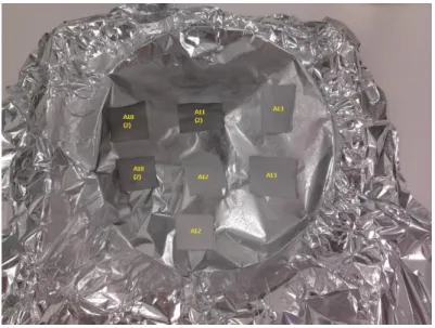
The transistors were tested in Semiconductor Characterization System (Keithley 4200-SCS) with a Cryogenic Equipment by JANIS Probe Station. It is also equipped with an Illumination and Mi-croscope system by Edmund Optics Worldwide MI-150 HIGH-INTENSITY ILLUMINATOR for image acquisition. It was concluded that the devices in the center of the substrates were the ones performing better. The channel was about 1 x 0.2 mm (Figure 3.10). If we consider a plan with xy coordinates, in which the larger transistors are at the coordinates (1, 1) and (3, 3) and smaller at the coordinates (1, 3) and (3, 1), it is evident that they are not in a central position (Figure 3.10). It is therefore more likely that the deposition of the CNTs does not reach so effectively that zone, creating a less dense and ho-mogeneous film, thus compromising performance, or leading transistors do not work at all. Additional-ly, the smaller sizes of the shorter transistors mean that it is quite complicated to manually align the mask with the contacts. Accordingly, the transistors that worked better had coordinates (1, 2) and (3, 2) in the samples with n =4.
Figure 3.10 – Sample with gold-nickel source, drain and gate contacts deposited in FS2 paper.
200 µm 200 µm
Results and Discussion
20
The analysis of the transistors was made using OriginLab 8, wherein their transfer and output curves were done and where all the relevant values in the characterization of a transistor were calcu-lated. As already known from Chapter 3.1, CNTs are p-type and the graphs shown in Figure 3.11 are quite similar characteristic output curves of p-type electrolyte gated transistors, with 𝑉𝑑= −0.5 𝑉. Transistor (1, 2) has slightly higher currents, around 70 μA (microamperes), while the (3, 2) has a maximum current of 33 μA for the same gate voltage value, -4 V.
This electrolyte in particular has a capacitance of 5,1 × 10⁻⁶𝐹. 𝑐𝑚−2, a typical value for this type of material [40]. Moreover it was also found a non-saturation behavior in both graphics, something that can commonly occur in transistors by short channel effect, which clearly is not the case here (L is 0.2 mm), or due to a low Vds voltage applied because polymeric electrolytes cannot endure large voltages.
Figure 3.11 - Transistor (1, 2) output curve (left) and transistor (3, 2) output curve (right).
In the following transfer curves (Figure 3.12) of both transistors, with 𝑉𝐷= −0.5 𝑉, significant dif-ferences can be noted in the shape of the curve. It is observed that the transistor (1,2) current begins to increase for positive voltages, which is not a called ideal behavior, which means that at 0 V the transistor channel is substantially open (deplection mode). Maximum current is hundreds of µA, 𝑉𝑂𝑁 cannot be clearly extrapolated in the graph and the On/Off ratio is given by:
𝑶𝒏/𝑶𝒇𝒇 𝒓𝒂𝒕𝒊𝒐 =
𝑰𝑫𝒎á𝒙𝑰𝑫𝒎í𝒏 Equation 3
Results and Discussion
21
Figure 3.12 - Transistor (1, 2) transfer curve and transistor (3, 2) transfer curve.
In the graph on the right of Figure 3.12 is shown the transfer curve of the transistor (3, 2) which is similar to the previous one, but is "shifted" a little to the left on the x axis, so the 𝑉𝑂𝑁 lies around 0.5 V, which represents a more ideal value. The maximum current is located in the tens of µA and on/off ratio keeps having very low values, in this case even slightly lower than the previous.
(𝟑, 𝟐) 𝑶𝒏/𝑶𝒇𝒇 𝒓𝒂𝒕𝒊𝒐 =𝟐. 𝟏𝟏 × 𝟏𝟎𝟑. 𝟑 × 𝟏𝟎−𝟓−𝟓≈ 𝟏. 𝟓
Leakage currents are lower for transistor (3, 2), about 10-7, but both values are acceptable. The rest of the parameters were calculated based on the appendix graphs, from Appendix F to Appendix K. VT was calculated based on Appendix F and Appendix I, in which by a linear interpolation of straight of Figure 3.12 graphs (for low Vds), it is obtained the straight-line equation and the point of interception with the xx axis is easily calculated, which gives VT value. Therefore it follows that:
(𝟏, 𝟐) 𝑽𝑻=−𝟏. 𝟐𝟑𝟕 × 𝟏𝟎
−𝟒
−𝟏. 𝟐𝟗𝟏 × 𝟏𝟎−𝟓= 𝟗. 𝟔 𝑽
(𝟑, 𝟐) 𝑽𝑻=−𝟐. 𝟏𝟗𝟏 × 𝟏𝟎
−𝟓
−𝟑. 𝟐𝟓𝟎 × 𝟏𝟎−𝟔= 𝟔, 𝟕 𝑽
The Subthreshold swing (SS) was calculated from the graphs of Appendix G and Appendix J, given by the following equation:
𝑺 = (
𝝏𝐥𝐨𝐠 (𝑰𝑫)𝝏𝑽𝒈
|
𝒎𝒂𝒙)
−𝟏
Equation 4
SS is calculated by the inverse of the peak in both graphs:
Results and Discussion
22
(3,2) 𝑆𝑆 =0.0546 = 18.3 V/dec1
Finally, the field effect mobility was calculated from the equation:
𝝁
𝑭𝑬=
𝑪𝒈𝒎𝒊𝑾𝑳𝑽𝑫
Equation 5
Since the W (width) is approximately 1 mm and L (length) is 0.2 mm, it can be considered that the W / L of the transistor is 5 (Appendix E). As mentioned, Vds = -0,5 V, an estimated gate Ci (electro-lyte capacitance) of 5,1 × 10⁻⁶𝐹. 𝑐𝑚−2 and gm (transconductance) is seen by the minimum point of the graphs of Appendix H and Appendix K.
(1,2) 𝑔𝑚= −1.36 × 10⁻⁵𝑆 ⇒ 𝜇𝐹𝐸 = −1.36 × 10
−5
5,1 × 10−6× 5 × (−0,5) = 1.07
𝑐𝑚2
𝑉. 𝑠
(3,2) 𝑔𝑚= −3.49 × 10⁻⁶𝑆 ⇒ 𝜇𝐹𝐸= −3.25 × 10
−6
5,1 × 10−6× 5 × (−0,5) = 0.254
𝑐𝑚2
𝑉. 𝑠
Table 3 – Parameters summary of both transistors.
Transistor (1, 2) (3,2)
On/Off ratio 1.8 1.5
𝑽𝑶𝑵 [v] 3.7 0.5
Max Leakage Current [A] 1 × 10⁻⁷ 4 × 10⁻⁶
𝑽𝑻 [V] 9.6 6.7
Subthreshold Swing [V/dec] 16.3 18.3
𝝁𝑭𝑬 [𝒄𝒎
𝟐
𝑽. 𝒔 ] 1.07 0.254
In the first analysis it is noted that despite both transistors being part of the same substrate, meaning that were made in exactly the same conditions, these still have quite different values with respect to VON, VT, or even field effect mobility (Table 3).
Results and Discussion
23
have achieved field-effect mobility of 1.07 cm2/V×s, what is an acceptable value for an electrolyte gat-ed transistor.
Maximum currents are tens and hundreds of μA that are good values for a transistor, which may indicate a relatively dense film, where there is a network of interconnected MWCNT. The denser the network is, the lower the resistance of the semiconductor as there are more points of contact between the several CNTs, and more charges can be induced by the electrolyte gate, as explained in the intro-ductory chapter. This technique does not allow any kind of CNT arrangement, so the alignment of these have no preferred direction. It can also take into account the parasitic resistances created by existing schottky barriers between the metal contacts and the channel, increasing the total resistance (RT), which if it is too high can have great influence on the maximum current flowing through the tran-sistor, and the CNT - CNT resistance that can have high influence because channel length is much greater (100x) than CNT length. Oxidation of metal contacts and traps that can be created between the dielectric and the channel, where carriers can be trapped, are also main concerns.
Conclusion
24
4. Conclusion
All the matter involving this theme, which although very interesting, is also very challenging, is relatively new in the Materials Research Center (CENIMAT). Thus, the evolution of this work, with view of creating electrolyte gated transistors with printed MWCNTs channel as the final result, was gradually made by well-defined but also very small steps. All work was developed based on previous studies by CENIMAT researchers, the existing literature on the subject or sometimes by trying to do something new.
Initially, the first tests in the dispersion of MWCNTs were performed, where, in a very general way, the reactants that are best suited to a homogeneous dispersion of CNTs were analyzed, whose concentration is wanted to be the highest possible. It was concluded that most effective way to dis-perse the CNTs, at all levels, was only with SDS within the tested dispersants.
It was always kept in mind throughout the whole work that besides being necessary to create a solution more uniform and concentrated as possible, it would be also a priority to keep the dispersion method simple because the amount of tests that would be required to do, with a huge amount of vari-ables, demanded that the solution did not take much time to be done. The standard solution that was used throughout the work, water and CNTs with SDS, at best took an average of 200 minutes to be made, so always remained a little distant the idea of involving functionalization processes of CNTs (which is largely made on existing bibliography) or any other time-consuming reactions. However in future work the use of acid functionalized or better CNTs (the case of NC 3100) should be taken into account, because as it turned out they provide better outcomes in terms of resistance, comparatively to the non-functionalized.
After numerous tests with various depositions made by spray coating varying the several pa-rameters, by observation of the deposited films and through the help of the multimeter to get an idea of the resistance’s magnitude of these, it was found 100 ° C, 4 bar, 10 cm height, 5 seconds of deposi-tion time and drying time of 90 seconds between steps to be the best deposideposi-tion parameters. These were then being used in the rest of the thesis, including the deposition of the semiconductor layer of the transistor. More tests can be done, diversifying the parameters and with different solutions, in the direction of improving the obtained results.
Conclusion
25
However this would have a negative impact in large length channels since more contact point are re-quested to achieve a continuous path for electrons between source and drain
In the final stretch of the thesis the desired objectives were achieved, managing to modulate the current of a transistor made with MWCNT. The results were based on the previous studies, about how to optimize deposition conditions, and because of this, reasonable results were yielded with regard to the characterization of the transistor itself. Although the On / Off ratio is not very high, a low leakage current was evidenced by both transistors and mobility of 1.07 cm2/V×s in one of them.
Regardless of the results are adequate for this type of transistors (electrolyte gated) some of the properties of the MWCNTs film were not optimized, such as the thickness. It would be very important to be able to control in detail the thickness of the semiconductor layer, because only the channel sur-face in contact with the electrolyte is affected by the electrolyte induced charges. So, a good controlla-bility over the film is essential to test several thicknesses and analyze how the transistor reacts. An-other important modification would be the use of SWCNTs, which is known to have semiconducting character, a crucial property for the improvement of On / Off ratio and all other parameters of transis-tor. An interesting thing to be done, was the CNTs characterization under mechanical stress, stretch-ing and bendstretch-ing, since the substrate in question was malleable.
It should also be possible to improve transistor performance using a more adequate electrolyte. Despite the fact this electrolyte has a good capacitance, it was a cationic electrolyte that is not totally appropriate for hole conducting semiconductors.
Bibliography
26
5. Bibliography
1
H.W. Kroto, J.R. Heath, S.C. Obrien, R.F. Curl and R.E. Smalley, Nature 318,
162-163 (1985) doi: 10.1038/318162a0
2
Y. Liu, S.C. Obrien, Q. Zhang, J.R. Heath, F.K. Tittel, R.F. Curl, H.W. Kroto
and R.E. Smalley, Chemical Physics Letters 126, 215-217 (1986) doi:
10.1016/s0009-2614(86)80042-2
3
R.E. Haufler, J. Conceicao, L.P.F. Chibante, Y. Chai, N.E. Byrne, S. Flanagan,
M.M. Haley, S.C. Obrien, C. Pan, Z. Xiao, W.E. Billups, M.A. Ciufolini, R.H. Hauge,
J.L. Margrave, L.J. Wilson, R.F. Curl and R.E. Smalley, Journal of Physical Chemistry
94, 8634-8636 (1990) doi: 10.1021/j100387a005
4
D.S. Bethune, C.H. Klang, M.S.d. Vries, G. Gorman, R. Savoy, J. Vazquez and
R. Beyers, 363, 605-607 (1993) doi: doi:10.1038/363605a0
5
D.M. Poirier, T.R. Ohno, G.H. Kroll, Y. Chen, P.J. Benning, J.H. Weaver, L.P.F.
Chibante
and
R.E.
Smalley,
Science
253,
646-648
(1991)
doi:
10.1126/science.253.5020.646
6
Y. Chai, T. Guo, C.M. Jin, R.E. Haufler, L.P.F. Chibante, J. Fure, L.H. Wang,
J.M. Alford and R.E. Smalley, Journal of Physical Chemistry 95, 7564-7568 (1991) doi:
10.1021/j100173a002
7
D.S. Bethune, R.D. Johnson, J.R. Salem, M.S.d. Vries and C.S. Yannoni, 366,
123-128 (1993) doi: doi:10.1038/366123a0
8
A. Chuvilin, U. Kaiser, E. Bichoutskaia, N.A. Besley and A.N. Khlobystov,
Nature Chemistry 2, 450-453 (2010) doi: doi:10.1038/nchem.644
9
S. Iijima, Nature 354, 56-58 (1991) doi: 10.1038/354056a0
10
S. Yun, S.-D. Jang, G.-Y. Yun, J.-H. Kim and J. Kim, Applied Physics Letters 95,
104102-104102-104103 (2009)
11
X. Ho, L. Ye, S.V. Rotkin, Q. Cao, S. Unarunotai, S. Salamat, M.A. Alam and
J.A. Rogers, Nano letters 10, 499-503 (2010)
12
D.M. Sun, C. Liu, W.C. Ren and H.M. Cheng, Small, (2013)
13
Q. Cao, S.J. Han, G.S. Tulevski, Y. Zhu, D.D. Lu and W. Haensch, Nature
Nanotechnology 8, 180-186 (2013) doi: 10.1038/nnano.2012.257
14
O.S. Kwon, H. Kim, H. Ko, J. Lee, B. Lee, C.H. Jung, J.H. Choi and K. Shin,
Carbon 58, 116-127 (2013) doi: 10.1016/j.carbon.2013.02.039
15
L.B. Hu, J.W. Choi, Y. Yang, S. Jeong, F. La Mantia, L.F. Cui and Y. Cui,
Proceedings of the National Academy of Sciences of the United States of America
106, 21490-21494 (2009) doi: 10.1073/pnas.0908858106
16
H. Shimoda, B. Gao, X.P. Tang, A. Kleinhammes, L. Fleming, Y. Wu and O.
Zhou, Physical Review Letters 88, 4 (2002) doi: 10.1103/PhysRevLett.88.015502
17
C. Niu, E.K. Sichel, R. Hoch, D. Moy and H. Tennent, Applied Physics Letters
70, 1480-1482 (1997)
18
K.H. An, W.S. Kim, Y.S. Park, J.M. Moon, D.J. Bae, S.C. Lim, Y.S. Lee and Y.H.
Lee, Advanced functional materials 11, 387-392 (2001)
19
P. Qi, O. Vermesh, M. Grecu, A. Javey, Q. Wang, H. Dai, S. Peng and K. Cho,
Bibliography
27
20
M.C.
Hersam,
Nature
Nanotechnology
3,
387-394
(2008)
doi:
doi:10.1038/nnano.2008.135
21
M. Endo, M.S. Strano and P.M. Ajayan, Carbon Nanotubes 111, 13-61 (2008)
22
M. Jung de Andrade, M. Dias Lima, V. Skákalová, C. Pérez Bergmann and S.
Roth, physica status solidi (RRL)-Rapid Research Letters 1, 178-180 (2007)
23
S. Pei, J. Du, Y. Zeng, C. Liu and H.-M. Cheng, Nanotechnology 20, 235707
(2009)
24
M. Zhang, S. Fang, A.A. Zakhidov, S.B. Lee, A.E. Aliev, C.D. Williams, K.R.
Atkinson and R.H. Baughman, Science 309, 1215-1219 (2005)
25
M. Singh, H.M. Haverinen, P. Dhagat and G.E. Jabbour, Advanced Materials
22, 673-685 (2010) doi: 10.1002/adma.200901141
26
P.C. Chen, H.T. Chen, J. Qiu and C.W. Zhou, Nano Research 3, 594-603 (2010)
doi: 10.1007/s12274-010-0020-x
27
J.W. Song, J. Kim, Y.H. Yoon, B.S. Choi, J.H. Kim and C.S. Han,
Nanotechnology 19, 6 (2008) doi: 10.1088/0957-4484/19/9/095702
28
W.R. Small, F. Masdarolomoor and G.G. Wallace, Journal of Materials
Chemistry 17, 4359-4361 (2007)
29
H.M. Haverinen, R.A. Myllyla and G.E. Jabbour, Applied Physics Letters 94,
073108-073108-073103 (2009)
30
M.E. Roberts, A.N. Sokolov and Z. Bao, (2009) doi: 10.1039/B816386C
31
F. Sajed and C. Rutherglen, Applied Physics Letters 103, 4 (2013) doi:
10.1063/1.4824475
32
D.-m. Sun, M.Y. Timmermans, Y. Tian, A.G. Nasibulin, E.I. Kauppinen, S.
Kishimoto, T. Mizutani and Y. Ohno, Nature nanotechnology 6, 156-161 (2011)
33
J.H. Kim, S. Yun, H.U. Ko and J. Kim, Current Applied Physics 13, 897-901
(2013) doi: 10.1016/j.cap.2013.01.036
34
A. Schindler, S. Spiessberger, N. Fruehauf, J.P. Novak, Z. Yaniv and P. East
China Normal Unviersity, AD'07: Proceedings of Asia Display 2007, Vols 1 and 2,
882-887 (2007)
35
R.F. Araujo, C.J.R. Silva, M.C. Paiva, M.M. Franco and M.F. Proenca, Rsc
Advances 3, 24535-24542 (2013) doi: 10.1039/c3ra42422g
36
S. Sattari, A. Reyhani, M.R. Khanlari, M. Khabazian and H. Heydari, Journal
of
Industrial
and
Engineering
Chemistry
20,
1761-1764
(2014)
doi:
10.1016/j.jiec.2013.08.029
37
Y. Gendel, H. Roth, A. Rommerskirchen, O. David and M. Wessling,
Electrochemistry Communications 46, 44-47 (2014) doi: 10.1016/j.elecom.2014.06.006
38
R.P. Tortorich and J.-W. Choi, Nanomaterials 3, 453-468 (2013)
39
A. Takagi, K. Nomura, H. Ohta, H. Yanagi, T. Kamiya, M. Hirano and H.
Hosono, Thin Solid Films 486, 38-41 (2005) doi: 10.1016/j.tsf.2004.11.223
40
S.H. Kim, K. Hong, W. Xie, K.H. Lee, S. Zhang, T.P. Lodge and C.D. Frisbie,
Appendices
28
6. Appendices
Appendix A
–
Table of spray coating deposition made with different parameters, substrates and solutions (resistances were
meas-ured until 200 M
Ω
); Subs
–
Type of paper substrate; PP
–
regular printing paper; WP
–
Wattman paper;
n
–
number of CNT solution
depositions; NC7
–
NC7000 CNTs; NC3
–
NC3100 CNTs; NC3r
–
reutilized NC3100 CNTs; CNTf
–
functionalized CNTs.
Cód. Subs Pattern Nº
Samples R1 [MΩ] R2 [MΩ] R3 [MΩ] R4 [MΩ] R5 [MΩ] R6 [MΩ] Solution Temp. [℃] Pression [bar] Height [cm] Dep. time [s] Drying time [min]
A1 PP Snake 3 ---
(n=1)
--- (n=2)
---
(n=3) N/A N/A N/A
Triton
X-100 25 3 3 3 10
A2 PP Snake 3 50
(n=1)
40 (n=2)
19
(n=3) N/A N/A N/A
SDS
(NC7) 25 3 3 3 10
A3 PP Snake 3 ---
(n=1)
--- (n=2)
---
(n=3) N/A N/A N/A
SDS (NC7)
+ P123 25 3 3 3 10
A4 PP Snake 3 120
(n=1)
55 (n=2)
60
(n=3) N/A N/A N/A
SDS (NC7)
+ 20%PEG 25 3 3 3 10
A5 PP Square 4 ---
(n=1)
50 (n=5)
50 (n=6)
30
(n=15) N/A N/A
SDS (NC7)
+ 20%PEG 25 3 3 3 10
A6 PP Square 3 186
(n=1)
35 (n=15)
62
(n=30) N/A N/A N/A
SDS (NC7)
+ 20%PEG 25 3 3 2
3 (10 para
n=5;10,..)
A7 PP Square 4 ---
(n=10)
---
(n=10)
---
(n=10) ---
(n=10) N/A N/A
SDS (NC7)
+ 20%PEG 25 4 20 2
3 (10 para

![Figure 1.2 – Schematic of SWCNT e MWCNT (adapted from [20]).](https://thumb-eu.123doks.com/thumbv2/123dok_br/16697313.743868/22.892.281.611.181.362/figure-schematic-swcnt-e-mwcnt-adapted.webp)

![Figure 1.4 – Scheme of FET with channel semiconductor, insulator, source, drain, gate and substrate lay- lay-ers [30]](https://thumb-eu.123doks.com/thumbv2/123dok_br/16697313.743868/24.892.307.586.542.665/figure-scheme-channel-semiconductor-insulator-source-drain-substrate.webp)
![Figure 1.5 – Dense aligned nanotube array (adapted from [13]).](https://thumb-eu.123doks.com/thumbv2/123dok_br/16697313.743868/25.892.290.630.330.584/figure-dense-aligned-nanotube-array-adapted-from.webp)