Universidade de Aveiro Departamento deElectr´onica, Telecomunica¸c˜oes e Inform´atica, 2019
Jo˜
ao Miguel
Cardoso Gon¸
calves
Automatic Test Systems for Transceivers
NG-PON2 / Sistemas de teste autom´
aticos para
transceivers NG-PON2
Universidade de Aveiro Departamento deElectr´onica, Telecomunica¸c˜oes e Inform´atica, 2019
Jo˜
ao Miguel
Cardoso Gon¸
calves
Automatic Test Systems for Transceivers
NG-PON2 / Sistemas de teste autom´
aticos para
transceivers NG-PON2
Disserta¸c˜ao apresentada `a Universidade de Aveiro para cumprimento dos requisitos necess´arios `a obten¸c˜ao do grau de Mestre em Engenharia Electr´onica e Telecomunica¸c˜oes, realizada sob a orienta¸c˜ao cient´ıfica de Professor Doutor Ant´onio Lu´ıs Jesus Teixeira , Professor do Departamento de Eletr´onica, Telecomunica¸c˜oes e Inform´atica da Universidade de Aveiro e do Mestre Francisco Manuel Ruivo Rodrigues da PICadvanced S.A.
o j´uri / the jury
presidente / president Prof. Dr. Armando Humberto Moreira Nolasco Pinto
Professor Associado da Universidade de Aveiro
vogais / examiners committee Prof. Dr. Henrique Manuel de Castro Faria Salgado
Professor Associado da Faculdade de Engenharia da Universidade do Porto
Mestre Francisco Manuel Ruivo Rodrigues
agradecimentos / acknowledgements
Um obrigado a todos os que me ajudaram durante esta montanha russa durante 6 anos repleta de altos e baixos, acompanhada de reviravoltas in-esperadas. Aos meus pais e irm˜ao por aturarem as minhas idiossincrasias. Terem paciˆencia em piores dias e nunca terem desistido de mim.
Quero agradecer a todos os colaboradores da PIC Advanced por me terem dado a oportunidade de aprender e investir num novo campo de estudo e contribuir para o meu crescimento pessoal, t´ecnico, acad´emico e por me terem feito sentir parte de uma equipa investida no futuro.
Um obrigado ao Professor M´ario Lima e ao Eng. Francisco Rodrigues por me terem dado a oportunidade de enriquecer o meu conhecimento quando outras portas se tinham fechado. Em destaque quero ainda agradecer aos Engenheiros Pedro Pissarra, Ricardo Ferreira , Jos´e Lima e Samuel Marques pelo apoio monumental durante o desenvolvimento desta disserta¸c˜ao. Como um percurso como este n˜ao se pode fazer sozinho, quero agradecer aos meus amigos e colegas mais chegados, Patr´ıcia Bou¸ca,Jo˜ao Louro, Rui Oliveria, Ricardo Figueiredo, Manuel S˜ao Bento, Pedro Rodrigues e Samuel Pereira. Por demonstrarem calma e paz de esp´ırito, por me ensinarem a ter um olhar cr´ıtico e inquisitivo relativamente ao que produzimos, por demon-starem que em tudo o que fazemos devemos deixar o nosso cunho e fazer o nosso melhor para que um dia possamos olhar para tr´as e regozijar o percurso. Agradecer ainda por me relembrarem a ir al´em das expectativas e procurar toda a informa¸c˜ao dispon´ıvel e acess´ıvel de forma a poder com-preender mais e melhor, sendo tamb´em diligente e respeitador. E sobretudo, pela ajuda m´utua ao longo dos anos, pela sinceridade e companheirismo. Um obrigado ainda ´a Am´elia por n˜ao ter deixado de acreditar em mim, e me ter lembrado que ´e preciso lutar e investir naquilo que realmente queremos. Palavras n˜ao conseguem descrever o qu˜ao importante tens sido.
Finalmente, agradecer a qualquer for¸ca superior do Universo que deambula algures por a´ı. E ainda a mim mesmo por ter chegado a esta etapa. Desejo tamb´em, pedir desculpa a todos que tiveram de suportar o meu desin-teresse pelas tarefas mundanas do dia-a-dia, expressando assim, a minha gratid˜ao por ainda continuarem a apoiar-me.
Numa ´ultima nota, deixo o meu agradecimento `a Universidade de Aveiro pelas oportunidades que proporcionou, nomeadamente participar no pro-grama Erasmus bem como v´arias outras atividades ao longo dos anos, no entanto n˜ao esquecendo o simples facto de ter sido a institui¸c˜ao que con-tribuiu para o meu crescimento acad´emico e pessoal.
Resumo As comunica¸c˜oes tˆem vindo a ter um papel fundamental em interligar todas as pessoas do mundo. Mais do que nunca, tem havido uma incessante necessidade de tornar a tecnologia mais ub´ıqua.
Com o recente avan¸co e desenvolvimento da tecnologia ´optica, tem sido poss´ıvel acompanhar a demanda por altas taxas de transmiss˜ao em upstream ou downstream, maior largura de banda e ainda garantir Quality of Service (QoS) entre ´ınumeros utilizadores, etc. . .
Esta necessidade emergente tem levado empresas de telecomunica¸c˜oes a in-ovar na ´area de desenvolvimento de equipamento ´optico e por consequente, comaltar as necessidades referidas. Para isto acontecer tem de haver um bom controlo, calibra¸c˜ao e teste de pe¸cas produzidas.
O trabalho desta disserta¸c˜ao dedica-se ao melhoramento e acrescento de funcionalidades a uma placa de testes desenhada para desempenhar medi¸c˜oes de n´ıveis de Bit Error Ratio (BER), calibra¸c˜ao e manuten¸c˜ao de pe¸cas para o novo standard ´optico(New Gigabit Passive Optical Network 2 (NGPON2)) que recorre ao uso de taxas m´aximas de transmiss˜ao de 10Gb/s por canal
Na primeira parte do trabalho ´e dado foco ao desenvolvimento de um m´odulo escravo Inter Integrated Circuit (I2C) que visa estabelecer o contacto entre a placa de calibra¸c˜ao e o utilizador fornecendo os valores de BER medidos atrav´es de um bloco dedicado a medir o n´ıvel de BER. Mais tarde este m´odulo servir´a para poder aceder aos micro-circuitos da placa de testes podendo realizar fun¸c˜oes de calibra¸c˜ao.
Numa segunda parte, ´e realizada uma caracteriza¸c˜ao de diferentes transceivers de diferentes Field Programmable Gate Array (FPGA)s, a car-acteriza¸c˜ao consiste numa an´alise do diagram de olho de transceivers e ainda sendo poss´ıvel, testar o modo cont´ınuo nas mesmas, atrav´es curvas de BER para avaliar a sua resposta.
Por fim, ´e feita uma compara¸c˜ao entre os mesmos transceivers, al´em de que todos os resultados obtidos ir˜ao contribuir para a o projecto fonte da placa de testes automatizada desenvolvida pela PICadvanced com o intuito de avaliar a produ¸c˜ao de 10 Gigabit Small Form Factor Pluggables (XFP).
Abstract Optical communications have had a fundamental role in conecting people worldwide. More than ever, there has been an incessant necessity to turn technology more ubiquitous
With recent advancements in optical technology, it has become possible to keep up with the demand for higher transmission rates in upstream or downstream, higher bandwidth e still guaranteeing Quality of Service (QoS) among inumerous users
This emerging necessity has taken telecommunication companies to inovate in the area of development regarding optical equipment and also dealing with the referred necessities. For this to happen, good quality control, calibration e testing of produced parts is of paramount importance.
The work cut out for this dissertation is focused on the improvement and addition of funtionalities to a test-board designed to perform measurements of BER levels, calibration and maintenance of parts according to the newest optical standard(New Gigabit Passive Optical Network 2 (NGPON2)) that operates in maximum rates of 10Gb/s per channel.
In the first part of this work, emphasis is given to the development of a slave Inter Integrated Circuit (I2C) module that ensures connection between the test board and the user, supplying BER values measured through a block dedicated to measure BER levels. Later the same module will allow to access all micro-controlers of the test-board, ensuring calibration functions. On a second part, a characterization of different transceivers of different Field Programmable Gate Array (FPGA)s is performed, consisting of an eye diagram analysis of the transceivers and if possible, to test 10Gb/s continuous mode through BER curves assessing their response.
Finally, a comparison is made between all transceivers, the obtained response along with all the respective results, will contribute to the source project of the automatic test board developed at PICadvanced with the intent on evaluating 10 Gigabit Small Form Factor Pluggables (XFP) production.
Contents
Contents i
Acronyms v
List of Figures ix
List of Tables xiii
1 Introduction 1
1.1 An era of information - The Rise of optical fibre . . . 1
1.2 Motivation . . . 3
1.3 Problem and Proposed Solutions . . . 3
1.3.1 Previous Iterations . . . 4
1.3.2 Present Contribution to the Project . . . 5
1.4 Workflow - Structure of work . . . 6
2 State of the Art - Basic Concepts 9 2.1 Passive Optical Network (PON)s . . . 9
2.1.1 What are they? . . . 9
2.1.2 Converging to an optical tomorrow - Environment Friendly tomorrow 10 2.1.3 PON Roadmap . . . 11
2.1.3.1 ATM Passive Optical Network (APON) and Broadband Pas-sive Optical Network (BPON) . . . 12
2.1.3.2 Ethernet Passive Optical Network (EPON) . . . 12
2.1.3.3 Gigabit Passive Optical Network (GPON) . . . 12
2.1.3.4 New Gigabit Passive Optical Network 1 (NGPON1) . . . 13
2.1.3.5 10Gigabit Passive Optical Network (XGPON) and 10Gigabit Symmetrical Passive Optical Network (XGSPON) . . . 13
2.1.3.6 New Gigabit Passive Optical Network 2 (NGPON2) . . . 13
2.2 NGPON-2 - 40Gb/s capable PON . . . 13
2.2.1 Characteristics and Requirements of NGPON-2 . . . 13
2.2.2 Migration . . . 13
2.2.3 System Requirements . . . 15
2.2.4 Transmission Convergence (TC) Layer . . . 16
3 Field Programmable Gate Array (FPGA) 21 3.1 Using Serializer to Deserializer (SerDes) and Deserializer to Serializer (DesSer) 22
3.1.1 Parallel communication . . . 22
3.1.2 Serial communication . . . 23
3.1.3 How a SerDes/DesSer works . . . 24
3.2 Physical Layer - Open Systems Interconnection (OSI) . . . 24
3.2.1 Physical Media Attachment sublayer (PMA) . . . 25
3.2.2 Physical Coding Sublayer (PCS) . . . 25
3.3 Architecture of Multi Gigabit Transceiver (MGT)s . . . 26
3.3.1 Transmitter . . . 27
3.3.2 Receiver . . . 28
3.3.2.1 Clock Data Recovery (CDR) . . . 29
3.3.2.2 Phase alignment between different clock domains . . . 30
3.3.2.3 Pre-Emphasis and Pos-Emphasis . . . 30
3.3.3 Differences towards Board Migration . . . 30
3.4 GTX Transceiver FPGA IP Core . . . 31
4 I2C interface over FPGA 33 4.1 I2C module Overall view and relevance . . . 33
4.2 I2C and other communication Protocol . . . 33
4.2.1 Universal Asynchronous Receiver-Transmitter (UART) . . . 34
4.2.2 SPI . . . 34
4.2.3 I2C . . . 35
4.3 I2C architecture and protocol . . . 36
4.3.1 Start and Stop . . . 36
4.3.2 Read and Acknowledges . . . 36
4.3.3 Write and Acknowledges . . . 37
4.3.4 Clock Stretching . . . 38
4.4 Using an I2C Core to perform BER count I2C core implementation . . . 38
4.4.1 Overall Implementation . . . 39
4.4.2 1 Byte Read Operation . . . 40
4.4.3 1 Byte Write Operation . . . 41
4.4.4 4-byte Read Operation . . . 43
5 Assessing FPGA Transceivers for Continuous and Burst Mode Operation 45 5.1 Experimental Setups . . . 46
5.1.1 Electrical Eye Diagram Setup . . . 46
5.1.2 Optical Eye Diagram Setup . . . 46
5.1.3 BER measurement Setup . . . 47
5.2 Kintex 705 - Previous Project . . . 49
5.2.1 Electrical Eye Diagram . . . 49
5.2.2 Optical Eye Diagram . . . 50
5.2.3 BER measurements . . . 51
5.3 Kintex7 used in the current Calibration Board . . . 54
5.3.1 Electrical Eye Diagrams . . . 54
5.3.1.1 X0Y2 . . . 54
5.3.2 Optical Eye Diagram . . . 55
5.3.2.1 X0Y0 . . . 56
5.3.2.2 X0Y1 . . . 58
5.3.2.3 X0Y3 . . . 60
5.3.3 Channel 1 and 4 BER measurement . . . 62
5.4 Kintex Ultra 105 . . . 62
5.4.1 Electrical Eye Diagrams . . . 64
5.4.2 Channel 1 and 4, Optical Eye Diagrams . . . 64
5.4.3 BER performance in the Kintex UltraScale 105 Board . . . 65
5.5 Kintex Ultra Development Board . . . 69
5.5.1 First Attempt at improving Diagram through the EyeScan Feature . . 70
5.5.2 Enhancing the EyeScan by combining Precursor and Postcursor values 71 5.5.3 Effects of Jittery eye diagram in optical domain . . . 73
5.5.4 BER curves . . . 74
5.6 Comparing all transceivers from FPGAs . . . 77
5.6.1 Electrical Domain . . . 77
5.6.2 Optical Domain . . . 77
5.6.3 Continuous 10G/s BER measurements . . . 77
6 Conclusion and future work 81 Bibliography 83 6.2 Appendices . . . 87
6.2.1 All BER Map EyeScan Measures . . . 87
6.2.2 All Gradient Map EyeScan Measures . . . 89
6.2.3 All combinations of Precursor and PostCursor Eye Scans . . . 91
6.2.4 UltraScaleDevBoard Eye Diagrams for Fixed PostCursor at 0.0dB . . 94
6.2.5 UltraScaleDevBoard Eye Diagrams for Pre and Post cursor combinations 96 6.2.6 Calibration Board BER Curves . . . 98
6.2.7 Kintex105 UltraScale BER Curves . . . 98
Acronyms
ADC Analog-to-Digital Converter. 35 APON ATM Passive Optical Network. i, 12 ATM Asynchronous Transfer Mode. 12
BER Bit Error Ratio. 1, 3, 4, 6, 7, 33, 39, 43, 45, 46, 47, 48, 49, 50, 51, 54, 60, 62, 64, 65, 67, 69, 70, 74, 77, 81, 82
BERT Bit Error Ratio Tester. 4, 43, 45, 63, 81, 82 BPON Broadband Passive Optical Network. i, 12 CDR Clock Data Recovery. ii, 18, 25, 29, 45 CLB Configurable Logic Block. 21
CoE Coexisting Element. 13
DAC Digital-to-Analog Converter. 35 DBA Dynamic Bandwidth Assignment. 16
DesSer Deserializer to Serializer. ii, 22, 24, 27, 29 DRP Dynamic Reconfiguration Ports. 31, 32 DSP Digital Signal Processing. 21
EPON Ethernet Passive Optical Network. i, 12, 15 ER Extinction Ratio. 50, 51
FIFO First In First Out. 25, 27
FPGA Field Programmable Gate Array. 1, ii, iii, 4, 5, 6, 7, 21, 22, 24, 26, 27, 28, 29, 30, 31, 32, 33, 39, 40, 45, 46, 47, 48, 51, 54, 55, 62, 63, 64, 67, 69, 74, 77, 81, 82
FSAN Full Service Access Network. ix, 3, 11, 12, 13, 15 FSM Finite State Machines. 4, 16, 29
GPON Gigabit Passive Optical Network. i, 2, 11, 12, 14, 15 GUI Graphical User Interface. 24, 30, 31, 70
HDL Hardware Description Language. 21
I2C Inter Integrated Circuit. 1, xiii, 5, 6, 33, 35, 36, 38, 39, 40, 41, 42, 43, 44, 45, 48, 81 IC Integrated Circuits. 35
IEEE Institute of Electrical and Electronics Engineers. 11, 12 ILA Integrated Logic Analizer. 39, 40, 42
IP Intellectual Property. 21, 31, 32 ISI Inter Symbol Interference. 30
ITU International Telecommunications Union. 11
LASER Light Amplification by Stimulated Emmission of Radiation. 10, 16, 18, 25, 52 LED Light Emitting Diode. 16, 25, 52
LSB Least Significant Bit. 36, 37 MAC Medium Access Control. 25
MGT Multi Gigabit Transceiver. ii, 4, 6, 24, 26 MSB Most Significant Bit. 36, 37
NGPON1 New Gigabit Passive Optical Network 1. i, 11, 13, 14, 15
NGPON2 New Gigabit Passive Optical Network 2. 1, i, 2, 3, 5, 6, 11, 13, 14, 15, 16, 18, 28, 45, 51, 62, 65, 67, 74, 82
NRZ Non-Return-to-Zero. 25 OAN Optical Access Network. 10
ODN Optical Distribution Network. 9, 10, 14, 16, 49, 65, 75 ODS Optical Distribution Segment. 9, 16
OLT Optical Line Terminal. 9, 13, 15, 16, 18, 19, 33, 47, 48, 49, 51, 52, 74 ONT Optical Network Terminal. 10
ONU Optical Network User. 9, 10, 13, 15, 16, 17, 18, 19, 33, 47, 48, 49, 62, 65, 67, 68, 74, 75
OPP Optical Power Penalty. 51, 62, 65, 67, 68, 74, 75 OSI Open Systems Interconnection. ii, 24, 25, 27 OTL Optical Trunk Line. 9
PCS Physical Coding Sublayer. ii, 25, 27, 28, 29, 32 PIC Photonic Integrated Circuits. 1, 3, 50, 54, 81 PISO Parallel In Serial Out. 27, 28
PLL Phase Locked Loop. 21, 27, 29
PLOAM Physical Layer Operations Administration and Maintenance. 16, 17 PMA Physical Media Attachment sublayer. ii, 25, 27, 28, 29, 30, 32
PON Passive Optical Network. i, ix, 2, 6, 9, 11, 12, 13, 14, 15, 16, 18 PRBS Pseudo Random Binary Sequence. 27
QoS Quality of Service. 1, 16 RZ Return-to-Zero. 25 SDU Service Data Unit. 17
SerDes Serializer to Deserializer. ii, 22, 24, 28 SFP Small Form-factor Pluggable. 3, 22, 26, 45 SIPO Serial In Parallel Out. 29
SNR Signal to Noise Ratio. 50, 64, 65 SPI Serial Peripheral Interface. ix, 34, 35 TC Transmission Convergence. i, ix, 16, 17, 18
TWDM Time Wavelength Division Multiplexing. 3, 13, 15, 16, 17, 18
UART Universal Asynchronous Receiver-Transmitter. ii, ix, 4, 5, 6, 33, 34, 35, 38, 45, 48, 81
UNI User Network Interface. 10
VHDL VHSIC Harware Description Language. 21, 24, 30 VHSIC Very High Speed Integrated Circuit. vii, 21 VOA Variable Optical Attenuator. 46, 47, 48
VR Virtual Reality. 2, 3
WDM Wavelength Division Multiplexing. 13
XFP 10 Gigabit Small Form Factor Pluggables. 1, 3, 26, 33, 45, 47, 49, 51, 54, 62, 63, 69, 73, 77
XGEM XG-PON Encapsulation Method. 17
XGPON 10Gigabit Passive Optical Network. i, 13, 15
List of Figures
1.1 Moore’s Law: Calculations per second over time,[2] . . . 1
1.2 Diagram of Past stage of the Test Board . . . 5
2.1 Example of a simple ODN . . . 10
2.2 PON Roadmap according to [14] . . . 12
2.3 PON integrating multiple standards using a Coexisting Element, by [13] . . 14
2.4 FSAN Wavelength Plan,[15] . . . 15
2.5 The 3 Sublayers of the TC Layer ,[21] . . . 17
2.6 Downstream Frame Structure. [21] . . . 19
2.7 Upstream PHY Burst Header Structure. [21] . . . 19
2.8 Upstream PHY Burst Frame Structure. [21] . . . 20
3.1 Overview of FPGA Architecture, through Vivado . . . 22
3.2 Demonstration of Parallel Transmission . . . 23
3.3 Example of clock Skew in some lines during Parallel Transmission . . . 23
3.4 Demonstration of Serial Transmission . . . 24
3.5 OSI reference Model [24]. . . 25
3.6 Transceiver Quad attribution [28]. . . 27
3.7 GTX/GTH Transceiver Transmitter Block Diagram. [28] . . . 28
3.8 TX Interface Datapath Clock Rate Datapath Configuration [28] . . . 28
3.9 GTX/GTH Transceiver Receiver Block Diagram. [28] . . . 29
3.10 PLL Based Clock Data Recovery Architecture [28]. . . 29
3.11 GTX Transceiver IP Core Wizard GUI from Vivado software (Xilinx) [28] . . 32
4.1 Universal Asynchronous Receiver-Transmitter (UART) topology diagram. [33] 34 4.2 Serial Peripheral Interface (SPI) topology diagram. [35] . . . 35
4.3 Example of a possible I2C implementation between several peripherals [36] . 35 4.4 I2C Start and Stop Conditions [36] . . . 36
4.5 I2C Read Operation [36] . . . 37
4.6 I2C Write Operation [36] . . . 38
4.7 I2C Core Combined Implementation over FPGA Logic . . . 39
4.8 I2C Core Black Box Diagram . . . 39
4.9 I2C Slave Write Operation through implementation . . . 40
4.10 Block Memory Generator Core Diagram . . . 41
4.11 I2C Slave Write Operation through implementation . . . 42
5.1 Setup for Electric Eye Diagram Measure . . . 46 5.2 Setup for Optical Eye Diagram Measurements . . . 47 5.3 Live Optical Eye Diagram Measurements Setup . . . 47 5.4 Setup for BER Measurements . . . 48 5.5 Live Setup for BER Measurements . . . 48 5.6 Kintex 705 Development Board (XC7K325T-2FFG900C FPGA) . . . 49 5.7 Kintex705 SMA port Eye Diagram . . . 49 5.8 Kintex705 Optical Eye Diagram, B2B . . . 50 5.9 Kintex705 Optical Eye Diagram, 10km . . . 50 5.10 Kintex705 Optical Eye Diagram 20km . . . 51 5.11 Kintex 705 SMA port Eye Diagram Parameters . . . 51 5.12 Kintex 705 All Channels in B2B, BER over Received Input Power, [10] . . . . 52 5.13 Kintex705 Channel 4 BER plots for B2B,10km and 20km, [10] . . . 52 5.14 Calibration Board . . . 54 5.15 X0Y2 Transceiver Electric Eye Diagram . . . 55 5.16 X0Y3 Electric Eye . . . 55 5.17 X0Y0 Channel 1 Optical Eye Diagram in B2B . . . 56 5.18 X0Y0 Channel 4 Optical Eye Diagram at B2B . . . 56 5.19 X0Y0 Channel 1 Optical Eye Diagram in 10km . . . 57 5.20 X0Y0 Channel 4 Optical Eye Diagram at 10km . . . 57 5.21 X0Y0 Channel 1 Optical Eye Diagram in 20km . . . 57 5.22 X0Y0 Channel 4 Optical Eye Diagram at 20km . . . 57 5.23 X0Y1 Channel 1 Optical Eye Diagram in B2B . . . 58 5.24 X0Y1 Channel 4 Optical Eye Diagram at B2B . . . 58 5.25 X0Y1 Channel 1 Optical Eye Diagram in 10km . . . 58 5.26 X0Y1 Channel 4 Optical Eye Diagram at 10km . . . 58 5.27 X0Y1 Channel 1 Optical Eye Diagram in 20km . . . 59 5.28 X0Y1 Channel 4 Optical Eye Diagram at 20km . . . 59 5.29 X0Y3 Channel 1 Optical Eye Diagram in B2B . . . 60 5.30 X0Y3 Channel 4 Optical Eye Diagram at B2B . . . 60 5.31 X0Y3 Channel 1 Optical Eye Diagram in 10km . . . 60 5.32 X0Y3 Channel 4 Optical Eye Diagram at 10km . . . 60 5.33 X0Y3 Channel 1 Optical Eye Diagram in 20km . . . 61 5.34 X0Y3 Channel 4 Optical Eye Diagram at 20km . . . 61 5.35 Calibration Board ONU 1 BER versus Received Input Power(dBm) . . . 62 5.36 Calibration Board ONU 2 BER versus Received Input Power(dBm) . . . 63 5.37 Kintex UltraScale 105 Evaluation Board (XCKU040-2FFVA1156E FPGA) . . 63 5.38 Electric Eye Diagram of 10Gb/s with Kintex 105 Board . . . 64 5.39 Kintex 105 Channel 1 Optical Eye Diagram, B2B . . . 65 5.40 Kintex 105Channel 4 Optical Eye Diagram B2B . . . 65 5.41 Kintex 105 Channel 1 Optical Eye Diagram, 10km of fibre . . . 66 5.42 Kintex 105 Channel 4 Optical Eye Diagram, 10km of fibre . . . 66 5.43 Channel 1 Optical Eye Diagram, 20km of fibre . . . 66 5.44 Kintex 105 Channel 4 Optical Eye Diagram, 20km of fibre . . . 66 5.45 ONU 1 Channel 1 and 4 in B2B and 10km cases . . . 66 5.46 ONU 2 Channel 1 and 4 in B2B and 10km cases . . . 67 5.47 Kintex UltraScale DevBoard (Xilinx XCKU040-1FBVA676 FPGA ) . . . 69
5.48 Kintex UltraScale normal Eye Diagram . . . 69 5.49 BER map EyeScan of normal eye diagram . . . 70 5.50 BER map EyeScan for precursor of 0.00dB . . . 71 5.51 BER map EyeScan for precursor of 3.10dB . . . 71 5.52 BER map EyeScan for precursor of 6.02 dB . . . 71 5.53 Default Eye Diagram with no changes . . . 72 5.54 Electric Eye Diagram with precursor of 0.0dB and postcursor of 0.45dB . . . 72 5.55 Electric Eye Diagram with precursor of 0.0dB and postcursor of 3.10dB . . . 72 5.56 Electric Eye Diagram with precursor of 0.0dB and postcursor of 6.02dB . . . 73 5.57 Electric Eye Diagram with precursor of 0.45dB and postcursor of 6.02dB With
Differential Swing of 530mV . . . 73 5.58 Channel 1 Optical Eye for precursor of 0.0dB and post cursor of 0.0dB . . . . 74 5.59 Channel 1 Optical Eye for precursor of 0.0dB and post cursor of 6.47dB . . . 74 5.60 Channel 4 Optical Eye for precursor of 0.0dB and post cursor of 0.0dB . . . . 74 5.61 Channel 4 Optical Eye for precursor of 0.0dB and post cursor of 6.47dB . . . 74 5.62 KintexUltraDevBoard ONU 1 BER versus Received Input Power(dBm) . . . 75 5.63 KintexUltraDevBord ONU 2 BER versus Received Input Power(dBm) . . . . 76 6.1 BER map EyeScan for precursor of 0.00dB . . . 87 6.2 BER map EyeScan for precursor of 0.45dB . . . 87 6.3 BER map EyeScan for precursor of 0.92dB . . . 87 6.4 BER map EyeScan for precursor of 1.41 dB . . . 87 6.5 BER map EyeScan for precursor of 1.94dB . . . 87 6.6 BER map EyeScan for precursor of 2.50 dB . . . 87 6.7 BER map EyeScan for precursor of 3.10dB . . . 88 6.8 BER map EyeScan for precursor of 3.74 dB . . . 88 6.9 BER map EyeScan for precursor of 4.44 dB . . . 88 6.10 BER map EyeScan for precursor of 5.19 dB . . . 88 6.11 BER map EyeScan for precursor of 6.02dB . . . 88 6.12 Gradient map EyeScan for precursor of 0.00dB . . . 89 6.13 Gradient map EyeScan for precursor of 0.45dB . . . 89 6.14 Gradient map EyeScan for precursor of 0.92dB . . . 89 6.15 Gradient map EyeScan for precursor of 1.41 dB . . . 89 6.16 Gradient map EyeScan for precursor of 1.94dB . . . 89 6.17 Gradient map EyeScan for precursor of 2.50 dB . . . 89 6.18 Gradient map EyeScan for precursor of 3.10dB . . . 90 6.19 Gradient map EyeScan for precursor of 3.74 dB . . . 90 6.20 Gradient map EyeScan for precursor of 4.44 dB . . . 90 6.21 Gradient map EyeScan for precursor of 5.19 dB . . . 90 6.22 Gradient map EyeScan for precursor of 6.02dB . . . 90 6.23 BER map EyeScan for precursor of 0.00dB and post cursor of 0.45dB . . . . 91 6.24 Gradient map EyeScan for precursor of 0.00dB and postcursor of 0.45dB . . . 91 6.25 BER map EyeScan for precursor of 0.00dB and postcursor of 3.10dB . . . 91 6.26 Gradient map EyeScan for precursor of 0.00dB and postcursor of 3.10dB . . . 91 6.27 BER map EyeScan for precursor of 0.00dB and postcursor of 6.02dB . . . 91 6.28 Gradient map EyeScan for precursor of 0.00dB and postcursor of 6.02dB . . . 91 6.29 BER map EyeScan for precursor of 0.45dB and post cursor of 0.45dB . . . . 92
6.30 Gradient map EyeScan for precursor of 0.45dB and postcursor of 0.45dB . . . 92 6.31 BER map EyeScan for precursor of 0.45dB and postcursor of 3.10dB . . . 92 6.32 Gradient map EyeScan for precursor of 0.45dB and postcursor of 3.10dB . . . 92 6.33 BER map EyeScan for precursor of 0.45dB and postcursor of 6.02dB . . . 92 6.34 Gradient map EyeScan for precursor of 0.45dB and postcursor of 6.02dB . . . 92 6.35 BER map EyeScan for precursor of 0.92dB and post cursor of 0.45dB . . . . 92 6.36 Gradient map EyeScan for precursor of 0.92dB and postcursor of 0.45dB . . . 92 6.37 BER map EyeScan for precursor of 0.92dB and postcursor of 3.10dB . . . 93 6.38 Gradient map EyeScan for precursor of 0.92dB and postcursor of 3.10dB . . . 93 6.39 BER map EyeScan for precursor of 0.92dB and postcursor of 6.02dB . . . 93 6.40 Gradient map EyeScan for precursor of 0.92dB and postcursor of 6.02dB . . . 93 6.41 Electric Eye Diagram with precursor of 0.45dB and postcursor of 0.0dB . . . 94 6.42 Electric Eye Diagram with precursor of 0.92dB and postcursor of 0.0dB . . . 94 6.43 Electric Eye Diagram with precursor of 1.41dB and postcursor of 0.0dB . . . 94 6.44 Electric Eye Diagram with precursor of 1.94dB and postcursor of 0.0dB . . . 94 6.45 Electric Eye Diagram with precursor of 2.50dB and postcursor of 0.0dB . . . 95 6.46 Electric Eye Diagram with precursor of 3.10dB and postcursor of 0.0dB . . . 95 6.47 Electric Eye Diagram with precursor of 3.74dB and postcursor of 0.0dB . . . 95 6.48 Electric Eye Diagram with precursor of 4.44dB and postcursor of 0.0dB . . . 95 6.49 Electric Eye Diagram with precursor of 5.19dB and postcursor of 0.0dB . . . 95 6.50 Electric Eye Diagram with precursor of 6.02dB and postcursor of 0.0dB . . . 95 6.51 Electric Eye Diagram with precursor of 0.00dB and postcursor of 0.45dB . . . 96 6.52 Electric Eye Diagram with precursor of 0.00dB and postcursor of 3.10dB . . . 96 6.53 Electric Eye Diagram with precursor of 0.00dB and postcursor of 6.02dB . . . 96 6.54 Electric Eye Diagram with precursor of 0.45dB and postcursor of 0.45dB . . . 96 6.55 Electric Eye Diagram with precursor of 0.45dB and postcursor of 3.10dB . . . 97 6.56 Electric Eye Diagram with precursor of 0.45dB and postcursor of 6.02dB . . . 97 6.57 Electric Eye Diagram with precursor of 0.92dB and postcursor of 0.45dB . . . 97 6.58 Electric Eye Diagram with precursor of 0.92dB and postcursor of 3.10dB . . . 97 6.59 Electric Eye Diagram with precursor of 0.92dB and postcursor of 6.02dB . . . 97 6.60 Electric Eye Diagram with precursor of 0.92dB and postcursor of 0.45dB . . . 98 6.61 Electric Eye Diagram with precursor of 0.92dB and postcursor of 3.10dB . . . 98 6.62 ONU 1 all channels at 10km plots . . . 98 6.63 ONU 1 all channels at B2B plots . . . 98 6.64 ONU 2 all channels at B2B plots . . . 99 6.65 ONU 2 all channels at 10km plots . . . 99 6.66 ONU 2 all channels at B2B plots . . . 100 6.67 ONU 2 all channels at 10km plots . . . 100
List of Tables
2.1 Upstream and Downstream Channel Wavelengths [13] [18] . . . 16 4.1 I2C Slave Read Operation . . . 41 4.2 I2C Slave Write Operation . . . 42 4.3 I2C Slave Write Operation . . . 44 5.1 Kintex 705 SMA Eye Diagram Parameters . . . 50 5.2 Kintex705 Both ONU’s 1st and 4th Channels Received Input Power(dBm) at
1e−3 and OPP . . . 52 5.3 Kintex705 ONU’s 1st and 4th Channels BER at minimum sensibility of -28dBm 53 5.4 Electrical Eye Diagram Parameters for X0Y2 and X0Y3 . . . 56 5.5 Transceiver X0Y0 Eye Diagram Parameters Comparison . . . 57 5.6 Transceivers X0Y1 Eye Diagram Parameters Comparison . . . 59 5.7 Transceiver X0Y3 Eye Diagram Parameters Comparison . . . 61 5.8 Calibration Board both ONUs 1stand 4thChannels Received Input Power(dBm)
at 1e−3 and OPP . . . 63 5.9 Calibration Board both ONUs 1st and 4th Channels BER at minimum
sensi-bility of -28dBm . . . 64 5.10 Kintex 105 Electrical Eye Parameters table . . . 65 5.11 Kintex105 UltraScale Optical Eye Parameters table . . . 67 5.12 Kintex105 Both ONU’s 1st and 4th Channels Received Input Power(dBm) at
1e−3 and OPP . . . 68 5.13 Kintex105 Both ONU’s 1st and 4th BER at minimum XFP Sensibility . . . . 68 5.14 KintexUltraDevBoard Both ONU’s 1stand 4thChannels Received Input Power(dBm) at 1e−3 and OPP . . . 75 5.15 KintexUltraDevBoardBoth ONU’s 1st and 4thBER at minimum XFP Sensibility 75 5.16 Transceivers Eye Diagram Parameters Comparison . . . 79 5.17 Continuation of Transceivers Eye Diagram Parameters Comparison Table . . 80
Chapter 1
Introduction
1.1
An era of information - The Rise of optical fibre
Technology used to be something only few people could afford, such as wealthy individuals or military groups given the fact that it was very expensive. As time went by, with the discovery of the transistor, component and circuit size began to decrease, devices shrank, increasing their complexity and quality (becoming more diverse), all-the-while, this rapid expansion made these unique advancements become everyday technologies, dropping their overall price and production costs. This growth, made new devices accessible to people from all classes of society, allowing them to gain instant access to technology. This trend of device improvement demonstrated by Moore’s Law in figure[1.1], stated that: as years go by after the discovery of the transistor, the number of transistors per chip would increase and so processing capacity per chip would double every 2 years. By observing the graph below, one can conclude that, as the number of transistors per chip/wafer increase, the number of calculations (inherent processing power ) over a second exponentially increase as well over time.[1]
Figure 1.1: Moore’s Law: Calculations per second over time,[2]
Technology is something that has become global. People have started to become connected throughout large spans of territory, meaning communication technologies had to suffer a
change in paradigm, whether in wireless technologies (such as: Wi-fi, Bluetooth, Zigbee, etc...), or in wired technologies (copper cables and twisted pair copper wires or optical fibre). The latter has undergone yet another change, since optical fibre has gone though a lengthy research and has nowadays overcome copper technology.
Cost of copper is lower, but as demands of higher rates and capacity increase, cables get thicker, posing some problems regarding deployment infrastructures and environmental haz-ards such as the fact that above all, copper is an expensive non-reusable natural resource that is being spent rapidly, other problems arise like soil contamination if wires aren’t properly isolated from the terrain. Copper transmits electric signals, it has a limited bandwidth and is easily influenced by outside factors, this proves to be somewhat inefficient given that it can be subjected to a lot of distortion and techniques to regenerate the signal may become expensive over time. Another obvious point to be taken is that copper wires themselves occupy a lot of space so it just won’t be possible to keep scaling the network. In other words, you simply cannot keep adding copper wires and expecting the size to stay the same as best said in [3]: ”As bandwidth increase trying to squeeze increasing data rates out of this bandwidth-limited legacy infrastructure becomes increasingly expensive.
The field of Optics, started to study a way to communicate through light, given that it can achieve higher bandwidth and rates of transmission when compared to copper. Some-time after, optical fibre was born and began to be dissected to discover its properties and drawbacks as well.
For the most part it suffered a significant development delay since at the time (1960), it wasn’t mature enough to be developed properly [4]. Optical fibre is slightly more expensive than copper wire, however only a few single optical fibre wires can carry a whole lot more information than a bundle of copper wires together. In a way, despite its higher cost, the return in profit for operator will increase, giving an operator a cost per user much lower than copper infrastructures. This sparked an interest to see if it was possible to implement this new type of wire into a world of a growing need of higher data rates and bandwidths...
In light of recent years, the number of users worldwide has increased and their demand on higher bandwidths and rates of transmission, regarding network systems, is causing a lack of sufficient capacity to properly supply enough resources and deliver them to match the needs of clients worldwide. Live video streams,online gaming, ultra-High Definition, current Virtual Reality (VR) technology or higher and faster download speeds and capacity have started to take a certain toll on the existing network resources, hence the immediate urgency to upgrade or develop new technologies for the network infra-structure to accommodate these new applications [5].
Massification of users and devices, is starting to require a serious upgrade over the infra-structure, to provide better coverage, scalability and overall network capacity such as higher bandwidth and faster bit rates. Breaking the limits imposed until now. In this context, there has been a big interest in investing in Passive Optical Network (PON) infrastructures that were being able to deliver what users wanted whilst improving upon past technologies in terms of reducing maintenance along with resource costs and improving efficiency. Even though these emerging PON technologies were becoming a beacon for a new paradigm in technology, there is still much room to grow and evolve. And so, Gigabit Passive Optical Network (GPON) technologies needed an upgrade into what has been studied and standardized as NGPON2, the next step towards an optical future. For a greener approach, coexistence with past PON technologies is a necessary requirement because it greatly reduces infrastructure cost, both
for user and service provider, protecting the initial investment reducing overall costs. The chosen technology for NGPON2 was Time Wavelength Division Multiplexing (TWDM),[6]. Amongst many, it was mainly chosen for its great balance of trade-offs compared to others [5],[3], which ensured that the newly NGPON2 would be better than previous technologies, while maintaining coexistence with them and still being able to provide space for further improvement for its possible successor[7],[8],[9].
1.2
Motivation
Technology has ensured that people would be able to communicate efficiently around the globe and use resources provided by the network, but with the rise of even higher demands re-quired by emerging technologies like: VR, High Definition Video, Streaming services, Medical advancements, like many others; the current structure can only support to a certain limit. To leave this plateau, regarding what services the network structure is capable of delivering to the user, a new change is of the utmost importance. Standardized by Full Service Access Network (FSAN), NGPON2 is a form of communication with TWDM technology. Faster bit rates are envisioned, along with larger capacity and bandwidth, also allowing coexistence with legacy technology for better efficiency of the overall system and protecting the initial investment. Deployment is at bay, but new infrastructure may also imply novel equipment as well, for example: before NGPON2, legacy equipments used Small Form-factor Pluggable (SFP)s later developing into SFP+, but these components were restricted to older technology with its own standards and metrics. Because of this, NGPON2 creates a different approach, thus requiring some minor changes (such as space, pinout and power consumption) in the overall equipment. A recent Portuguese company, PICAdvanced has started to develop these optical-to-electrical converters, also participating in the NGPON2 phenomenon. The development of these com-ponents is divided into several stages: design of circuits, respective fabrication, finally being validated and then sold. One critical step, is the validation of components. Initially this process was done manually, so there was some urgency to turn this process automatic, in order to speed up the method of testing XFPs and also to prevent errors. For the purpose of testing, debugging and validating the current transceivers in development, PICadvanced is developing as well, an automatic test board according to their specific needs.
The current work for this dissertation will be directed towards improving this automated test system in order to increase the validation stage.
1.3
Problem and Proposed Solutions
The purpose of this dissertation, was to continue the work being developed on the building process of the automatic test board forPICadvanced [10].
This dissertation main goals are in short: the development of modules and enhancements for the automatic test board while also aiming to develop a 10Gbps burst-mode BER tester and to test if previous implementations are compatible with other tested boards.
As was explained above, PICadvanced is a company that develops optoelectronic transceivers based on discrete optic or Photonic Integrated Circuits (PIC)s. As part of the manufacturing and quality control, they are in need of a fully functional automatic test bed to further speed up these processes and be able to deliver devices at faster rates, allowing, to better meet their clients demands as part of a company in growth.
A hand full of people have contributed to the development of this test board, albeit focusing on different aspects, such as the design of pin layout and schematics; the actual process of physically building the board like soldering components onto it as well as making sure the connections were properly made, among many other types of important tasks.
Last year another stage was completed. One that specifically focused on measuring the BER levels during continuous transmission as well-as interface between the FPGA and com-puter, through an application. But most importantly, a design of the block that would handle the BER testing and of course send the BER count to the computer though the use of an Universal Asynchronous Receiver-Transmitter (UART) module. The work of this thesis, con-tinues from there, in the way that it is aiming to deliver a burst mode Bit Error Ratio Tester (BERT), compare different FPGAs performances regarding electric eye diagrams and also to implement certain ad-hoc modules to the actual test board.
1.3.1 Previous Iterations
To quickly summarize the former iteration on the project, by looking at figure[1.2], below, 4 main components stand out:
• Multi Gigabit Transceiver (MGT): To be able to handle high transmission rates (in this case, 10Gb/s per channel) with the use of an FPGA, one must resort to the use of FPGA specific internal logic to speed up the data rates, this is done through Multi Gigabit Transceiver (MGT)s.
• Bit Error Ratio Tester (BERT) block: The main feature of the former project was this block(comprised of Finite State Machines (FSM) and other logic components), which guaranteed the correct error count when comparing the transmitted frame with the received frame.
• Universal Asynchronous Receiver-Transmitter (UART): While already performing high data rate transmission if added the extra strain on the board for processing information it would take a certain toll and may not even be possible to implement all of this using the FPGA, so to ease this effort and to give the user or tester the required information, this block made sure that the information on the test was passing from FPGA to the computer correctly.
• Application interface: Despite being close to the previous bullet point, it is important to note that creating the UART module and the application to process that information are completely different problems to tackle. So that is why this component was referenced. To provide the user an interface to interact with the board without having to alter any of its design, while also, receiving important information regarding its state.
Figure 1.2: Diagram of Past stage of the Test Board
1.3.2 Present Contribution to the Project
The main goal of this work was to improve the calibration board overall, directing efforts towards burst-mode transmission and guaranteeing a complete migration from the previous stage of development to the Automatic Test Systems ( Referred throughout the work as Cal-ibration Board since it is one of its functions ) or other boards, ensuring 10Gbps continuous-mode transmission. This work, presents comparisons between different FPGA transceivers. In order to do so, a deep understanding of the previous project had to be achieved, while also understanding the respective steps towards the migration for the same project for each development board(FPGA). Some troubles while validating each board occurred, such as: the lack of UART pins in the Calibration Board had to be compensated with the creation of an I2C Slave core that ensured interface between computer application and FPGA which required extensive tests to understand if the created core was compatible with the applica-tion signals; another issue occurred when a board presented excessive amounts of jitter in its oscillator prompting enhancements in its transceiver in order to further validate its usefulness regarding 10Gbps continuous-mode operation, which itself required to understand the tools for said enhancements and yet again respective tests to assess if performance was optimal. when directed to burst-mode operation, some practical experimentation was performed (al-beit not presented in this work, since it did not demonstrate any valuable results) in order to validate previous results and research had to be made to ascertain what type of FPGAs would be suitable for this type of operation.
Despite these issues, all practical measurements had to be ensured, for a term of comparison between each board and so, with these goals in mind, this dissertation aimed to achieve the following objectives:
With these goals in mind, this dissertation aimed to achieve the following objectives: • Study and understand the NGPON2 network (State of the Art);
• Understand previous implementations regarding both continuous and burst-mode and their interaction with a dedicated application;
• Research liability of the current board in order to evaluate if burst-mode transmission would be possible;
• Attempting to implement burst-mode at 10Gb/s or lower in either boards;
• Whenever having access to a board, evaluate board transceivers and perform BER measurements;
• Contributions regarding the Calibration Board: I2C module and Flash programming of continuous 10Gb/s implementation for easy and remote functioning;
1.4
Workflow - Structure of work
The work-flow of this thesis was structured as follows:- Chapter 1 - Introduction and explanation of context for the proposed objectives; - Chapter 2 - State of the Art chapter will delve into understanding what are PONs and how they work with their respective components. Furthermore understand their roadmap and how NGPON2 came to be the next standard for optical communications, while also what are burst-mode or continuous-mode transmission and how they work.
- Chapter 3 - Field Programmable Gate Array (FPGA) Understanding the previous project, what are FPGAs and how they are built, how to implement MGTs concerning the implementation of serial communication over parallel. Migration for different boards regard-ing the changes from one to another;
-Chapter 4 - I2C interface over FPGA: When the previous project was migrated into the Calibration Board, it did not possess UART pins, due to this, a new protocol had to be implemented to guarantee interface between FPGA and user application for BER measure-ment. Since the used protocol was I2C, this chapter will explain the overall relevance of an I2C module for this project and comparison over other protocols. Also explaining how opera-tions function within the module and how it was implemented in order to measure BER levels. - Chapter 5 - After ensuring BER measuring through I2C, a comparison between Kin-tex705 and the Calibration Board could be achieved, after this stage was complete, some research was done in order to understand how burst-mode could be achieved. Realizing Kin-tex7 FPGA family could not fully deliver 10Gbps burst-mode, a new family of FPGA was tested, the Kintex UltraScale. Two development boards were tested in order to determine the next suitable FPGA replacement for the Calibration Board. Despite not being able to achieve or test correctly 10Gbps burst-mode, the 10Gbps continuous mode still had to be verified for compatibility reasons. With this in mind, the later part of this chapter focuses on validating both Kintex UltraScale family FPGAs for compatibility of continuous mode with the future implementation of burst-mode in mind. All of these comparisons rely on demonstrating practical measurement setups, assessing and analysis of eye diagrams for each
FPGA transceiver and also compare each board’s characteristic BER curves.
- Chapter - 6 - Conclusions and future work: Determining fulfilled objectives, overall set-backs during the project and later, explaining further contributions for the automatic test board to add value and complete the project.
Chapter 2
State of the Art - Basic Concepts
This chapter will address basic concepts addressing optical communications and provide a background to the following work presented in this dissertation.
2.1
Passive Optical Network (PON)s
2.1.1 What are they?
In networks, there are roughly three types of communication between terminals: point-to-point, multipoint-to-multipoint and finally point-to-multipoint. The first can be understood as a single channel of communication between two users, similar to a tunnel where the desired information is passing. Secondly, multipoint-to-multipoint can be thought of as if there were a crowd of people talking to each other at the same time. Lastly, we are left with point-to-multipoint, which means that there is a single point emitting information to a various other points, like a sea-star, or perhaps another example found in nature, a tree. This tree is communicating with its roots, through its branches to their respective leafs.
The term PON, describes a network comprised of optical elements, where all components between the transmitter and receptor ( active elements ) are passive. As the name suggests, it means that these elements do not require an independent source of energy (like batteries) in order to function correctly in the network, unlike active elements, they prove to be quite efficient for this same reason.
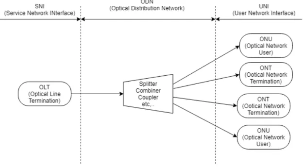
Communication in a PON is bidirectional between root and leaf, when taking the direction of root-to-leaf it is called downstream transmission and when it takes the opposite direction (leaf-to-root), it is called upstream transmission. With this example: root takes the name of Optical Line Terminal (OLT), which ensures information is being transmitted downstream and received upstream; leaf takes the name of Optical Network User (ONU),ensuring as-well that information is being received downstream and transmitted upstream; the branch is then named Optical Distribution Network (ODN) which consists on passive segments that contain any passive elements like optical fibres,splitters, combiners, couplers, filters and other optical components. More complex or composite ODNs, comprise of two or more passive segments interconnected by active devices.
According to [11] and in addition to the concepts above, there are also Optical Distribution Segment (ODS)s that represent a simple ODN comprised of an entire, passive, point-to-multipoint fibre structure, depicted in figure[2.1]. As well as OTLs, that represent passive
point-to-point segments of complex ODNs. Throughout literature in the matter, one may find the same meaning attributed to ONT and ONU, however, an ONT is actually an ONU that supports a single subscriber, while an ONU is an Optical Access Network (OAN) that terminates a leaf of the ODN and provides a User Network Interface (UNI).
Figure 2.1: Example of a simple ODN
2.1.2 Converging to an optical tomorrow - Environment Friendly tomorrow
Until a few decades ago, most of the wired communications were done via copper wires, optical fibre has changed that paradigm ever since it became available worldwide.
Optical communications is not a new subject as one might think... It has gained relevant ground compared to other wired communications due to constant research and development of tools and technology to bring it into the XXI century. The field of Optics, brings together at least three important Engineering groups: Physics, Materials and Electronics. Unlike copper wired based communications, optical communication resorts to the transmission of information through light(originated by a Light Amplification by Stimulated Emmission of Radiation (LASER) for example), being reflected throughout the core until it reaches its destination, but in order to avoid any losses, light is maintained inside the core through the total internal reflection phenomenon( with the cladding around the core having an inferior refraction index ) allowing the fibre to act as a waveguide.
that is reflected repeatedly on the surface of the fibre until it reaches its destination. Optical fibre brought a handful of advantages, such as the fact that it can provide higher rates of transmission(upstream/downstream) and higher bandwidth than copper. In addition, it can even have a longer reach, compared to copper and given the size and capacity of a single wire it allows an even bigger chance of scalability. In a single fibre,many services can be implemented by allocating a designated service to a specific channel to a target consumer thus providing higher capacity of coverage per user. Allowing so, scalability can be achieved in
the system, something that copper cannot provide correctly, without causing some noticeable changes in its structure.
With that being said, PON can be scalable over time reducing structure and maintenance costs over time far more easily than their counterparts, however, this leads to some of optics main disadvantages. Optical equipment can be expensive, complex and sensitive. Cost is mostly the reflection of the time-consuming process of designing, building and package these type of equipments. To produce optical fibre, for example, it requires combining different materials through various processes, further testing them with proper equipment, which adds to the final cost as well. Even upon completion, optical cables, should be handled with care, to prevent damaging the fibre inside and distort the signal being sent. Nowadays, there is a high demand for technology to be greener and environment friendly. This means that any new technology should take into consideration its overall impact towards environment and comes as no surprise that in a way, optical communication are slightly headed into that direction. As said above, although high equipment and manufacture costs, given the low number of active elements in the PON, resource and maintenance cost drop drastically since central offices across the network allow for more room and thus, more equipment. On a large scale, the more equipment you can place inside a cabinet for a longer time, means better management and maintenance and resource(water,electricity and rent) costs, which means less energy spent per equipment, leaning towards a greener use of technology,[12]. Plus, as decided by International Telecommunications Union (ITU) according to [13] each PON standard would carry over to the next in the way that, any new PON standard would be able to coexist with the previous and so on, which in turn, can imply that any equipment is capable of handling ”older” standards/equipment, reducing thus environmental foot print and reduce costs even further.
2.1.3 PON Roadmap
Full Service Access Network (FSAN) and Institute of Electrical and Electronics Engineers (IEEE) are some of the entities that regulate the optical spectrum and that stipulate the standards for future PONs. Once the first infrastructures for PON was laid, one of the most important goals for FSAN was that each new standard would have to provide compatibility with legacy PONs so that there would not be the need to often change devices and components, due to the consumer and producer costs. By having to re-invent a new device with each new emerging standard would prove too expensive for foundries for service providers and even for the users themselves since they would have to change their devices as well. To prevent this scenario, several roadmaps had to be laid out for the next decades dictating the goals for future PONs. Figure [2.2], demonstrates one of these roadmaps, starting from 2006 until 2015 more or less, guaranteeing the succession of GPON standard with New Gigabit Passive Optical Network 1 (NGPON1) also laying strategies for the upcoming NGPON2 standard.
Figure 2.2: PON Roadmap according to [14]
2.1.3.1 ATM Passive Optical Network (APON) and Broadband Passive Optical Network (BPON)
During the primordials of PON architectures (around the XX century), APON made a brief appearance around Europe as the first PON achieving significant commercial success, while being built over Asynchronous Transfer Mode (ATM). BPON came later, as an en-hanced version of its predecessor(APON), it added new features to the former PON such as dynamic bandwidth distribution and protection. It could also achieve speeds of up to 622Mb/s. Typically, these systems (APON/BPON) have a downstream capacity of 155 or 622Mb/s. Later versions would provide higher rates like symmetrical 622Mb/s downstream and upstream or asymmetrical 1.244Gbits/s downstream and 622Mb/s upstream.[5]
2.1.3.2 Ethernet Passive Optical Network (EPON)
Created in 2000 by IEEE, came to be EPON, that essentially was based on the Ethernet protocol and sending packets with different sizes, with the intent of extending Ethernet reach to access areas. So, The EPON has network capacities of symmetric 1.25Gb/s upstream and downstream. It achieved a reach of about 10km and a 1:16 split ratio.
2.1.3.3 Gigabit Passive Optical Network (GPON)
Created in 2001 by FSAN with the intent of increasing transmission rates and bandwidth. GPON came to be, being able to have one one case: a 2.5Gb/s downstream 1.25Gb/s channel upstream; but also allow the use of symmetrical 2.5Gb/s both ways. Slightly improving the EPON standard, it had a splitting ration of 1:64 and a reach of 10km as well.
2.1.3.4 New Gigabit Passive Optical Network 1 (NGPON1)
2.1.3.5 10Gigabit Passive Optical Network (XGPON) and 10Gigabit Symmet-rical Passive Optical Network (XGSPON)
Once again, in 2010, FSAN created a new standard: the NGPON1, that can be categorized by two modes XGPON and XGSPON. In the first mode XGPON, the PON can achieve 10Gb/s downstream and 2.5Gb/s upstream. The second mode is called XGSPON simply because it can achieve a symmetrical 10Gb/s upstream/downstream transmission. It has splitting ratios of 1:32/1:256 as well as a reach of about 20km to 60km.
2.1.3.6 New Gigabit Passive Optical Network 2 (NGPON2)
FSAN initiated the NGPON2 in 2010 but according to [15] efforts to push it forward started later around 2014. It follows the NGPON1 standard by being able to supply rates of 10Gb/s downstream and 2.5Gb/s upstream; or a symmetrical 10Gb/s upstream/downstream. But with access to Wavelength Division Multiplexing (WDM) technology spans these rates over 4 channels, being then able to achieve a total aggregate capacity per OLT of at least 40Gb/s downstream, 4*10Gb/s and 10Gb/s upstream, 4*2.5Gb/s, but potentially provide even higher capacities.
2.2
NGPON-2 - 40Gb/s capable PON
2.2.1 Characteristics and Requirements of NGPON-2
As explained in the section above, it was thought of NGPON2 implementation to be able to operate,(in an initial phase), at speeds of about 10Gb/s downstream and 2.5Gb/s upstream; 10Gb/s upstream and downstream over each channel. According to [13],[16], there are some target transmission rates of 160Gb/s downstream and 80Gb/s upstream, just not in this early stage of development.
The aggregate capacity of 40Gb/s is achieved through WDM, spanning regular NGPON1 rates over 4 wavelengths. However, according to [15], in 2012, FSAN agreed, and later standardized that the best technology for NGPON2 was TWDM due to technology maturity, system cost, loss budgets and complexity power consumption. Even though the technology didn’t exceed on any particular metric, its main advantage was simply being the best balanced, among other presented technologies.
NGPON2 is also expected to have a passive fibre reach of at least 40km and a maximum differential fibre distance, (difference between the nearest distance of an ONU to OLT and farthest distance of an ONU to OLT) of about 40km as well and it can also support a split ration of 1:256. With new PON systems, NGPON2 is expected to be flexible enough to balance trade-offs of speed over reach over split-ratios.
2.2.2 Migration
It was clear from the beginning of the layout/roadmap for future PONs and different standards, that each successive standard had to be compatible with all of the previous(Legacy PON). Because of this, all PON possess a Coexisting Element (CoE) to ensure coexistence of all legacy PONs over a new standard, guaranteeing the safeguard of all users. Plus it can also
allow for subscribers a Pay-To-Grow system, where they can adapt and pay an upgrade of their current service without the need to buy new equipment and without major changes in the network [12]. The figure below[2.3], shows a PON that can integrate an NGPON2 standard, whilst also being able to use other previous PON standards like GPON and NGPON1, over the same equipment over the ODN and distributing it to any different subscribers with different standards as well.
Figure 2.3: PON integrating multiple standards using a Coexisting Element, by [13] In reality there are a few different migration scenarios to meet specific needs in the network, and so, they may not be as flexible as was presented above, because they have to possess a certain balance to ensure smooth and seamless migration capabilities for subscribers.
There are at least two different migration scenarios, one of which, according to [13], is defined as PON greenfield migration scenario that comprehends that upgrading the overall structure takes time and a high investment. So with this in mind, an upgrade should only make sense when NGPON2 technology is sufficiently mature in order to completely replace copper systems or, as the name suggests deploy in a brand new area,(hence the name, green-field ). The main advantage for this deployment in a ”blank” area could benefit from higher bandwidth, split-ratios and other type of qualities that help provide and cover the expense of a newly built infrastructure whilst guaranteeing the same or even an enhanced bandwidth offer, than any other legacy PON, however, in this scenario, coexistence with other legacy PONs
is not a necessary requirement. Another migration scenario is defined as PON brownfield mi-gration scenario that is similar to the definition given above, where mimi-gration of subscribers from legacy PONs might be desirable, being able to replace legacy systems with NGPON2 completely in a relatively short time-frame. For this to happen, NGPON2 must coexist with legacy PONs over the same fibre and not requiring too much resources, likewise, services should not be interrupted for non-upgrade subscribers, if so, it should be as minimal as pos-sible. These possible migrations scenarios understand that coexistence, happens between 2 or three generations of PON. and when referring to legacy PONs, the following are being considered: GPON, XGPON, XGSPON, EPON and NGPON1.
2.2.3 System Requirements
Since, NGPON2 allows for scalability of the network, the number of potential equipment in it (the network) will increase as well. For the sake of good management and resources, all ONUs are designed to be colourless, not being bound to a specific wavelength. This means that they do not require the management of multiple ONU types by the OLT. According to figure [2.4] and [15],[16],[17], the 4 downstream channels of TWDM were placed near other legacy technologies wavelengths because of importance of coexistence in the new standard, and could potentially provide even minor changes in transmitters because the characteristics would be similar.
Figure 2.4: FSAN Wavelength Plan,[15]
Upstream however, there was interest in using the C-band, because it could prevent higher ONU costs. Another desired requirement was that, equipment should be tunable and colour-less, it simply was easier to provide some form of mechanism to synchronize and change a specific channel in a determined equipment, rather than having to build the same equipment for different wavelengths.
This information above is further complemented in table[2.1] with the assignment of each channel with its respective wavelength. The table focuses on the channels from first to fourth, despite having more wavelengths planned for future expansion.
Downstream Upstream Channels Wavelength (nm) Channels Wavelength (nm) 1 1596.34 1 1532.68 2 1597.47 2 1533.47 3 1598.04 3 1534.25 4 1598.89 4 1535.04
Table 2.1: Upstream and Downstream Channel Wavelengths [13] [18]
Since each of the four channels in TWDM is attributed to a given wavelength, in order to switch channels, any LASER or LED has to change its emitted output power to match that wavelength. This process requires precision and control in order for the power to not oscil-late and thus leave the required wavelength, incurring in rogue behaviour and malfunction. Furthermore, temperature also has a great impact regarding the former point, when the tem-perature rises, more current is required to achieve a certain emitted power compared to a lower temperature.
In addition, to ensure various deployment scenarios and network applications, NGPON2 should contain spectral flexibility to enable different subscriber demands and PONs over the same ODN. These diverse needs, will meet different requirements like jitter or delay, downstream/upstream ratios or even handling of launched power and sensitivity between OLT and ONU. Since one of the goals NGPON2 is conveying a more environment friendly type of communication, spectral flexibility allows power saving features over the network, where during non-peak hours, ONUs can retune to a common wavelength and allow OLT ports to be shutdown, [15]. Furthermore, it should also allow upgrading capacity of the network in a modular or progressive style,[19], like increasing the number of TWDM channel pairs according to different PON needs and so provide ease of coexisting between legacy PONs. To ensure resilience in the network, NGPON2 systems, will include redundancy equipment. The overall network topology could theoretically imply that if the central service OLT fail, every branch and leaf, respective ODS and ONU may fail as well [20]. By allowing a second OLT in the system, in case of a disruption, it will ensure that subscribers will not experience disturbances during their usage of NGPON2 technology. If disturbances do happen, it is expected for them to be somewhat short [12],[13],[15].
2.2.4 Transmission Convergence (TC) Layer
According to [21], the Transmission Convergence (TC) Layer is responsible for establish-ing communication protocols between the ONUs and OLT managestablish-ing so, multiple TWDM and Point-To-Point channels and wavelengths, which allows for Pay-to-Grow approaches, de-liver QoS over the network by identifying the channel number, the system it is operating (downstream) and also identifying which system the ONU is operating, as well as allowing Dynamic Bandwidth Assignment (DBA) to improve upstream TWDMPON bandwidth us-age by adapting to ONUs burst traffic patterns and so it may help provide either enhanced services or more subscribers.
Since it manages and establishes protocols between nodes inside the network it can identify the tuning of different ONU to OLT, keeping the respective FSMs up to date and checking new parameters for calibrations purposes, such as Physical Layer Operations Administration and
Maintenance (PLOAM) messages. Tuning identification can help the network to keep away rogue ONUs from disturbing communication, but regarding this topic, more is said below. Besides guaranteeing communication channels between nodes over the network, this layer is also responsible for framing its received bits and ensuring the correct message is decoded, all-the-while in vice-versa, it delivers the correct headers for the right destination. Which means that besides the standard decoding methodology, it can also include cryptography decryption as a mean for securing packets over the network. Figure[2.5] illustrates how this layer is organised into 3 other sublayers.
Figure 2.5: The 3 Sublayers of the TC Layer ,[21]
The TC layer, is composed of 3 sublayers: TWDM-TC framing sublayer ;TWDM-TC service adaptation sublayer and TWDM-TC PHY adaptation sublayer.
TWDM-TC service adaptation sublayer: Responsible for the upper layer Service Data Unit (SDU) encapsulation,multiplexing and delineation. Over the transmitting side, this sublayer accepts from upper layers, data frames and various control messages and performs SDU fragmentation if necessary, then it further assigns a XG-PON Encapsulation Method (XGEM) Port-ID and applies encapsulation to it, to obtain an XGEM frame, which can be optionally encrypted. Joining a few of these frames together form a payload to be sent down-stream or updown-stream. On the reverse side, the payload is received, then XGEM delineation is
applied filtered through Port-IDs and decrypts if necessary only then being able to reassemble the frames to their respective clients.
TWDM-TC framing sublayer: This sublayer is mainly oriented towards parsing or con-structing correct overheads of the frames in order to provide support to PON management. The sublayer formats are built so that frames and their elements are correctly aligned to specific boundaries, when possible.
TWDM-TC PHY adaptation sublayer: This sublayer is responsible for all the functions that might modify the bitstream, this is done to allow for better reception and transmission of the packets into the optical medium. The slight modifications might be done to the modulation of the optical transmitter, even introduce FEC or CRC in the bitstream.
2.2.5 Continuous and Burst Mode transmission
On this chapter, in the sections above, it was explained that communication following the direction from the root(OLT) to the leaf(ONU) was labelled as downstream communication and in the reverse direction, it was labelled as upstream communication.
In NGPON2 systems, OLTs are constantly turned on, actively monitoring and managing the network, whilst continuously sending information to its leaves(ONUs). When discussing reception however, OLTs can only listen to one ONU at a time, this means they have to multiplex through all devices, assigning a designated time slot for each one to communicate with the OLT. As a direct result of this, ONUs save more energy by having longer periods of no transmission(ie. LASER is turned off). Downstream transmission is continuous, meaning that the laser driving the optical signal is constantly turned on. In the case of upstream transmission however, it is done in burst mode, which implies that the laser driving the signal in the ONU is turning on and off; ”on” when the ONU is actively receiving and transmitting, and ”off” when it is in an idle/sleep state. Despite this, in downstream transmission, infor-mation/data is sent over periods of 125 microsecond windows and all ONU receive the same information. In burst mode, each ONU sends their information in a short burst during that given time frame, ensuring all the information from the ONUs arrive at the OLT.
The overall structure of a downstream frame consists of a downstream Physical Synchro-nization block(PSBd) with 24-bytes of size, followed by a payload which can of 38856 or 155496 bytes in size when the corresponding rates of transmission are, 2.48832Gbit/s and 9.95328Gbit/s respectively.
By the looking at figure[2.6], it shows that every ONU receives the same information from the OLT and that each downstream frame has a duration of 125 microseconds. The same way that downstream transmission carries a header in its frame (figure [2.7]), so does the burst frame, through the upstream Physical Synchronization block(PSBu), which consists of two elements: a Preamble and a Delimiter. The first is a known sequence that allows for the receivers Clock Data Recovery (CDR) unit to recover phase and frequency information, to sync data information with a recovered clock in order to process the arriving information.
Figure 2.6: Downstream Frame Structure. [21]
Figure 2.7: Upstream PHY Burst Header Structure. [21]
The figure below[2.8] represents burst frame transmissions from 2 ONUs to a single OLT. There are two distinct time intervals of 125 microseconds, when in the first both packets from the ONUs are fragmented, however only in the second time window, one burst frame is fully sent. This example symbolizes that despite a fragmented burst frame arrives at OLT, it can still be rebuilt and sent to its respective subscriber, confirming what we had previously learned in [21].
Chapter 3
Field Programmable Gate Array
(FPGA)
From a very generalist standpoint, FPGAs contain vast bidimensional arrays of transis-tors mixed with some other components ( that complement their performance ) that allow someone to easily and quickly build digital circuits, inside one device.
Inside a single chip, there are thousands of transistors, that can be arranged to create nu-merous digital circuits, so when combined or re-arranged they can perform logic or sequential operations that serve whichever purpose of the user. To create these digital circuits, FPGAs need to be programmed by the user with the help of Hardware Description Language (HDL) such asVHSIC Harware Description Language (VHDL) or Verilog. Optionally sometimes IP cores can be used to shorten the full code of a given project and provide a friendlier approach by connecting several of these blocks in a black-box approach [22].
Later these will use the created design to later be synthesized, implemented and programmed via a bit-file, generated by Software like Vivado or Altera Quartus ( In this project, Vivado is chosen as the software to be used ).
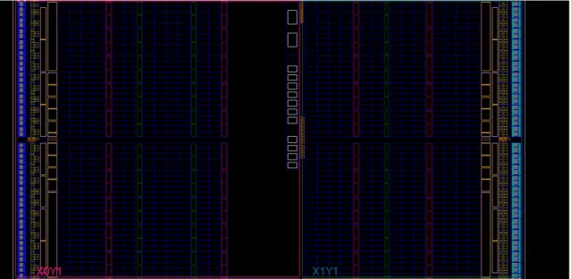
A regular FPGA is comprised of Configurable Logic Block (CLB), Input/Output Block, Embedded Memory blocks and Digital Signal Processing (DSP) blocks. Through figure[3.1] one can see two different quads(X0Y1 and X1Y1) containing these items separated by colour schemes: Memory Blocks (Red strips); DSP Blocks (Green Strips); CLBs (Dark Blue rectan-gles); Flip-Flops, Phase Locked Loop (PLL) blocks as well as input/output clock logic blocks (Orange strips and tiny Yellow Squares) and finally Input/Output Pads in (lighter blue than CLB’s) on both extremities of the image. All of these elements are interconnected through internal wires and other multiplexers.
![Figure 1.1: Moore’s Law: Calculations per second over time,[2]](https://thumb-eu.123doks.com/thumbv2/123dok_br/15822735.1081983/27.892.252.658.759.1018/figure-moore-law-calculations-per-second-over-time.webp)

![Figure 2.2: PON Roadmap according to [14]](https://thumb-eu.123doks.com/thumbv2/123dok_br/15822735.1081983/38.892.211.704.177.485/figure-pon-roadmap-according-to.webp)
![Figure 2.3: PON integrating multiple standards using a Coexisting Element, by [13]](https://thumb-eu.123doks.com/thumbv2/123dok_br/15822735.1081983/40.892.132.765.325.817/figure-pon-integrating-multiple-standards-using-coexisting-element.webp)
![Figure 2.4: FSAN Wavelength Plan,[15]](https://thumb-eu.123doks.com/thumbv2/123dok_br/15822735.1081983/41.892.127.776.603.896/figure-fsan-wavelength-plan.webp)
![Figure 2.5: The 3 Sublayers of the TC Layer ,[21]](https://thumb-eu.123doks.com/thumbv2/123dok_br/15822735.1081983/43.892.185.703.390.888/figure-sublayers-tc-layer.webp)
![Figure 2.6: Downstream Frame Structure. [21]](https://thumb-eu.123doks.com/thumbv2/123dok_br/15822735.1081983/45.892.189.708.197.479/figure-downstream-frame-structure.webp)
![Figure 2.8: Upstream PHY Burst Frame Structure. [21]](https://thumb-eu.123doks.com/thumbv2/123dok_br/15822735.1081983/46.892.204.685.184.472/figure-upstream-phy-burst-frame-structure.webp)