Universidade de Aveiro Departamento deElectr´onica, Telecomunica¸c˜oes e Inform´atica, 2018
Pedro Jos´
e
Do Couto Pissarra
Sistemas de Calibra¸
c˜
ao Autom´
atico para
Transceivers NG-PON2
Automatic Calibration Systems for NG-PON2
Transceivers
Universidade de Aveiro Departamento deElectr´onica, Telecomunica¸c˜oes e Inform´atica, 2018
Pedro Jos´
e
Do Couto Pissarra
Sistemas de Calibra¸
c˜
ao Autom´
atico para
Transceivers NG-PON2
Automatic Calibration Systems for NG-PON2
Transceivers
Disserta¸c˜ao apresentada `a Universidade de Aveiro para cumprimento dos requisitos necess´arios `a obten¸c˜ao do grau de Mestre em Engenharia Eletr´onica e Telecomunica¸c˜oes, realizada sob a orienta¸c˜ao cient´ıfica do Doutor Ant´onio Lu´ıs Jesus Teixeira e do Doutor M´ario Jos´e Neves de Lima, Professores do Departamento de Eletr´onica, Telecomunica¸c˜oes e Inform´atica da Universidade de Aveiro e do Engenheiro Francisco Rodrigues da PICad-vanced S.A.
o j´uri / the jury
presidente / president Professor Doutor Manuel Alberto Reis de Oliveira Violas Professor Auxiliar da Universidade de Aveiro
vogais / examiners committee Professor Doutor Ant´onio Luis Jesus Teixeira
Professor Associado com Agrega¸c˜ao da Universidade de Aveiro (Orientador)
Professor Doutor Henrique Manuel de Castro Faria Salgado Professor Associado da Faculdade de Engenharia da Universidade do Porto
agradecimentos Quero agradecer antes de tudo aos meus pais, Fernando e Anabela, e irm˜a, Diana, pela presen¸ca, for¸ca, dedica¸c˜ao, amor e educa¸c˜ao transmitida bem como, por todas as oportunidades que me proporcionaram com o intuito de crescer e definir o melhor caminho poss´ıvel.
Ao meu avˆo, Ant´onio, a quem infelizmente j´a n˜ao poderei partilhar este momento, e `a minha av´o, Maria da Luz, pelo amor, ternura, constante preocupa¸c˜ao e ensinamento. Um agradecimento especial aos restantes fa-miliares pelo suporte durante esta caminhada, mais concretamente ao meu tio, Alcides, e `a minha prima, Ana Celina, pelas brincadeiras e aventuras. Ao professor Ant´onio Teixeira e ao Engenheiro Francisco Rodrigues por me terem dado a oportunidade de desenvolver esta disserta¸c˜ao num am-biente empresarial, PICadvanced S.A., disponibilizando todos os recursos bem como aquisi¸c˜ao do esp´ırito de autonomia e confian¸ca proveniente dos restantes membros da empresa aos quais tamb´em agrade¸co.
Um especial agradecimento ao Dr.Engenheiro Ricardo Ferreira, pelo seu im-portante e indispens´avel contributo para o desenvolvimento da disserta¸c˜ao, demonstrando sempre disponibilidade e, em especial, paciˆencia e com-preens˜ao, transmitindo-me sempre uma for¸ca adicional para alcan¸car os objetivos delineados.
Quero agradecer tamb´em ao professor M´ario Lima e ao Engenheiro Fran-cisco Rodrigues, pela contribui¸c˜ao para a minha forma¸c˜ao, ao longo do meu percurso acad´emico, bem como durante a disserta¸c˜ao, ajudaram-me sempre que lhes solicitei ajuda.
Quero agradecer ainda `a S´onia, numa perspetiva pessoal, pela alegria, aten¸c˜ao, disponibilidade e preocupa¸c˜ao sempre com o pr´oximo, reunindo as mesmas valˆencias a n´ıvel profissional. Obrigado, professora S´onia, pelo de-terminante acompanhando acad´emico e pela excelente ajuda para o t´ermino do mesmo.
`
Aqueles com quem partilhei estes 5 anos, mais concretamente Filipe Costa, Jo˜ao Nuno Maciel, Alexandre Fontes, um muito obrigado por todos os momentos, aventuras bem como partilha de apontamentos, ideias, estudos e trabalhos. `A Maria Amaral, Catarina Gama e Carolina Fernandes, pela amizade, apoio e for¸ca para ultrapassar certos obst´aculos.
`
A pessoa que n˜ao me deixou ir ao fundo nestes ´ultimos 4 anos, por muito que escreva e escreva, nunca vou conseguir agradecer o suficiente por tudo que fez por mim, colocando tudo de lado para me tirar um sorriso. Obrigado por todo o caminho que j´a percorremos juntos e agradecer-te Adriana n˜ao ´
e um gesto que se p˜oe em papel, mas algo que se partilha ao longo da vida. Este trabalho ´e financiado pelo Fundo Europeu de Desenvolvimento Re-gional (FEDER), atrav´es do Programa Operacional Regional do Centro (CENTRO 2020) do Portugal 2020 [Projeto HeatIT com o nº 017942 (CENTRO-01-0247-FEDER-017942)];
Palavras-chave Comunica¸c˜oes ´Oticas, NG-PON2, Transceptores, FPGA, MGTs, SERDES, BERT
Resumo A sociedade atual depende cada vez mais dos servi¸cos de comunica¸c˜ao, exigindo melhores liga¸c˜oes e mais r´apidas, prevendo-se num futuro pr´oximo a necessidade de liga¸c˜oes na ordem das centenas de Gbit/s.
O aumento dos ritmos de transmiss˜ao refletem um aumento no que se refere `
a taxa de erro (BER), uma vez que o impacto associado a fatores como ru´ıdo ou interferˆencia entre s´ımbolos, ´e maior do que para baixos ritmos.
Este trabalho foca-se no desenvolvimento de um sistema de teste BER, tanto para uma transmiss˜ao cont´ınua como para transmiss˜ao em rajadas, que demonstre a viabilidade da comunica¸c˜ao sobre a tecnologia da pr´oxima gera¸c˜ao, Next Generation Passive Optical Network 2 (NG-PON2), que uti-liza d´ebitos de transmiss˜ao elevados (10 Gbit/s).
Para este efeito foi implementado uma arquitetura em Field-programmable gate array (FPGA) que possibilita para longas distˆancias na rede ´otica, elevados ritmos de transmiss˜ao. Esta escolha reflete uma alterativa mais econ´omica em rela¸c˜ao aos equipamentos comerciais e apresenta vantagens tais como a flexibilidade de reprogramar e preparar a arquitetura de acordo com as necessidades do utilizador.
Para cumprir os requisitos propostos o projeto dividiu-se em trˆes partes. Numa primeira parte do projeto desenvolveu-se uma arquitetura que permite adquirir a taxa de erros durante uma transmiss˜ao cont´ınua.
Com o intuito de analisar a viabilidade em tempo real da comunica¸c˜ao em quest˜ao, bem com o utilizador ter controlo sobre o sistema, alterando cer-tas caracter´ısticas do canal de comunica¸c˜ao, desenvolveu-se numa segunda parte do projeto uma interface entre o computador e a FPGA.
Numa ´ultima parte do projeto desenvolveu-se uma arquitetura semelhante `
a anterior, na qual se permite igualmente adquirir a taxa de erros com transmiss˜ao em rajadas (Burst), sendo este um dos requisitos de maior interesse na tecnologia NG-PON2.
Por fim, a prova de conceito foi realizada atrav´es de uma rede ´otica disponi-bilizada pela empresa PICadvanced, que permitiu a valida¸c˜ao das diver-sas partes do projeto. Estas valida¸c˜oes v˜ao permitir a conce¸c˜ao de novos m´odulos que posteriormente v˜ao contribuir para o projeto fonte que est´a em desenvolvimento na empresa PICadvanced, que visa a implementa¸c˜ao de uma placa de calibra¸c˜ao automatizada para os transceptores 10 Gigabit Small Form Factor Pluggables (XFP).
Keywords Optical Communications, NG-PON2, Transceivers, FPGA, MGTs, SERDES, BERT
Abstract The current society is increasingly dependent on communication services, requiring better and faster connections, predicting in a near future connec-tions in the order of hundreds of Gbit/s. During the data transmissions, the increase of speed reflects an increase of the error ratio due to factors such as noise, reductions of signal or jitter, which for low speed these were not emphasized so much.
This project involves the development of a BER test system for both con-tinuous and Burst mode of the transmission, demonstrating the viability of communication over the next-generation technology, NG-PON2, which uses high transmission rates (10 Gbit/s).
For this purpose, an FPGA architecture was implemented that allows for long distances in the optical network, high transmission rates. This choice reflects a more economical alternative in relation to commercial equipment and has several advantages, such as the flexibility to reprogram and prepare the architecture according to the needs of the user.
To achieve the proposed requirements, the project was divided into three parts. In the first part an architecture was developed that allows to obtain the error rate during a continuous mode transmission. In order to obtain the real-time viability of the communication referred and to have control over the system, an interface was developed between the computer and the FPGA to change certain characteristics of the communication channel. This is the second part of the project.
The last part of the project has an architecture similar to the previous one, that is, instead of the transmission to be done in continuous mode, it is performed in mode Burst, being this the requirement with more interest to the technology NG-PON2.
Finally, proof of concept was performed through an optical network provided by the company PICadvanced that allowed the validation of the different parts of the project.
These validations will allow the development of new modules that will later contribute to the main project that is under development in the company PICadvanced, which aims at the construction of an automatic calibration board for the XFP transceivers.
Contents
Contents i
List of Figures iii
List of Tables v
Acronyms vii
1 Introduction 1
1.1 General Framework . . . 1
1.2 Motivation . . . 3
1.3 Problem description and objectives . . . 4
1.4 Structure . . . 5
2 Concepts about the Next Generation Optical Networks 7 2.1 40-Gigabit-capable PON (NG-PON2) . . . 7
2.1.1 PON General Architecture . . . 7
2.1.2 NG-PON RoadMap . . . 8
2.1.3 NG-PON2 Standard . . . 9
2.1.4 Architecture . . . 9
2.2 Measurements and Figures of merit in NG-PON2 . . . 11
2.2.1 Burst Mode . . . 11
2.2.2 Laser Driving . . . 12
2.2.3 Tunable transmitter and receiver . . . 13
2.2.4 BER . . . 15
2.3 Transmission Convergence (TC) layer . . . 16
3 FPGAs for Calibration System - Technical Overview 21 3.1 Field-Programmable Gate Array (FPGA) . . . 21
3.2 Physical Layer . . . 23
3.2.1 Physical Coding Sublayer (PCS) . . . 23
3.2.2 Physical Medium Attachment Sublayer(PMA) . . . 23
3.3 Serial to Parallel and Parallel to serial conversion: SerDes . . . 24
3.4 High-speed serial data of FPGA KC705 . . . 25
3.5 Architecture of transceivers . . . 26
3.5.1 Transmitter . . . 27
3.5.3 Interface between the different clock signal domains of the transmitter 28
3.5.4 Interfaces with the Physical Layer . . . 29
3.5.5 Interface with the FPGA . . . 30
3.6 GTX Transceiver Structure . . . 31
4 Implementation and Results of BERT in Continuous Mode 35 4.1 Continuous Mode Communication Interface . . . 36
4.2 Bit Error Rate Tester (BERT) . . . 37
4.2.1 Bit Error Rate . . . 37
4.2.2 Idea of Operation of the BER Tester . . . 38
4.2.3 BER Tester . . . 39
4.3 Experimental Results . . . 44
4.3.1 Performance evaluation of upstream transmission . . . 46
4.3.2 Impact of System Sensitivity when using fiber . . . 47
4.3.3 Comparative study of the BERT system with a reference BERT system 48 4.3.4 Impact of Effect of Pre/Post-Emphasis Parameters . . . 48
4.3.5 Analysis of the Transmission Signal in the Optical Network . . . 49
5 Implementation and Results of BERT in Burst Mode 53 5.1 Burst Mode Communication Interface . . . 53
5.2 Burst Mode Architecture . . . 54
5.3 Bit Error Rate Tester (BERT) . . . 54
5.3.1 Block Diagram of system . . . 55
5.3.2 Explanation of the blocks . . . 55
5.4 Experimental Results . . . 56
6 Conclusion and Future Work 65 6.1 Conclusion . . . 65
6.2 Future work . . . 66
List of Figures
1.1 Global Mobile Data Traffic Drivers[2] . . . 1
1.2 Future PON network development[7] . . . 2
1.3 Automated board general project for XFPs calibration . . . 3
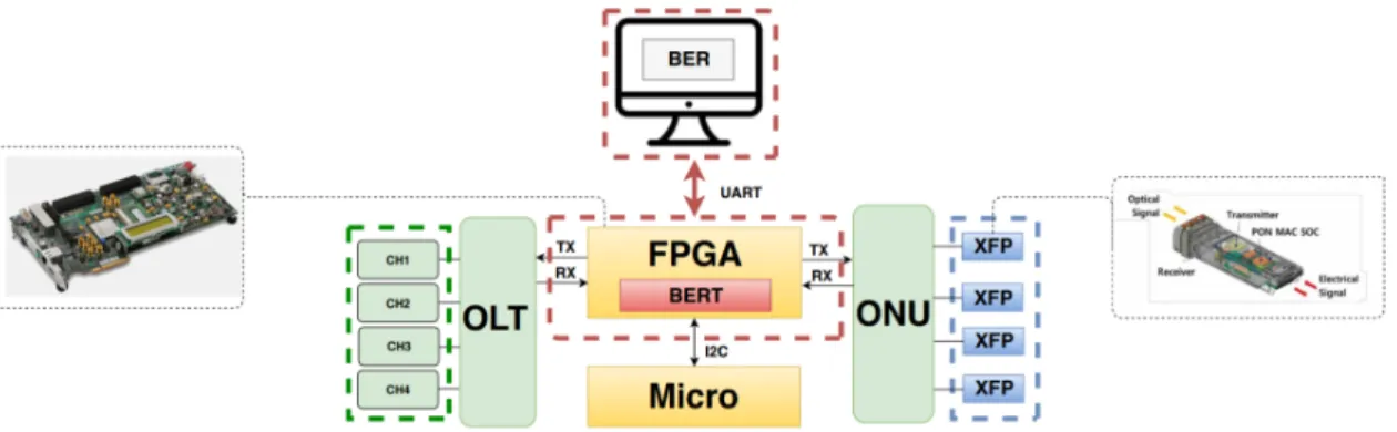
1.4 General diagram of the proposed problem . . . 4
2.1 Traffic between OLT and ONU [13] . . . 8
2.2 NG-PON2 roadmap [15] . . . 9
2.3 NG-PON2 roadmap [7] . . . 10
2.4 Data trace in Burst Mode Operation[22] . . . 11
2.5 Direct current modulation of a semiconductor laser[25] . . . 12
2.6 TWDM PON Wavelength tuning [29] . . . 14
2.7 Example of a structure transparent to a certain wavelength and reflective to others [31] . . . 15
2.8 Outline of TWDM TC information flow [16] . . . 17
2.9 Downstream PHY frame [16] . . . 18
2.10 Upstream physical synchronization block [16] . . . 18
2.11 Upstream PHY frame and upstream PHY bursts [16] . . . 19
3.1 A Configurable Logic Block used in FPGAs [11] . . . 21
3.2 Overview of FPGA architecture [11] . . . 22
3.3 The OSI reference model [38] . . . 23
3.4 SERDES Generic Block Diagram [42] . . . 24
3.5 GTX SMA Transceiver of Xilinx (KC705 Kintex-7) FPGA [41] . . . 26
3.6 General Architecture of Transceivers [40] . . . 26
3.7 GTX/GTH Transceiver TX Block Diagram [41] . . . 27
3.8 GTX/GTH Transceiver RX Block Diagram [41] . . . 28
3.9 Using RX Phase Alignment [41] . . . 29
3.10 Intersymbol Interference during a Transmission [42] . . . 30
3.11 Frequency and Datapath Relationship . . . 31
3.12 GTX structure provided by Xilinx generated in the VIVADO . . . 32
4.1 Description of the different stages of development performed during the project 35 4.2 Transmission of a byte . . . 36
4.3 Diagram of UART blocks developed in FPGA and interface developed in PC both for continuous mode . . . 37
4.4 Block diagram of 10 Gbit/s BER tester . . . 38
4.6 Diagram of logic function modules implemented in the FPGA . . . 40
4.7 Simplified block diagram of BERT in Continuous Mode . . . 42
4.8 Constantly reception of 32 bit data in parallel from the receiver . . . 43
4.9 Synchronization Block (INDEX = 16) . . . 43
4.10 Synchronization Block (INDEX = 32) . . . 44
4.11 Synchronization Block (INDEX = 48) . . . 44
4.12 Block diagram for the BERT system over the NG-PON2 technology . . . 45
4.13 Validation setup of the BERT system over the NG-PON2 technology . . . 46
4.14 BER as a function of received optical power for the different channels B2B . 47 4.15 BER as a function of received optical power for the different fiber length . . . 47
4.16 Comparison between the BERT system and reference BERT system . . . 48
4.17 System behaviour with Pre/Post-Emphasis parameter introduction . . . 49
4.18 Block diagram for transmission signal characterization . . . 50
4.19 Setup for transmission signal characterization . . . 50
4.20 Eye diagram results for the transmission tests . . . 51
5.1 Diagram of UART blocks developed in FPGA and interface developed in com-puter both for Burst mode . . . 53
5.2 Burst-mode traffic for the upstream transmission [52] . . . 54
5.3 Block diagram of the Burst-mode BERT . . . 55
5.4 Simplified block diagram of BERT in Burst Mode . . . 56
5.5 Behaviour of the different transmission signals of the Data Generator Block state 57 5.6 MGTs closed loop (blue SMA cable) . . . 58
5.7 Invalidate BER for Burst mode = 95 % . . . 58
5.8 Upstream PHY frame . . . 59
5.9 Upstream PHY frame that replaces the set of zero by preamble . . . 59
5.10 Upstream PHY frame expansion from preamble to 8000 bit . . . 59
5.11 System behaviour for different user defined Burst mode . . . 60
5.12 Behaviour of the different transmission signals signals of the Counter Block state 61 5.13 Upstream PHY frame expansion from preamble until the achievement of the synchronization . . . 61
5.14 Detailed PLL Block Diagram (adapted [55]) . . . 62
List of Tables
2.1 Relation between TWDM PON line rate options (adapted [10]) . . . 11 2.2 NG-PON2 tunning time classes[10] . . . 15 3.1 FPGA TX Interface Datapath Configuration (adapted [41]) . . . 30
Acronyms
B2B Back to Back
BER Bit Error Rate
BERT Bit Error Ratio Test BWmap Bandwidth Management CDR Clock Data Recovery CLBs Configurable Logic Blocks DFE Decision Feedback Equalizer
ER Extinction ratio
FPGA Field Programmable Gate Array
FS Framing Sublayer
FSAN Full Service Access Network FSM Finite State Machine
G-PON Gigabit Passive Optical Network
ITU-T Telecommunication Standardization Sector
LPM Low-Power Mode
LUTs Look-up Tables
MGTs Multi-Gigabit Transceivers
NG-PON Next-Generation Passive Optical Network NG-PON2 Next-Generation Passive Optical Network 2 ODN Optical Distribution Network
OFDM-PON Orthogonal Frequency Division Multiplexing PON
OLT Optical Line Termination
OMCI ONU Management and Control Interface ONT Optical Network Terminal
ONU Optical Network Unit
OPP Optical Power Penalty
OSI Open System Interconnection PCS Physical Coding Sublayer PHY Physical Interface
PISO Parallel in Serial Out
PLL Phase-locked loop
PMA Physical Medium Attachment PMD Physical Media Dependent PON Passive Optical Network PRBS Pseud Random Bits Sequence
PSBu Physical Synchronization Block appropriate for Downstream
ROM Read-Only Memory
SDU Service Date Unit
SerDes Serializer/Deserializes SIPO Serial in Parallel Out SMA SubMiniature version A TC Transmission Convergence TDM-PON Time Division Multiple
TDMA Time Division Multiple Access TEC Thermoelectric Cooler
TWDM Time and Wavelength Division Multiplexed Passive Optical Network
TWDM-PON Time and Wavelength Division Multiplexed Passive Optical Network PON
TWDM-TC Time and Wavelength Division Multiplexed Passive Optical Network Transmission Con-vergence
UART Universal Asynchronous
Receiver-Transmitter
VCO Voltage-controlled oscillator VOA Variable Optical Attenuator
WDM Wavelength Division Multiplexed WDM-PON Wavelength Division Multiplexed PON XFP 10 Gigabit Small Form Factor Pluggable XG-PON 10-Gigabit Passive Optical Network
Chapter 1
Introduction
This work occurs in the context of the development of the project conducted in the Curricular Unit Dissertation, within the study plan of the Integrated Masters in Electronic and Telecommunications Engineering. In this section, an introductory analysis of the project is made, from its general framework and the motivational point of view. Finally, a description of the problem, of its objectives and the structure of this dissertation is made.
1.1
General Framework
Over the past few years, the demand for high bandwidth has been increasing rapidly due to the emergence of advanced multimedia applications such as video services, online gaming, live streaming, ultra-High Definition and many other services, all of them competing for the same resources. Therefore, upgrading and developing new technologies is necessary to accommodate the new applications. The major topic of concern for telecommunication operators has been the increase of the bandwidth used by the end user[1].
According to Cisco’s Visual Networking Index (VNI), from 2016 until 2021 the total amount of data exchanged between mobile and users is expected to increase each year. This will create a networked society, and consequently a tremendous growth in mobile data will place huge pressure on operators. Figure 1.1 illustrates the global mobile data traffic required for next years [2].
Due to the technological advance, as well as the diversification of services and massifi-cation in internet access, there is a need for a modernization of telecommunimassifi-cation access network, particularly in the transition of Fiber technologies, since the requirement of a higher bandwidth and faster speeds are always present, challenging the limits of network capacity [3].
For the last years, operators have expressed interest in the implementation and develop-ment of Passive Optical Network (PON), to provide better service to users, such as high rate per client, as well as for providers once PON networks are attractive since they do not depend on active elements between their endpoints, allowing for reduction of maintenance costs and better operational efficiency [4].
PON technologies were standardized and developed across the world, but the increasing bandwidth demand makes the necessity for this type of network to evolve. Therefore, the current standardized technologies Giga-capable PON (G-PON) need to be upgraded to Next-Generation PON2 (NG-PON2), which is the next step on access network evolution and is currently on the process of study and standardization [5].
The NPON2 must co-exist on the same optical distribution network (ODN) of the G-PON, so it re-utilizes the already built infrastructures and consequently protects the initial investment and reduces the operation costs [5].
The full service access network (FSAN) group has been using the roadmap to guide the development of PON and according to them, NG-PON2 belongs to the next generation of PONs and is currently being standardised and is expected to be implemented in the near future [6]. Figure 1.2 illustrates the PON evolution.
Figure 1.2: Future PON network development[7]
The principle of NG-PON2 is to improve previous technologies, in terms of capacity, ODN compatibility, bandwidth and cost-efficiency. In April 2012, FSAN selected the Time Wavelength Division Multiplexing PON (TWDM-PON) technology as the best solution of choice for NG-PON2 [6][8].
Observing figure 1.1 and 1.2 it is possible to conclude that existing resources are not able to respond to this growing need for high-speed communications. Due to this it is urgently necessary to develop technologies, not only able to satisfy this demand, but at the same time to do it in an energetically and financially efficient way.
In this context the company PICadvanced appeared and has been responding increasingly with the pre-production of its 10 Gigabit Small Form Factor Pluggable (XFP)s for optical
network terminal (ONT) of NG-PON2 technology.
This pre-production is achieved through an automatic board that has been developed at PICadvanced in order to achieve automated calibration of the essential parameters for the final production of the XFPs.
Currently, the calibration board requires the development of some modules for the final step, allowing a greater productivity and yield in the production response of the XFPs, so that they can reach the final customer and consequently respond to the current needs of society.
1.2
Motivation
In the telecommunication market there must be standard for both the networks and the components, so that interoperability is achieved, and several manufacturers for the same technology [9]. The standard that PICadvanced follows for its transceivers NG-PON2 is the XFP that allows 10 Gbit/s in its data lines, which matches the specifications of the network standard [10].
Currently, the company PICadvanced has its XFP for ONT NG-PON2 pre-production and is in the final stage of the automated board development which allows the calibration of XFPs parameters, figure 1.3. As a way to increase its efficiency, this stage requires the implementation of test systems that will allow the control of the optical components and that will later be emulated in an optical network.
Therefore, one of the main requirements for this final stage is the addition of an FPGA to the calibration board referred, in order to implement an architecture for the automatic measurement of the BER levels of the system that will communicate, through inter-integrated circuit (I2C) with the microcontroller.
This microcontroller is already available in the current board and it coordinates all the test systems that aim at the production of the XFP, thus enabling the automation of the calibration board.
The achieved test systems are validated through a firmware environment developed to control the system as a whole.
1.3
Problem description and objectives
This project has as main objective the development of an architecture capable of providing to the microcontroller of the referred calibration board, the automatic measurement of BER levels in both directions, downstream and upstream.
The development platform used in this project is the Xilinx evaluation board KC705. It is equipped with an FPGA XC7k325TFBG900-2 device, provided with GTX transceivers supporting a line rate up to 10 Gbit/s.
Figure 1.4: General diagram of the proposed problem
Figure 1.4 illustrates the general design of the project to be carried out. To simplify its development, it was divided into 3 stages:
• Design and development of a bit error rate test (BERT) to a communication imple-mented in:
– Continuous Mode [11] – Burst Mode [12]
• Design of architectures that perform serialization and deserialization of data;
• Design and develop an interface so that the user may control the test system developed; The first part consists on obtaining an architecture in the FPGA of BERT system that allows evaluating the viability of the communication in future NG-PON2 technology.
This test system reflects on the underlying TWDM technology in the NG-PON2 that makes it possible to evaluate the communication when it is performed in a continuous mode, that is, when the communication is performed in a downstream direction between the op-tical line terminal (OLT) and opop-tical network unit (ONU), as well as the reverse direction, upstream, when communication is performed in Burst mode [6].
The second part of the project consists on the design of an architecture provided by the FPGA that allows the serialization and the deserialization of the data. This architecture convert the data from series into parallel, throught the deserialization process followed by the inverse process, serialization, that sends the data from parallel to series again, allowing it to be sent to the optical fiber network.
The third and final part of the project consists on an interface from the Universal asyn-chronous receiver/transmitter (UART) communication protocol between the FPGA and the
computer, in order to allow the control of the BERT system, by changing several parameters made available by the developed firmware application. Once the three parts of the project are completed, the final goal is achieved.
1.4
Structure
• Chapter 2: Concepts about the Next Generation Optical Networks It ex-plores important concepts about optical communications for the development of this dissertation. Initially, it gives an approach to the NG-PON2 standard and how the merit figures relate to the NG-PON2 transceivers, followed by the description of the transmission convergence layer that specifies the content of the different frame flows, for both downstream and upstream frames.
• Chapter 3: FPGAs for Calibration System - Technical Overview It present an overview of several aspects of the FPGA is presented, exposing the underlying ar-chitecture of the available transceivers Xilinx (KC705 Kintex-7) FPGA as well as some considerations relevant to the correct operation of the project in general.
• Chapter 4: Implementation and Results of BERT in Continuous Mode It describes the design and development of the all architecture and of interface related to the implementation of the BERT system in continuous mode. This chapter ends with several tests and results in order to get the concept’s proof of the architecture presented in 1.3.
• Chapter 5: Implementation and Results of BERT in Burst Mode It explores the previous architecture to reach Burst mode, describing the architecture changes re-quired for this mode to be achieved, approaching all issues and problems related to the Burst mode condition. Finally, the results are presented.
• Chapter 6: Conclusions and Future Work Presents a description of what was achieved, as well as the main conclusions taken from this project. Suggestions for more work on this topic are also presented.
Chapter 2
Concepts about the Next
Generation Optical Networks
2.1
40-Gigabit-capable PON (NG-PON2)
2.1.1 PON General Architecture
In order to support the high usage of bandwidth, optical communication networks that support high data rates had to be developed. Currently, in the access network, the optical communications architecture in use is based on Passive Optical Network (PON).
PONs have a topology that share point-to-multipoint (P2MP) architecture where all the elements should be passive, this is, without power supplies to operate. This architecture con-sists of the following main elements: the optical line terminal (OLT), the optical distribution network (ODN) and the optical network unit (ONU).
It uses a passive fiber tree topology to maximize the coverage, allow flexibility, and mini-mize the number of networking splitting, thus reducing the optical power loss and increasing the physical reach. The success of PON relies on its high bandwidth, infrastructure cost shar-ing, and simple maintenance and operation, which results from the absence of electronic active components between the OLT and the ONUs. Figure 2.1 presents each of the mentioned PON elements [6].
They are defined by the following[10]:
• OLT: Is the device located in the telecommunications operator terminal in charge of the management and maintenance of the ODN and its function is to transmit and receive data to several users. It sends the broadcast signal to all ONUs, controlling and synchronizing the data exchange in the access network.
• ONU: Is the device that terminates the network on the user side and receives the transmission signal from the OLT and then selects the data desired.
• Splitter: from the OLT, a single mode optical fiber is connected to the entrance of a 1: N passive optical splitter, where the N outputs of the splitter are connected to the ONUs of the clients via single mode individual optical fiber. This set of single-mode optical fibers and passive optical components that are installed between the OLT and end users, ONU, is called the ODN.
The two directions for optical transmission in the ODN are identified as follows:
• Downstream: Is the direction which the signals are transmitted from the OLT to the ONU. In this case, the OLT is the transmitter and the ONU is the receiver.
• Upstream: Is the direction which the signals are transmitted from the ONU to the OLT. In this case, the OLT is the receiver and the ONU is the transmitter.
In both directions of the transmission, Downstream and Upstream, the same components and optical fibers are used.
Figure 2.1: Traffic between OLT and ONU [13]
2.1.2 NG-PON RoadMap
FSAN group along Telecommunication Standardization Sector (ITU-T) are the forum standardization with the greatest activity in the study of PON evolution. The network operators have resorted to NG-PON solutions that can transparently coexist with legacy PONs on the existing fiber infrastructure and enable gradual upgrades in order to protect the investments [14].
Also, it is very important that coexistence on the same ODN is supported to satisfy cases where fiber resources are not abundant, and to minimize the interruption of service for users who are not migrating [6][14].
In addition, NG-PON must provide all G-PON legacy services in case of full migration and according to those entities, NG-PON technologies are divided into two parts: first stage NG-PON (NG-PON1), better known as 10-Gigabit Passive Optical Network (XG-PON), and second stage NG-PON (NG-PON2). NG-PON1 is known as the mid-term next generation based on 10 Gbit/s for both downstream and upstream directions [6].
NG-PON2 has been proposed by FSAN as a solution for new services applications, it is considered as the long-term generation of the optical access network which allows providing no less than 40 Gbit/s downstream and must remain backward compatible, figure 2.2 [15].
Figure 2.2: NG-PON2 roadmap [15]
2.1.3 NG-PON2 Standard
NG-PON2 is the response of network providers to increase the efficiency through the development of new services only possible with increase of bandwidth, especially the triple-play services, with voice, video, data, file sharing and online gaming that requires higher bandwidth capacity.
This technology is capable of offering higher capacity per customer than current G-PON and XG-PON1 systems, since it is a direct evolution of PON networks, which are a generation of independent PON systems based on the same transmission share part or all of the ODN through several dedicated wavelengths as form of protecting the service provider’s initial investment by taking advantages of the existing ODNs [15].
2.1.4 Architecture
PON2 is the latest of the ITU-T standardized PON system. The standard for NG-PON2 was defined by ITU-T in a series of recommendations G.989.x (x = 1, 2, 3) that define characteristics of the NG-PON2 system and the specifications from the Physical Media Dependent (PMD) and the Transmission Convergence (TC) [10][16][17].
The general requirements document (ITU-T G.989.1)[10] was approved in March 2013, addressing some requirements. Then in December 2014 (ITU-T G.989.2)[10] PMD specifica-tions were addressed. The last and most recent was approved in October 2015, addressing TC specifications.
Several technologies were suggested to support the requirements for the NG-PON2, such as 40G TDM-PON, wavelength division multiplexed PON (WDM-PON), time and wavelength division multiplexed PON (TWDM-PON) and orthogonal frequency division multiplexing PON (OFDM-PON) [18].
WDM-PON fails to adhere to the main requirements of NG-PON2, which is backward compatibility and, unfortunately, this feature is not available in this approach since it
re-quires wavelength selective optical ODN. 40G TDM-PON is also excluded due to the costs of implementation for each end user and the high chromatic dispersion over long distances. OFDM-PON, due to its need of time frame, which is a complex technology and its implemen-tation would have high costs as well as risks [18][19].
2.1.4.1 TWDM technology
Amongst these technologies, TWDM-PON has been selected as the best candidate for NG-PON2 and is supported by major telecommunication companies because it supports backward compatibility, flexibility and static sharing. It increases the aggregate PON rate by stacking XG-PONs via multiple pairs of wavelength. On a TWDM-PON architecture, four XG-PON networks are stacked by using four pairs of wavelength which are able to provide 40 Gbit/s and 10 Gbit/s as the present target and 160 Gbit/s and 80 Gbit/s as a future target for downstream and upstream, respectively [10].
Figure 2.3: NG-PON2 roadmap [7]
Figure 2.3, shows the architecture of the standard TWDM-PON system, which uses both WDM and TDMA. Typically, the architecture has a tree topology, with OLTs at the root of the tree and ONUs as the leaves, already between the OLT and the ONU, there is a new PON ODN (feeder fiber and power splitter) [10].
On the OLT side, a set of laser diodes, such as distributed feedback (DFB) laser diodes operating at different wavelength, serve as downstream laser source, followed by a WDM for multiplexing. The goal of the splitter used in ODN is to distribute power to all ONUs and consequently, each ONU would receive all wavelengths. Therefore, the ONU in TWDM-PON is equipped with a tunable transceiver, so it can selectively transmit or receive up-stream/downstream data on a pair of upup-stream/downstream wavelengths [20].
A tunable filter at the receiver is used to select or tune to any of the four downstream wavelengths. In case of upstream wavelengths, the tunable laser is used to provide colourless ONU [5].
Options to the baseline architecture include more pairs of wavelengths and different rates for stacking. TWDM-PON works with 4 – 8 channel pairs, each consisting of one downstream and one upstream wavelength channel, each channel pair should support nominal line rates of [6][10]:
Downstream (Gbit/s) Upstream (Gbit/s)
Basic Rate 10 2.5
Rate Option 1 10 10
Rate Option 2 2.5 2.5
Table 2.1: Relation between TWDM PON line rate options (adapted [10])
2.2
Measurements and Figures of merit in NG-PON2
There are several trade-offs between laser and receiver and, due to it, several figures of merit need to be checked in order to test the transceiver for characterization in NG-PON2. The figures of merit which require more attention for ONUs in this architecture are the Burst-mode operation, laser driving, tunability between four downstream and four upstream channels, and BER measurements.
2.2.1 Burst Mode
In TWDM-PON technology the downstream traffic is continuously broadcast to all ONUs, and each ONU selects the packets needed and discards the ones addressed to other ONUs and the upstream traffic of each ONU is only transmitted during pre-assigned time slots by the OLT, as illustrated in figure 2.4. A Burst mode transmitter requires the following features: fast Burst on/off speed, sufficient power suppression during idle period, and stable, accurate power emission during Burst transmission. These functionalities can be performed by specially designed laser drivers that are the most critical part of Burst-mode transmitters [21].
Figure 2.4: Data trace in Burst Mode Operation[22]
In conventional laser drivers, such as direct modulation, the bias current is maintained constant for continuous transmission. Burst mode operation requires the bias current to be
quickly turned on/off before/after Burst is transmitted. When an ONU is not transmitting, its laser is turned off and due to this, the temperature of the laser drifts and consequently wavelength is not the desired one [23].
Therefore, if the laser is turned off it is necessary to introduce a compensation into the driving circuitry in order to compensate the cooling and it will still be kept at the same temperature and wavelength that it had when transmitting. This compensation proves to be important because of the small spacing between the technology channels in NG-PON2. 2.2.2 Laser Driving
In high-speed optical communication systems the laser diode and modulator driver is one of the key components in the transmitter, where it performs the interface between high-speed electronics and the laser diode or modulator.
Therefore, the main goal of driving circuitry is to provide electrical power to the optical source and to modulate the light output in accordance with the signal that is to be transmit-ted. In semiconductor lasers, the bias current of the laser should be closed to threshold and then modulated by an electrical time-dependent signal. Thus, the driving circuit is designed to supply a constant bias current as well as modulated electrical signal [24].
The power at the output of a semiconductor laser depends on the current injected through the laser diode according to the power/current function represented in figure 2.5 [25].
When the population inversion is achieved, it means that the current reaches the threshold leading to lasing action. The laser output power then increases linearly with increasing current, until some saturation is reached for high bias current values.
Figure 2.5: Direct current modulation of a semiconductor laser[25]
According to the modulating signal, the laser driving current is assorted resulting into modulation of the emitted power. The modulation optical signal is represented at two different values of the bias current, but an increase in the bias and modulation currents of the laser will increase its output power, resulting in improved dynamic behaviour.
It is important to notice that the laser threshold increases and the power/current function efficiency decreases as the operating temperature goes up. The laser threshold is sensitive to the operating temperature and the bias level control is needed [25].
Extinction ratio (ER) is an important parameter included in the specification of most fiber optic transceivers. It can affect the performance of digital optical communication systems because it transmits binary data using two levels of optical power, where the higher power level represents a binary 1 and the lower power level represents a binary 0. These two power levels can be represented as P1 and P0 where P1 > P0 and the units of power are watts [26]. For a constant temperature the transfer function stays the same, meaning that if bias current were to change, the ER would decrease with the increase of the power of the zero, and ER is given by:
ER (db) = 10log(P 1
P 0) (2.1)
Changes in the driving current of the laser influence its output power and the maximum allowed power to the standard, needs to be between 4 dBm and 9 dBm upstream direction [10].
• Too much power may cause non-linear effects in the fiber.
• Too low power may produce lacking BER and sensitivity merit figures.
It is necessary to be careful with the increase of the driving current of the laser since it may diminish the ER of the optical fiber and may cause it to become lower than the minimum of 6 dB, which is set by the standard. A lower value of ER will require more optical power penalty which indicates how much more power is needed in the input of the receiver to ensure the same error probability, being this a feature defined by standard, and the value is between 1 and 2.
2.2.3 Tunable transmitter and receiver
In TWDM-PON system wavelength-tunable ONUs are implemented, which realize sev-eral attractive functions, such as the load balancing, power saving and colourless ONU, and redundancy [27][28].
• Load balancing:
– It happens when the ONU communicates with an OLT using the wavelength ini-tially allocated by the OLT. The OLT orders ONU to change its wavelength to another empty wavelength when traffic concentrates on one wavelength.
• Power saving:
– ONU power consumption can be adequately decreased by the power-saving func-tions. The OLT side power saving can happen during the time of low traffic load (for example overnight) as all ONUs on an ODN can retune to a common wave-length and allow OLT ports to be powered down.
• Colourless:
– The colourless ONU means that all ONUs in the system have the same speci-fications and are wavelength-independent that allow reduced manufacturing and operation costs derived from inventory reduction (management), flexibility.
• Redundancy:
– ONU can change the wavelength to connect to a healthy OLT if the original OLT fails. Appropriate specifications to realize this are expected.
Figure 2.6: TWDM PON Wavelength tuning [29]
Therefore, the ONUs are equipped with tunable transceivers and tunable receivers that function as selectors to any of the four upstream and downstream channels. For each ONU transceiver to be able to tune its reception to one of the downstream wavelength and its transmission to the corresponding upstream wavelength, it is necessary to employ different filters locked to a specific wavelength in each ONU, as shown figure 2.6. [30][29]
So, the transceiver must be able to change the laser parameters in order to allow the wavelength of the spectrum to change to another channel. The main goal of the laser is allowing a change in the band that the photodetector receives, that is, that filters the incoming optical signal to the band desired [30].
It is usually used as a tunable optical filter, the component shown in 2.7, composed of a single cavity and two distributed Bragg reflectors (DBR). The refractive indices of optical layers vary by controlled temperature, shifting the transmission wavelength of the filter.These changes in temperature can be achieved with a thermometric cooler (TEC). It allows to change and maintain a set temperature, and consequently its wavelength, allowing it to tune to a specific channel in architecture with more than one wavelength, like NG-PON2.
Figure 2.7: Example of a structure transparent to a certain wavelength and reflective to others [31]
One important aspect in NG-PON2 is the tuning time between channels. There are three classes for the wavelength channel tuning time of the ONU transmitter and receiver that are specified in NG-PON2 as shown in table 2.2.
Classes Tuning Time 1 < 10 µs
2 10 to 25 ms
3 < 1 s
Table 2.2: NG-PON2 tunning time classes[10]
2.2.4 BER
BER measurements are used to assess systems that transmit digital data from one location to another.
When data is transmitted over data link, there is a possibility of errors introduced into the system, such as, noise, interference, and phase jitter may cause degradation of the digital signal which affects the integrity of the system [32][11].
Therefore, it is necessary to evaluate the performance of the system and this can be achieved by means of BER measurements. It enables to assess if communication can be supported or if it is difficult or even impossible, rather than testing the component parts and hoping that they will operate satisfactorily when in place.
BER can be defined as the rate at which errors occur in a transmission system. The following equation 2.2 shows the ratio between the number of errors that occur in a string of a stated number of bits [33].
BER = ReceivedBits with errors
T otal number of bitstransmitted (2.2) For a fiber optic system, bit errors essentially result from imperfections in the components
used to make system connections, such as the optical driver, receiver, connectors and the fiber itself, but it can also be introduced as a result of optical fiber dispersion and attenuation [32]. In what concerns the receivers, the sensitivity is defined as the minimum optical power required to achieve a specific BER. The number of errors at the output of decision circuit will determine the quality of the receiver and, of course, the quality of the transmission system [34].
In NG-PON2 the merit figure for BER is that the sensitivity, that is the power at which the BER = 1 × 10⁻³must be equal or lower than -28 dBm for downstream and -26 dBm for upstream, only to Type A link at 10 Gbit/s [10]. An additional requirement is that power penalty of the 20km of fiber, that is, the difference between sensitivity with or without fiber what is called optical path penalty (OPP), must be lower than 2 dB for downstream and 0.5 dB for upstream [10].
2.3
Transmission Convergence (TC) layer
The transmission convergence (TC) layer is the protocol layer of the NG-PON2 system that is positioned between the PMD layer and service clients. More details will be presented in the following chapter. It builds on the XG-PON recommendations [35], with modifications for NG-PON2’s specific features. This subsection was made according to [17].
A NG-PON2 system may contain a set of TWDM channels, a set of point-to-point wavelength-division multiplexing (PtP WDM) channels or both. Each technology uses a different TC layer and only the first will be described in this subsection.
The TWDM-TC layer is a part of the TWDM-PON protocol stack that specifies the formats and procedures of mapping between the upper layer services data unit (SDUs) and bitstream suitable for modulating the optical carrier.
This layer is composed by three sublayers, which are, service adaptation sublayer, framing sublayer and physical adaptation sublayer. It is also responsible for functions such as the per-formance monitoring, security key management, ONU power management, TWDM channel management and protection.
TWDM-TC layer is present in both the OLT and the ONU side. In downstream direction, the interface between TWDM-TC and PMD layers is represented by the bitstream divided into the frames of 125 µs duration. In the upstream direction, the interface is represented by the series of precisely-synchronized time-bursts.
With the help of figure 2.8, the three layers mentioned will be focused on, referring to some essential blocks and properties in a brief way.
• TWDM-TC service adaptation sublayer:
– Is responsible for the upper layer SDU encapsulation, multiplexing and delineation. This layer deals with two types of SDUs such as user data frames and ONU Man-agement and Control Interface (OMCI) messages that decompose logically in a XG-PON Encapsulation Method (XGEM) engine and two service adapters: the user data adapter and the OMCI adapter. The user data adapter can also be configured to accommodate a variety of upper layer transport interfaces.
• TWDM-TC framing sublayer:
– Is responsible for the construction and managing the fields necessary for the data-stream management in PON. The TWDM-TC framing sublayer formats are de-vised so that the frames, bursts and their elements are aligned to 4-byte word boundaries, whenever possible.
• TWDM-TC PHY adaptation sublayer:
– provides function to modify the data-stream modulated by the optical transmitter in order to improve the detection and sensitivity. It also describes the properties of the signal transmitted through the optical medium and secures the data by the error-coding techniques.
Figure 2.8: Outline of TWDM TC information flow [16]
During this project there will be the need to work on the TWDM physical layer and due to this it is important to understand what this layer essentially contains and what its requirements for its ideal operation are. Therefore, within this layer there are two essential frames such as downstream PHY frame and upstream PHY frame, which will be the frame explored during the last part of the project.
The downstream transmitter of the OLT operates in continuous mode at one of two possible line rates: 9.95328 Gbit/s or 2.48832 Gbit/s.
A downstream PHY layer frame consists of physical synchronization block appropriate for downstream (PSBd) and a PHY frame payload, figure 2.9. The PHY payload is represented by the downstream FS frame whose content is scrambled and optionally protected by forward error correction (FEC), it can be turned on or off depending on the operational considerations.
Figure 2.9: Downstream PHY frame [16]
The ONU upstream transmitter operates in the Burst mode at the nominal line rates of 9.95328 Gbit/s or 2.48832 Gbit/s. In the upstream direction, each ONU transmits a series of relatively short PHY bursts and remains silent, disabling the transmitter in between the bursts.
At the PHY layer, each upstream ONU burst contains the physical synchronization block appropriate for upstream (PSBu) and an upstream FS frame containing a header used for identification, status indication and series of individual allocations, among others.
For each upstream ONU transmission burst, the BWmap in the downstream FS frame specifies the start time of the burst and the size for individual allocations within the burst so that the upstream transmissions by different ONUs are non-overlapping.
The PSBu, figure 2.10, contains a preamble and a delimiter. The preamble and the delimiter are employed by the optical line terminal channel termination (OLT CT) Burst mode receiver to determine the presence of a PHY burst and delineate the PHY burst. According to [16], the recommended size of the preamble and the delimiter is 160 bits and 32, respectively.
Figure 2.10: Upstream physical synchronization block [16]
Observing figure 2.9 it is possible to conclude that the transmission of OLT is split into fixed size downstream PHY frames, while in figure 2.11 each ONU transmits a series of bursts of different sizes. Both transmission frames have a duration of 125 µs, which corresponds to the maximum size of 38880 bytes at the rate of 2.48832 Gbit/s, and to the maximum size of 155520 bytes at the rate of 9.95328 Gbit/s.
Chapter 3
FPGAs for Calibration System
-Technical Overview
3.1
Field-Programmable Gate Array (FPGA)
FPGAs, are integrated circuits containing logic which can be programmed by the user in the field [11]. Logic blocks contain a wide set of programmable logic gates and memory elements (simple flip-flops or more complex block of memories). FPGAs also contain inter-connection resources, which allow the blocks to be wired together and to implement almost any kind of digital circuit or system. [11][36] The logic described in hardware description lan-guage (HDL) such as VHSIC Hardware Description Lanlan-guage (VHDL) or Verilog can later be synthesized with software that also implements the design and generates a bit-file which describes how the configurable logic blocks (CLBs) and interconnections are to be configured (to implement the desired logical functions) [11].
Figure 3.1: A Configurable Logic Block used in FPGAs [11]
The interconnections and look-up tables (LUTs) are configured by 1-bit memory cells, mostly static random access memory (SRAM) based, which make certain connections to CLBs and make LUTs hold certain values. The LUTs can implement all combinational logical functions, i.e., OR, AND, NOT, XOR and their complements as well as any custom behaviour. Figure 3.1 shows an example of a CLBs. CLBs can contain full adders (FAs) for accelerating addition and subtraction and some FPGAs contain special a digital signal processing (DSP) block for more complex mathematical operations, such as multiplication
and division. There are also multiplexers (MUXes) for routing the signal and a d-type flip flop (DFF) for saving one bit [11][36].
The basic structure of an FPGA, figure 3.2, includes the following elements [11]: • Look-up Tables: block which performs logical operations;
• Flip-Flops: register elements which can store the result of the LUTs; • Wires: interconnection resources;
• IO pads: physical ports that get data in and out of the FPGA.
Although this structure allows the implementation of a wide range of digital systems in order to improve their efficiency, contemporary FPGAs incorporate additional elements, which implement specific functions such as [11]:
• Embedded memories to distribute data storage (Block RAMs);
• Phase-locked loops (PPLs) to drive the FPGA fabric at different clock rates; • External and/or embedded microprocessors;
• Digital Signal Processors (DSPs).
3.2
Physical Layer
The open system interconnection (OSI) reference model shown in figure 3.3, was developed by the International Standards Organization (ISO) and defines seven layers in network com-munication systems. Physical layer in context is the lowest in the hierarchy and is concerned with physical transmission of data over various transmission mediums, such as cabling, fiber optics or wireless. The Application layer is presented to users and the layers in between take care of, e.g., routing data packages over the Internet. The Physical layer includes mechanical, electrical and timing interfaces in its design to make the transferring of bits as accurate as possible. Due to its complexity it can be described by other sub-layers [37].
Figure 3.3: The OSI reference model [38] 3.2.1 Physical Coding Sublayer (PCS)
The physical coding sublayer lies below the data link layer (layer two) in the OSI refer-ence model and above the physical medium attachment (PMA) physical sublayer. The PCS performs several functions, such as the encoding/decoding and scrambling/descrambling of data blocks. The encoding of data is performed together with scramblers to ensure enough transitions between logical ones and zeroes so that the receiver can perform clock recovery from a serial link which provides no clock reference. The PCS can insert and remove mark-ers for the alignment of data and can identify blocks of received data streams for encoding schemes, such as 8B/10B [39][37].
3.2.2 Physical Medium Attachment Sublayer(PMA)
The physical medium attachment sublayer connects the PCS to an electrical interface, such as an optical transceiver. Receivers are essentially photo-detectors connected to circuits for amplification and quantization, often sharing any controlling circuit with the transmitter. For high-speed links, the PMA serialized/ deserialized data performs clock recovery from received data streams. The PMA is responsible for taking inputs of parallel data and sending it out at high speed (and vice versa), and the data conversions can be implemented in a Serializer/Deserializer (SerDes) circuit, which is described in the following section. [40][37]
3.3
Serial to Parallel and Parallel to serial conversion: SerDes
The increasing requests for reliable high-speed transmission over long distances has often made serial link preferred over parallel ones. However, since data elaboration is often parallel, data needs to be serialized on the transmitter side and deserialized on the receiver side [41].
A specialized circuit for doing this conversion has been projected and is constantly devel-oping, it is called SerDes. The working principle of a “SerDes” is relatively simple because a parallel data is clocked into the parallel register synchronously to a slow clock and shifted out, one bit at a time, at a higher serial clock rate. These blocks are often called “parallel in serial out” (PISO) and the inverse operation is called “serial in parallel out” (SIPO)[42][41]. Basically, there is a shift register which receives data one bit after the other and transmits its contents to a storage register used to hold the data for the slower, parallel clock. This scheme can only work well if the transmitter and receiver clocks are perfectly synchronized.
Figure 3.4: SERDES Generic Block Diagram [42] Description of each block of the Serializer diagram [42]:
• Transmit FIFO (First IN, First Out):
– Storing the incoming data before transmission. • Line Encoder:
– This is an optional block sometimes not included in a SerDes. It encodes the data into a more line-friendly format and usually involves eliminating long sequence of non-changing bits. It may also adjust data for an even balance of ones and zeros. • Serializer:
– This is a block that serializes the received data, that is, when it receives a certain number of data in parallel (x data) at a given rate (frequency y), it transforms it into a given stream at a rate of x multiplied by y.
• TX Line Interface:
– This block turns out to be the final interface of the Serializer with physical cable, and generally it also allows better recovery of the receive-side signal.
Alternatively, the Deserializer must do the whole inverse process that the block Serializer does. The functions of each block are briefly described below [42].
• Rx Line Interface:
– It is the interface of the Deserializer with the physical cable. It can use some passive or active signal equalization.
• Deserializer:
– Converts the serial data it receives at a rate of x multiplied by y, in x data parallel to a cadence of y.
• Line Decoder:
– Decodes data received. • RX Elastic Buffer:
– Aligns the incoming data into the proper word boundaries. Several different mech-anisms can be used for automatic detection and alignment of a special reserved bit sequence.
• Clock Correction and Channel Bonding:
– This block allows the correction of differences between clock signals and correction of delays between different channels (if there is a multi-channel transmission). There is also a block that is common to both the serializer and the deserializer which is the Clock Manager, which is essentially responsible for the various processes that the clock signals need: from frequency multiplication, division and even retrieval [41][42].
This architecture presents the essential blocks for the proper functioning of a serializer and deserializer, however there are other features that can be added: from the different types of possible encodings to detector codes and error correctors that can be added to the architecture. [42]
3.4
High-speed serial data of FPGA KC705
Xilinx Series 7 FPGAs have transceivers capable of high-speed serial communication as required in this project.
Specifically, according to [40], GTX transceivers are available in the Xilinx (KC705 Kintex-7) FPGA which allow a speed of 12.5 Gbit/s. In other models there are other transceivers, such as GTZ (allowing up to 28 Gbit/s), GTH (which allows rates up to 13.1 Gbit/s) and GTP (with debits up to 6.6 Gbit/s). However only the GTX transceivers will be addressed, since they are the most suitable ones for this type of communication and the only ones available in the FPGA used.
In figure 3.5 shows the FPGA to be used in the project and the entries/exits of the GTX SMA Transceiver which will be used for concept’s proof.
Figure 3.5: GTX SMA Transceiver of Xilinx (KC705 Kintex-7) FPGA [41]
3.5
Architecture of transceivers
The GTX transceiver is essentially a high-speed SerDes developed by Xilinx for Kintex-7 family FPGAs. It is a highly power-efficient configurable module that can produce line rate up to 10 Gbit/s. The GTX transceivers are grouped into four channels described as Quad and these are strategically close in order to minimize the layout size and power consumption [41].
Each GTX transceiver is composed by transmission block (TX) and receiving block (RX) and the figure 3.6 shown the general architecture of FPGA transceivers.
Figure 3.6: General Architecture of Transceivers [40] Its architecture is briefly described, according to the [40] and [41]:
As you can see from the figure, there are two sublayers (PMA and PCS) which have already been mentioned above.
Each sublayer provides different blocks. The PMA sublayer includes: Serial/Parallel (PISO and SIPO), Phase-locked loop (PLL), Clock Data Recovery (CDR) and Pre/Post-emphasis and provides equalization programming to optimize the received signal integrity.
On the other hand, PCS sublayer includes: 2-byte and 4-byte internal data path to support different line rate requirement, pseudorandom binary sequence (PRBS) generator/checker,
8b/10b encoding/decoding protocol, comma detect and alignment and equalization blocks, among others. Following these sublayers there is FPGA logic interface.
3.5.1 Transmitter
In figure 3.7 the architecture of the GTX transmitter is shown. It has blocks with different functions that allow to maintain the integrity of the signal during a transmission. The data flows from the right side to left side.
Figure 3.7: GTX/GTH Transceiver TX Block Diagram [41]
The block on the right, TX PCS, is the FPGA TX interface, where the parallel data input of the FPGA will be serialized. The users can define their own TX data pattern in this block, such as utilization of memory or coded-pattern generators as well as the width of TX data (2-byte, 4-byte), according to [41].
Parallel data enters this block at a given well-defined cadence: to the positive edge of the TXUSRCLK2 clock signal, this being the synchronization signal between the data coming from FPGA and the transmitter. However, another clock signal is also required for the PCS internal logic of the transmitter: TXUSRCLK. [41]
The TX data and control signals in this block are running under TXUSRCLK domain (typically below 500MHz). Bear in mind that the PCS internal logic works with the data in parallel, so the value of this clock signal depends, not only on the cadence at which the data enters the transmitter, but also on the chosen datapath.
The PCS block uses two clock signals internally for its correct operation: TXUSRCLK (as already mentioned) and XCLK (parallel data clock signal of the PMA block). Figure 3.7 illustrates the different clock domains present in the GTX transmitter.
When the data is transferred between the TXUSRCLK and the XCLK domains, it is necessary that in addition to having similar frequencies, any phase differences that may exist are resolved. This will be focused on with more detail in subsection 3.5.3.
Lastly the TX PMA block is basically composed by a high-performance serializer and a configurable driver. The PISO block, parallel in and serial out, uses the high-speed serial clock (typical several GHz) to sample coming parallel TX data for serialization [41].
3.5.2 Receiver
In figure 3.8 it is possible to see the architecture of the receiver GTX, that includes several blocks which allow the correct recovery signal, being the operating of certain blocks already mentioned in the subsection 3.3.
The RX actually performs the opposite of the TX side. As the figure 3.8 shows, the data flows from left to right in RX block. Similar to TX block, each RX contains RX PMA and RX PCS blocks. The RX PMA is composed by a high-performance receiver, programmable equalizer, CDR and SIPO block.
Figure 3.8: GTX/GTH Transceiver RX Block Diagram [41]
The two programmable RX equalizers including decision feedback equalizer (DFE) and low-power mode (LPM) help the CDR circuit to recover received high-speed data stream. These equalizers are selected depending on the system level trade-offs between power and performance.
For a lower-loss channel, LPM mode is chosen for power efficiency. On the other hand, for equalizing high-loss channels, the DFE mode is selected to offer better data recovering quality. The parallel data then flows into the RX PCS block. This RX data usually shares the same bit width with TX data which can be configured by FPGA TX/RX interface block [41].
Also, the comma detect is presented to align the input signal accordingly. These processes are under parallel clock RXUSRCLK domain which is the duplication of TXUSRCLK. The RX PCS block also has built-in loopback paths to receive parallel TX data from TX PCS and the ability of transmitting received data to TX PCS. After passing these blocks, the processed parallel RX data is then provided to the FPGA RX interface [41].
3.5.3 Interface between the different clock signal domains of the transmit-ter
The PCS block uses two clock signals internally for its correct operation: TX/RXUSRCLK (as already mentioned) and XCLK (parallel data clock signal of the PMA block).
All this functionality also occurs on the receiver side since it operates in different clock signal domains. Figure 3.7 illustrates the different clock domains present on the GTX receiver.
When data is transmitted from one domain to another, all phase differences between the clock signals must be resolved and the frequency should not change much. For this reason, one of the following two blocks must be used: the elastic buffer or the phase alignment block. Both blocks solve the phase differences between the two domains, however they present their advantages and disadvantages.
On the one hand, according to [41], the buffer is a robust structure and easy to operate, whereas the phase alignment block requires more logic and restrictions regarding the clock sources. But the use of the buffer implies a higher latency since the phase alignment block is designed to decrease the total latency of the system.
Figure 3.9: Using RX Phase Alignment [41]
3.5.4 Interfaces with the Physical Layer
The interfaces with the physical layers on both sides of the transmission (receiver and transmitter) include analog circuits that allow transmitting and receiving differential signals. However, the signal communicated along the channel may be subject to interference for several reasons which are critical in receiving the signal [43].
Therefore, techniques implemented in these same interfaces are used which, on one side, are responsible for ”preparing” the signals to be transmitted to a noisy channel, in order to prevent their change, and, on the other side are responsible for correcting the data received according to certain characteristics.
These techniques are referred to as Pre-Emphasis on the transmitter side and Equalization on the receiver side [42].
During transmission on the physical channel it is normal to have the phenomenon of Inter-symbol interference (ISI), figure 3.10 that occurs due to the fact that there are long periods of transmission of a certain value followed by a short period of time with an opposite value.
Figure 3.10: Intersymbol Interference during a Transmission [42]
It is important to control this type of interference and because of this the physical chan-nel uses the pre-emphasis/de-emphasis technique. According to [42] it is one of the most important characteristics of the interface with the physical layer, consisting of an intentional overdriving at the beginning of a transition and an underdriving on the consecutive bits that present the same value.
This way, when the phenomenon of intersymbol interference occurs, the capacity of the channel to recover the full amplitude of a small transition will not become a problem.
3.5.5 Interface with the FPGA
Just like in the transmitter there are two clock signals required for the correct operation of the receiver: RXUSRCLK e RXUSRCLK2. The clock signal RXUSRCLK is the internal signal for the logic of the PCS block (which handles the data in parallel) and the second which has already been mentioned as the synchronism clock signal between the receiver and the FPGA logic. It is important to remember that the PCS internal logic works with data in parallel, so the value of this clock signal depends, not only on the cadence at which the data enters the transmitter, but also on the chosen datapath.
TX INT DATAWIDTH Internal Data Width FPGA Interface Width TXUSRCLK2 Frequency
0 (2 bytes) 16 16 FTXUSRCLK2 = FTXUSRCLK
0 (2 bytes) 16 32 FTXUSRCLK2 = FTXUSRCLK/2
0 (2 bytes) 20 20 FTXUSRCLK2 = FTXUSRCLK
0 (2 bytes) 20 40 FTXUSRCLK2 = FTXUSRCLK/2
1 (4 bytes) 32 32 FTXUSRCLK2 = FTXUSRCLK
1 (4 bytes) 32 64 FTXUSRCLK2 = FTXUSRCLK/2
1 (4 bytes) 40 40 FTXUSRCLK2 = FTXUSRCLK
1 (4 bytes) 40 80 FTXUSRCLK2 = FTXUSRCLK/2
Table 3.1: FPGA TX Interface Datapath Configuration (adapted [41])
According to 3.1 we can verify the relationship between the two clock signals, as well as, from the port size of the transmitter interface and the size of the datapath to acquire the serial data rate through the equation 3.1. If a line rate greater than 6.6 Gbit/s, it requires a

![Figure 2.1: Traffic between OLT and ONU [13]](https://thumb-eu.123doks.com/thumbv2/123dok_br/15822103.1081904/32.892.137.779.399.680/figure-traffic-between-olt-and-onu.webp)
![Figure 2.2: NG-PON2 roadmap [15]](https://thumb-eu.123doks.com/thumbv2/123dok_br/15822103.1081904/33.892.245.670.200.464/figure-ng-pon-roadmap.webp)
![Figure 2.3: NG-PON2 roadmap [7]](https://thumb-eu.123doks.com/thumbv2/123dok_br/15822103.1081904/34.892.166.749.481.786/figure-ng-pon-roadmap.webp)
![Figure 2.4: Data trace in Burst Mode Operation[22]](https://thumb-eu.123doks.com/thumbv2/123dok_br/15822103.1081904/35.892.251.654.794.1022/figure-data-trace-in-burst-mode-operation.webp)
![Figure 2.7: Example of a structure transparent to a certain wavelength and reflective to others [31]](https://thumb-eu.123doks.com/thumbv2/123dok_br/15822103.1081904/39.892.268.653.171.423/figure-example-structure-transparent-certain-wavelength-reflective.webp)
![Figure 2.11: Upstream PHY frame and upstream PHY bursts [16]](https://thumb-eu.123doks.com/thumbv2/123dok_br/15822103.1081904/43.892.223.675.176.446/figure-upstream-phy-frame-upstream-phy-bursts.webp)
![Figure 3.2: Overview of FPGA architecture [11]](https://thumb-eu.123doks.com/thumbv2/123dok_br/15822103.1081904/46.892.213.680.650.1072/figure-overview-of-fpga-architecture.webp)
![Figure 3.3: The OSI reference model [38]](https://thumb-eu.123doks.com/thumbv2/123dok_br/15822103.1081904/47.892.238.658.393.661/figure-the-osi-reference-model.webp)
