Carlos Miguel Flores Oliveira
Licenciado em Ciências da Engenhar ia Electrotécnica e de Computadores
Design of an Ultra Low Power RFCMOS
Transceiver for a Self-Powered IoT Node
Dissertação para obtenção do Grau de Mestre em Engenharia Electrotécnica
Orientador: João Pedro de Abreu Oliveira, Professor Doutor,
Universidade Nova de Lisboa
Júri:
Presidente: Prof. Dr. Pedro Miguel Ribeiro Pereira
Design of an Ultra Low Power RFCMOS Transceiver for a Self-Powered IoT Node
Copyright cCarlos Miguel Flores Oliveira, Faculdade de Ciências e Tecnologia, Universi-dade Nova de Lisboa
A
CKNOWLEDGEMENTS
Em primeiro lugar tenho de agradecer ao estabelecimento de ensino Universidade Nova de Lisboa por toda a aprendizagem adquirida quer a nível académico, quer a nível pessoal, ao longo destes anos. Agradeço também a todos os docentes com que me deparei ao longo de todo o percuros académico com especial atenção para o Prof. João Pedro Oliveira, por ter aceite ser o meu orientador e me ter proporcionado um tema actual e bastante interessante.
Quero agradecer à minha família pela compreensão e todo o apoio quer financeiro, quer psicológico. Em especial aos meus pais, irmãos e aos meus tios por me terem acolhido sem hesitar.
A
BSTRACT
In this thesis a transceiver characterized to consume ultra low power based in RFCMOS for a self-powered Internet of Things node is studied and designed. The transceiver consists in a simple Non-Coherent system, which means that the signal is picked up by the receiver based on energy detection, as a result it is one of the simplest existing transceivers once it does not need in the transmitter a complex pulse generator and certainly in the receiver as well. It is composed by an OOK modulator, a pulse generator that will determine the centre frequency and a driver amplifier connected to a 50Ωantenna for the transmitter. While in the receiver there is as first block a Low Noise Amplifier, a self-mixer that will prepare the signal for the integrator and a comparator working as a energy detector.
The UWB transceiver will be able to operate with a centre frequency of 4.5 GHz and a bandwidth of at least 500 MHz. It is critical to notice that the system is consuming a value of 96 mW for the power and accomplishing the power spectrum density -43 dBm/MHz using an OOK modulation technique. The entire system was implemented with standard 130nmCMOS technology.
R
ESUMO
Nesta dissertação, apresenta-se o estudo e o dimensionamento de um transrecetor de radio de baixo consumo que recorre a uma técnica de impulsos de banda larga. O transrecetor é descrito por ser um sistema não-coerente, baseado num de deteção de energia. Esta aproximação permite reduzir a complexidade do circuito, pois não necessita de complicados geradores de impulsos. O emissor é constituído por um modulador OOK, gerador de pulsos, que irá determinar a faixa de frequência pretendida e um amplificador de saída conectado a uma antena de 50Ω. Quanto ao recetor, este é constituído por um amplificador de baixo ruído, um auto-misturador que em conjunto com um integrador e um comparador implementam o detetor de energia de banda larga.
O transrecetor foi dimensionado para a faixa de frequência de 500 MHz, em torno dos 4.5 GHz. É de salientar o facto de o transrecetor apresentar consumos de 96 mW cumprindo o requisito da densidade espectral de potência -43 dBm/MHz. O transrecetor foi projectado tendo por base a tecnologia CMOS 130 nm.
C
ONTENTS
List of Figures xv
List of Tables xvii
1 Introduction 1
1.1 Motivation and Background . . . 1
1.2 Thesis Organization . . . 2
2 UWB Communication and Internet of Things 5 2.1 Wireless System Networks . . . 7
2.2 Network Hardware by Scale . . . 8
2.3 Wireless Communication Protocols . . . 9
2.3.1 Bluetooth- IEE 802.15.1 . . . 10
2.3.2 Zigbee- IEE 802.15.4 . . . 10
2.3.3 Wi-Fi- IEE 802.15 . . . 10
2.3.4 Comparison of Technologies . . . 11
2.4 Ultra-Wideband . . . 13
2.5 UWB Modulation Methods . . . 15
2.5.1 PAM . . . 15
2.5.2 OOK . . . 15
2.5.3 PPM . . . 16
2.5.4 BPM . . . 17
2.6 UWB Regulations . . . 17
2.7 Gaussian Pulse . . . 18
2.8 UWB Transceivers . . . 20
2.8.1 Coherent Systems . . . 20
2.8.2 Differential Coherent Systems . . . 21
3 Design of the proposed UWB transceiver 23 3.1 Transceiver Architecture . . . 23
3.2 Transmitter . . . 24
3.2.1 Modulator, Pulse Generator and Driver Amplifier . . . 24
CONTENTS
3.3 Receiver . . . 29
3.3.1 Low Noise Amplifier . . . 29
3.3.2 Self Mixer . . . 31
3.3.3 Integrator . . . 34
3.3.4 Comparator and Latch . . . 35
4 Electrical Simulations of the Proposed Transceiver 37 4.1 Transmitter . . . 37
4.1.1 Modulator and Pulse Generator . . . 37
4.1.2 Driver Amplifier . . . 40
4.2 Antenna . . . 43
4.3 Receiver . . . 45
4.3.1 Low Noise Amplifier . . . 45
4.3.2 Self-Mixer . . . 50
4.3.3 Integrator . . . 52
4.3.4 Comparator and Latch . . . 54
4.3.5 Overall Circuit . . . 57
5 Conclusions and Future Work 59 5.1 Conclusions . . . 59
5.2 Future Work . . . 60
Bibliography 61
A Annex 65
L
IST OF
F
IGURES
2.1 Graph of connected devices expected. . . 6
2.2 Star Network Topology. . . 7
2.3 Point-to-Point Network Topology. . . 7
2.4 Personal Area Network scheme. . . 8
2.5 Local Area Network scheme. . . 8
2.6 Wide Area Network scheme. . . 9
2.7 Block diagram of a intelligent sensor of communication. . . 9
2.8 IBSS and ESS configurations of Wi-Fi networks. . . 11
2.9 UWB Conventional. . . 14
2.10 PAM modulation. . . 15
2.11 OOK modulation. . . 15
2.12 PPM modulation. . . 16
2.13 BPM modulation. . . 17
2.14 FCC-America. . . 17
2.15 FCC-Europe. . . 18
2.16 Gaussian pulse and frequency spectrum. . . 19
2.17 gaussian monocycle pulse. . . 19
2.18 Coherent System. . . 20
2.19 Differential Coherent System. . . 21
3.1 UWB Non-coherent transceiver. . . 24
3.2 ON OFF Keying modulation. . . 24
3.3 Scheme of Pulse Generator. . . 25
3.4 Signal waveforms through different blocks of the transmitter. . . 25
3.5 Signal waveforms through different blocks of the transmitter. . . 26
3.6 Generic electric circuit of an antenna. . . 27
3.7 Simplified scheme of Loop antenna. . . 27
3.8 Simplified scheme of monopole antenna. . . 28
3.9 Simplified scheme of dipole antenna. . . 28
3.10 Common Source LNA. . . 30
3.11 Common Gate LNA. . . 30
LIST OFFIGURES
3.13 Single Balanced Mixer. . . 32
3.14 Differential integrator. . . 34
3.15 SR NAND Latch. . . 35
4.1 Complete transceiver architecture. . . 37
4.2 NAND logic gate. . . 38
4.3 Pulse generator. . . 39
4.4 Modulator and Pulse Generator. . . 40
4.5 Driver Amplifier. . . 41
4.6 Output impedance. . . 42
4.7 Waveform output of Driver Amplifier. . . 42
4.8 Dipole antenna. . . 43
4.9 Pulse meant to be sent. . . 44
4.10 Power Spectrum of the dipole antenna. . . 45
4.11 CAScode balun LNA. . . 46
4.12 LNA input matching. . . 48
4.13 S11parameters. . . 49
4.14 LNA gain signal. . . 49
4.15 LNA Noise Figure. . . 50
4.16 Self Mixer based in a Gilbert Cell Mixer. . . 51
4.17 Mixer Input and output. . . 52
4.18 Folded Cascode Complementary Input Architecture. . . 53
4.19 Simplified schematic of the conventional dynamic comparator. . . 55
4.20 Comparator input. . . 56
4.21 The input data and the output of the transceiver. . . 57
A.1 Transmitter block diagram from cadence. . . 65
A.2 Transmitter and receiver antennas electric circuit from cadence. . . 65
A.3 Receiver block diagram from cadence. . . 66
L
IST OF
T
ABLES
2.1 Comparison of characteristics for different wireless protocols. . . 11
2.2 Typical system parameters of the wireless protocols. . . 12
2.3 Transmitted power parameter of the wireless protocols. . . 13
3.1 SR NAND Latch truth table . . . 36
4.1 Truth table of NAND logic gate. . . 38
4.2 Truth table of NOR logic gate. . . 38
4.3 Driver Amplifier parameters. . . 42
4.4 LNA parameters. . . 48
4.5 Mixer parameters . . . 52
4.6 Comparator parameters . . . 56
G
LOSSARY
AFE analog front-end.
BSS basic service set.
DA driver amplifier.
ESS extended service set.
FCC federal communications comission.
IoT Internet of Things.
LAN Local Area Network.
LNA low noise amplifier.
NF noise figure.
PAN Personal Area Network.
RF radio frequency.
UWB Ultra Wide Band.
VCO voltage-controlled oscillator.
C
H
A
P
T
E
R
1
I
NTRODUCTION
1.1
Motivation and Background
Recent projections point to a sustained growth of the Internet of Things (IoT), which size can reach the barrier of 50 billions of interconnected smart objects by the year of 2020. Since the scale of the CMOS technology will go down to 5 nm by 2020 is contributing to improve the functionality of a System on Chip (SoC), which is a key element of the heterogeneous integration imposed by the IoT node design. One of the cores of this global system is the remote node whose architecture, besides the digital processing unit, and the mixed-mode circuitry to perform the analog front-end (AFE) interface to the sensors, it includes a wireless radio module, with low-cost and low-power characteristics in order to meet the system requirements.
One of the main cores is the capability of the IoT node to communicate with its neigh-bors using a radio short-range wireless link. Besides the use of traditional transceivers architectures, an alternative is the utilization of a low-cost solution based on an impulse-radio (IR) Ultra Wide Band (UWB) approach. In the past 20 years, UWB has been mainly used for radar military systems. However, a significant change has happened in 2002 as the result of publication of power spectrum standard regulation that permitted the coexistence of UWB with others technologies. It was apprehensively seen by the others technologies supporters which have to share the spectrum with the "new" technology, much due to the fact that UWB occupy an huge bandwidth in comparison with the others and that bandwidth is in overlap [1].
After some discussions the national and international regulator entities converged to an agreement concerning the limits imposed to the radiated power that could be emitted by an UWB radio. The permitted maximum power allowed to emit is low and making it more suitable for short-range scenarios, namely, in personal area network (PAN).
CHAPTER 1. INTRODUCTION
to High-data Rate (HDR) at short distances and using Low Data Rates (LDR) for longer distances.
Even though this technology is making it first steps in the commercial area, several potential application were already implement or are under development:
• The wireless ad-hoc networks is one of the most promising applications of UWB technology. They are networks of hosts which are mobile and have no permanent infrastructure. The UWB technology is an ideal application for the wireless ad-hoc networks because it has a fine time resolution and precise locational capability, low transmit power and robustness against fading. ;
• In wireless sensor networks, used as sensors to monitor physical phenomena in the environment, as an example the creation of a smart highway using the advantages of good positioning capabilities and communication functionalities of IR-UWB. Once again UWB technology is one of the best candidates since its is a real small, low power and low cost technology [2];
• There is another technology where UWB fits perfectly which is, the Radio Frequency Identification (RFID). It, consists on an automatic identification technology, working with the same purpose of barcodes. Using the advantages of UWB with a precise position identification capability, greater connectivity and smaller technology [3];
• Consumer Electronics is another good applications for UWB where the benefits of of High Data Rate permits the transmission of data between media Centers, TVs and PC’s peripherals and as well the elimination of cable connections which will increase the movement of the user [4];
• As said in some of the last points UWB can work with great precision and accuracy
as a location system of objects, people and vehicular robots in indoor environments [4];
• One of the main applications for UWB systems is in medical applications, once it can work as human "scanner" since electromagnetic UWB pulses can penetrate in human body, different muscles have different reflection indices. Using RFID technology it is possible to monitor remotely and non-invasive the patients [5].
The present work propose the use of an IR-UWB transceiver and describes the design of such microsystem using a standard digital CMOS technology.
1.2
Thesis Organization
The thesis is organized in five chapters, including this introduction.
In chapterI, is an overview of the main importance of UWB to IoT devices, a brief
introduction to the most important characteristic of a wireless communication giving
1.2. THESIS ORGANIZATION
a special focus to UWB, presents the most important characteristics of UWB signals, it modulation, regulations and the definition of Gaussian pulses and a description of the most commonly used UWB systems. They can be coherent systems, differential coherent systems or non coherent systems.
The next chapter the fourth one, is where the implementation and simulation are established for each block of the system and nevertheless an overall simulation for the transceiver.
C
H
A
P
T
E
R
2
UWB C
OMMUNICATION AND
I
NTERNET OF
T
HINGS
To make the reader aware of Impulse Radio Ultra Wideband (IR-UWB) and it role in Internet of Things (IoT) field it is necessary a certain knowledge about some basic concepts. These concepts have a relation with the contextualization of the IR-UWB transceiver as a wireless communication and several comparisons between other technologies that use IR-UWB.
Over the past years more and more people started to become almost permanently connected to internet. This permanent connection facilitates the link between the physical world (things and objects) with the virtual one (internet), known as Internet of Things (IoT).
It is expected that in 2020, looking to figure 2.1, from [6], the number of Internet-connected devices will be greater than 30 billion, and by the year of 2025 it is expected more than the double of the connected devices, in other words physical objects, as food, pharmaceutical packages, furniture, paper documents will be connected in a way that questions like "where", "who" or even "how" will have an answer in real time. All this information will be conceivable to obtain with the help of micro devices like radio tags which can be installed in gizmos, in order to track their condition and the surroundings, another feature is the localization since this tags have an IP address and a wireless connection system it permits to stablish a link between the object (physical world) and the virtual one. As disadvantages IoT is limited by energy, cost and size, to minimize this points, engineers are highly motivated. The technologies that benefit from the progress of IoT are:
CHAPTER 2. UWB COMMUNICATION AND INTERNET OF THINGS Year N u m b e r o f d e v ic e s (b il li o n s)
2016 2017 2018 2019 2020 2021 2022 2023 2024 2025
10 20 30 40 50 60 70 80
Connected Devices Expectancy
Figure 2.1: Graph of connected devices expected.
• wireless connection, IoT need a higher frequency in order to transmit the data with
relatively good speed. The majority of the systems use ultra wideband technology, which presents many advantages to IoT devices such as robustness to fading, low power supply, enough resolution for indoor applications. On the other hand the narrowband systems do not present a satisfactory performance it need accurate frequency components which increases the complexity and overhead the power.
• integrated circuits, considering the fact that the majority of these devices need a certain mobility, the power consumptions is a crucial point to achieve.
As it is possible to conclude there are a vast number of applications based in IoT, [7], as major examples:
• In transportation and logistic domain, where advanced technology in cars, trains, buses and even in bicycles are all connected with the help of sensors, actuators and processing power. Making it accessible, for all type of users to have precise and in real-time information and interaction with the transportation services, roads, etc;
• Healthcare is one of the domains that benefit the most with IoT, which allows a
constant monitoring of the patient in real time, at distance, allowing a reduction of the time permanence in the hospital. Another advantage in this domain is to have a real-time database access to hospital supplies, sending automatically a warning for restocking it;
• Smart buildings, from a domestic house, a museum or even an industrial plant, sensors and actuators can increase the quality of life or to turn that building more
2.1. WIRELESS SYSTEM NETWORKS
profitable, as an example it can adjust automatically the lights, temperatures accord-ing to the weather;
• Personal and social domain, it will become a reality to automatically update through
social networks, social activities and so on, receive notifications or track objects whenever people want to find it.
2.1
Wireless System Networks
Figure 2.2: Star Network Topology.
Firstly, it should be mentioned that the most important types of transmission technolo-gies use star and point to point links topology. In star figure 2.2 adapted from [8], the link is shared between every machine that are in the same network, the packages sent from one machine are received by all of the others.
Figure 2.3: Point-to-Point Network Topology.
CHAPTER 2. UWB COMMUNICATION AND INTERNET OF THINGS
2.2
Network Hardware by Scale
In addition to the last section we can characterize as well computer networks by it size which are the number of computers and area associated.
i) Personal Area Network (PAN) in figure 2.4, permits the communication up to a range of a person (10m), as an example, a computer and it peripherals, the main technologies that works in this area are Bluetooth, RFID and recently UWB [8];
Figure 2.4: Personal Area Network scheme.
ii) Local Area Network (LAN) in figure 2.5 based in [8], it covers up to a private network which operates in a small building or a small factory the most known protocol to operate at this size is Wi-Fi;
Internet
Router
Managed Switch
Figure 2.5: Local Area Network scheme.
iii) For longer range it exists the MAN and Wide Area Network (WAN) figure 2.6 adapted from [8], which are associated to cities scale range or even countries.
2.3. WIRELESS COMMUNICATION PROTOCOLS
Wide Area Network
America Europe
Asia Mobile
Device
WLAN
Figure 2.6: Wide Area Network scheme.
2.3
Wireless Communication Protocols
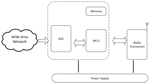
Throughout the recent years wireless technologies have been the focus of investment in telecommunication area which result in a great evolution of them, emphasizing nowadays the fact that almost every intelligent sensor system requires a permanent connection with the user and if one of the main characteristic is mobility for sure it must be wireless in figure 2.7 from [9]. As said before the wireless communications are extremely important when mobility matters, which as well will reduce the number of cables, this section has the purpose to explain the principal wireless protocols.
Memory
Power Supply
Wide Area
Network ADC MCU
Radio Transceiver
CHAPTER 2. UWB COMMUNICATION AND INTERNET OF THINGS
2.3.1 Bluetooth- IEE 802.15.1
The protocol Bluetooth (IEE 802.15.1 standard) is basically a radio system wireless designed for short distances and low-costs devices with the intention of replacing cables of computer peripherals, by this it is possible to conclude it belongs to WPAN. There are two types of connectivity topologies, the piconet and the scatternet. In the first one, the device work as a master which is connected with several devices, working as slaves. The scatternet is a group of different Bluetooth devices overlapping in time and space. Bluetooth operates in the unlicensed 2.4GHz at a rate of 1Mbps [10].
2.3.2 Zigbee- IEE 802.15.4
This protocol, the Zigbee (IEE 802.15.4), working in the same scale of Bluetooth by this means, Wireless Personal Area Network, up to 10m. Zigbee provides self-organized, multi-hop and a reliable mesh networking with a long battery lifetime. Another advantage, it permits low-data rate wireless networking standards that can eliminate the costly and damage prone wiring in industrial control applications. It supports star and peer to peer technologies, Bluetooth is able to operate in the frequency band of 2.4 GHz with a rate of 250 Kbps [11].
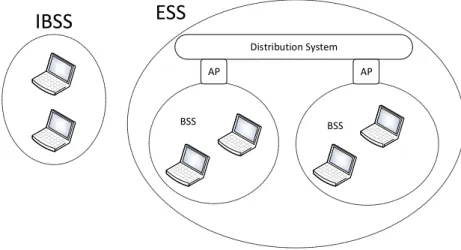
2.3.3 Wi-Fi- IEE 802.15
One of the most well-known protocols in wireless technologies IEE 802.11 (Wireless Fidelity), this protocol belongs to Wireless Local Area (WLAN). All users are able to surf in the internet at great transmission velocities when connected to an access point or an ad-hoc node. The architecture of this system is based in a basic cell which is called basic service set, which is a collection of mobile or fixed stations. For any particular reason, If one of that stations moves from the basic service set (BSS), it will no longer belongs to the same BSS and as a consequence it will lose the ability to communicate with the members of that BSS. Based in this cell is the IBSS and an extended service set (ESS). Under these circumstances, whenever stations are able to directly communicate without an AP, to it is called an IBSS operation.
A IBSS may also form a component of an extended form of network that is built with a multiple BSS. The component responsible to interconnect as a BSS is the distributable
2.3. WIRELESS COMMUNICATION PROTOCOLS
system (DS). Having a DS as APs, it is possible to create a Wi-Fi network ESS in figure 2.8, referred from [12].
Distribution System
ESS
IBSS
AP AP
BSS BSS
Figure 2.8: IBSS and ESS configurations of Wi-Fi networks.
2.3.4 Comparison of Technologies
Standard Bluetooth UWB ZigBee Wi-Fi
IEE spec 802.15.1 802.15.3a 802.15.4 802.11a/f/g
Frequency band 2.4GHz 3.1−106GHz 915MHz; 2.4GHz 2.4GHz; 5GHz
Max signal rate 1Mb/s 110Mb/s 250Kb/s 54Mb/s
Nominal range 10m 10m 10−100m 100m
Nominal TX Power 0−10dBm −41.3dBm/MHz 10−100dBm 15−20dBm
Number of RF channels 79 (1−15) 1/10; 16 14(2.4GHz)
Channel bandwidth 1MHz 500MHz−7.5GHz 0.3/0.6MHz 22MHz
Modulation type GFSK BPSK, QPSK BPSK (+ ASK),O-QPSK
BPSK, QPSK, COFDM, CCK,
M-QAM
Spreading FHSS DS-UWB,
MB-OFDM DSSS DSSS, CCK, OFDM
Coexistence mechanism freq. hopingAdaptive freq. hopingAdaptive freq. selectionDynamic
Dynamic freq. selection, transmit power control
Basic cell Piconet Piconet Star BSS
Extension of the basic cell Scatternet Peer-to-peer clsuter tree, Mesh ESS
Max number of cell nodes 8 8 >65000 2007
Encryption Eo stream cipher (CTR, counter mode)AES block cipher (CTR, counter mode)AES block cipher
RC4 stream cypher (WEP), AES block sipher
Authentication Shared secret CBC-MAC(CCM) CBC-MAC(CCM) WPA2(802.11i)
Data protection 16-bit CRC 32-bit CRC 16-bit CRC 32-bit CRC
CHAPTER 2. UWB COMMUNICATION AND INTERNET OF THINGS
Looking closely to the last comparative table 2.1, adapted from [9] and having into account only the transmission rate of UWB and Wi-Fi technologies are by far the ones who got the best results. It is important to have a look in the spread spectrum techniques particularly in 2.4 GHz where Bluetooth, Zigbee and Wi-Fi coexist, which is an unlicensed band in most countries and known as industrial, scientific and medical band (ISM). Could exist some issues, specially when talking about the band of 2.4GHz, as said before. To help that Bluetooth protocol use an adaptive frequency to make possible to avoid collisions among other channels. Meanwhile Zigbee and Wi-Fi protocols use a dynamic selection of frequency and some power control.
It is also important to refer that the number of cell nodes of the network of Bluetooth are 8, Zigbee star network are over 65000 and 2007 for a structured network Wi-FI [9].
Talking about the transmission time, in [9], it should be referred that it depends on the data rate, message size and distance between two nodes. The formula of transmission time in equation 2.1 is given by,
Tx = (Ndata+ (
Ndata
NmaxPld ∗
Novhd))Tbit+Trpop, (2.1)
whereNdatais equal to the data size,NmaxPldis the maximum payload size,Novhd is
the over head size,Tbit is related to the bit time whileTprop refers to the propagation time
between two devices. Looking to table 2.2 we conclude that Zigbee has the lower data rate and UWB presents the best results when talking about data rate. Data Coding Efficiency, it refers to the ratio of data size with the message size (total number of bytes used to transmit data).
Standard Bluetooth UWB ZigBee Wi-Fi
IEE Spec. 802.15.1 802.15.3 802.15.4 802.11a/b/g Max data rate(Mbit/s) 0.72 110 0.25 54
Bit Time(u s) 1.39 0.009 4 0.0185 Max data payload (bytes) 339 (DH5) 2044 102 2312
Max overhead (bytes) 158/8 42 31 58 Coding effciency 94.41 97.94 75.52 97.18
Table 2.2: Typical system parameters of the wireless protocols.
For small data size bluetooth presents the most favourable results, also noticing that Zigbee also has a good efficiency for this values of data size. When the core issue is big data sizes, UWB and Wi-FI has good results, shown in figure 2.2, based in [13]. Regarding the power consumption, in figure 2.3 it is possible to conclude that the bluetooth and Zigbee Technologies are quite good in Low Data Rate applications [13], as an example
2.4. ULTRA-WIDEBAND
Protocols Transmitted Power (Watt)
Bluetooth 0.1
UWB 0.064
ZigBee 0.0063
Wi-Fi 1
Table 2.3: Transmitted power parameter of the wireless protocols.
limited power batteries. On the other side for High Data Rate, the UWB and Wi-Fi are the best solutions.
2.4
Ultra-Wideband
The Ultra Wideband technology has as main characteristic the transmission of short pulses with low energy, with a fractional bandwidth bigger than 20 % or a signal band-width bigger than 500 MHz. Taking into account Shannon’s capacity formula, this amount of bandwidth offers a high capacity. The UWB transmitter produces a very short time-domain pulse which is able to propagate without the need for an additional radio fre-quency mixing stage. Saying in another words is a carrier-less radio technology which results in a much simpler and consequently cheaper compared to other radio frequency carrier systems. Mentioning as well that in this project an impulse radio UWB transceiver is used.
As said before UWB systems always had some disadvantages however all changed during the past years. In 2002 the Federal Communication Commissions recognised the significance of UWB technology and initiated the regulatory review process of the technology to make it possible to use it for commercial applications, there were a series of factors that by somehow had changed the opinion about impulse radio techniques, mainly:
• The radio frequency (radio frequency (RF)) spectrum is intensively used, making it difficult to get usable broad bandwidth;
• The need for ultra low-power RF communication links which have to be robust in
harsh environments;
• Since the widespread of GPS it become important as well to adopt that to indoor
environments;
CHAPTER 2. UWB COMMUNICATION AND INTERNET OF THINGS P o w er S p ec tr u m D en si ty Frequency Conventional radio signals UWB radio signals
Figure 2.9: UWB Conventional.
In figure 2.9 based in [14] is the comparison of UWB and other conventional radio sig-nals. It should not be forgotten that because of the enormous bandwidth of IR transceivers makes them more resistant to fading effects in severe environments and has a fine time resolution which makes it a technology appropriate for accurate ranging and since it has an enormous bandwidth, it has a good material penetration capability.
As said before, from [8], the signal is recognized as UWB if it has a bandwidth of,
BW≥500MHz, (2.2)
Also according to the federal communications comission (FCC) UWB rulings, a signal can be classified as an UWB signal if the fractional bandwidth (Bf) is greater than 0.2 and
is determined by,
Bf = ( fH− fL
fH+ fL)/2
. (2.3)
Also worth referring that by the Hartley-Shannon theorem,
C=B·log2(1+SNR), (2.4)
whereC is the maximum capacity of the channel, Bis the bandwidth and SNR is
the relation between noise and signal. After giving a close look to this last expression it is possible to refer that the maximum capacity of the channel rises directly with the bandwidth and it is only affected logarithmic with the relation Noise-Signal, knowing that UWB bandwidth has values of frequency around 109, permits to obtain a channel capacity
bigger and larger even working with a relatively low SNR, [15].
2.5. UWB MODULATION METHODS
2.5
UWB Modulation Methods
A fundamental part is the modulation of the signal to send where the designer has a wide range of options. However exists a trade-off in UWB Modulation systems, this is related to the maximum transmit distance, the data rate, the transmission power and system complexity. The main data modulation schemes are PPM, PAM, PSK and OOK.
2.5.1 PAM
The basic principle for this modulation, figure 2.10 relies in sending the signal with different amplitudes corresponding to different data being transmitted and expressed by equation 2.5, from [16].
Figure 2.10: PAM modulation.
s(t) =
∞
∑
m=1
bm∗P(t−mT)) (2.5)
This type of modulation presents low complexity once it just requires a single polarity to represent data and it depends on an energy detector to recover data, on the other hand, PAM is sensitive to noise and attenuation which can make 1 and 0 hard to distinguish.
2.5.2 OOK
Figure 2.11: OOK modulation.
CHAPTER 2. UWB COMMUNICATION AND INTERNET OF THINGS
while its absence represent bit 0 as showed in figure 2.11 and represented by equation 2.6, from [16].
s(t) =
∞
∑
m=1
bm∗P(t−mT)), (2.6)
represented asP(t)is an extremely narrow pulse,bmrefers to the bit information and
Tis the pulse period. This modulation was used in this project since it represents low
complexity either in the modulation or in the demodulation however it is important to emphasize that this type of modulation has some drawbacks like being too sensible to noise and to interferences, causing a BER performance below the expectations.
2.5.3 PPM
Figure 2.12: PPM modulation.
The PPM modulation, figure 2.12, [16], is based on the determination of the UWB pulse position, it is necessary to predefine a time window where the 1 bit can be represented by the original pulse and bit 0 by the translated pulse in time.
s(t) =
∞
∑
m=1
P(t−mT−bmδ)), (2.7)
in equation 2.7, [16],P(t)is an extremely narrow pulse,bmrepresents the bit information
andTis the pulse period andδis a time delay, in this modulation the noise is significantly
lower compared with the techniques mentioned before, however it comes with a price, it is vulnerable to collisions caused by multi-access channels and they are also much more complex to implement.
2.6. UWB REGULATIONS
Figure 2.13: BPM modulation.
2.5.4 BPM
In the BPM modulation, [16], as shown in figure 2.13 to represent the information bits the pulse polarity is switched, in other words bit 1 has a positive polarity and bit 0 has a negative polarity.
s(t) =
∞
∑
m=1
bm∗P(t−mT±δ) (2.8)
As main advantage, it is less susceptible to distortion because the signal is detected by the polarity and just by looking to equation 2.8, demonstrated in [16], represents a higher complexity than in the first two techniques.
2.6
UWB Regulations
In order to minimize the interferences from UWB in other technologies, since it radiates electromagnetic energy in a large spectral band, the limits of maximum radiation level and the frequency bands of free licensed operation from UWB devices have as expected certain regulations that must be fulfilled, [17].
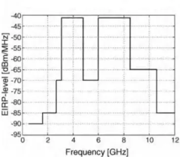
CHAPTER 2. UWB COMMUNICATION AND INTERNET OF THINGS
The first regulation came from USA, introduced by the FCC as it is possible to see in figure 2.14 from [1], permitting a working frequency band between 3.1 to 10.6GHz for UWB radiation with a limit of power around -40dBm/MHz. To fit it for Europe utilization was necessary to modify these rules, which is a bit more restricted showed in figure 2.15, [1], comparing it with United state regulations. One of the main areas is the communication industry, the biggest supporter of UWB regulation, and it is expected an enormous market for high-data-rate in short range communication. It is important to refer that exists many different masks depending on the utilization for example for indoor and outdoor utilizations should be different, [17].
Figure 2.15: FCC-Europe.
2.7
Gaussian Pulse
It is truly important to maximize the radiated energy of the pulse, as long the spectral FCC mask is respected. In the UWB signal the spectrum in frequency domain depends on the waveform of the used pulse, where the main ones are rectangular, Gaussian doublet and mono-cycles. To satisfy the UWB emission constraint specified in FCC regulation the desired frequency spectrum of the mono-cycle wave form should be flat over a target bandwidth, [18]. Having as expression,
V(t,fc,A) = A·e−2(πt fc)
2
. (2.9)
2.7. GAUSSIAN PULSE
10 20 30 40 50 60
0 0.2 0.4 0.6 0.8 1 Samples Amplitude Time domain
0 0.2 0.4 0.6 0.8
−80 −60 −40 −20 0 20 40
Normalized Frequency (×π rad/sample)
Magnitude (dB)
Frequency domain
Figure 2.16: Gaussian pulse and frequency spectrum.
−5 −4 −3 −2 −1 0 1 2 3 4 5 x 10⁻⁵
−0.8 −0.6 −0.4 −0.2 0 0.2 0.4 0.6 0.8 1 time (s) Voltage (V)
Figure 2.17: gaussian monocycle pulse.
In equation 2.9, where the value ofAis the amplitude of the pulse and fcis the centre
frequency. In order to obtain the derivative of equation 2.9 it was used Matlab to simulate a gaussian pulse and to calculate it frequency spectrum, shown in figure 2.16.
V(t, fc,A) =2√e·A·πt fc·e−2(πt fc)
2
, (2.10)
equation 2.10 represents the gaussian monocycle pulse which is represented in fig-ure 2.17. The central frequency is defined as(πτ0)−1, whereτ0 is the time between the
CHAPTER 2. UWB COMMUNICATION AND INTERNET OF THINGS
2.8
UWB Transceivers
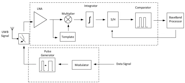
As everything in the area of technology has a trade-off, there are a vast number of topolo-gies for the same purpose and this happens as well in UWB circuits. Focusing in the Low Data Rate transmission is shown in this chapter that exists three main topologies Differential Coherent System topology, Coherent System topology and giving special attention to the Non-Coherent system topology, which will be implemented in this project.
2.8.1 Coherent Systems
BaseBand Processor Rx Data Sync Data Clock Generator Syncronizer UWB Signal Pulse Generator VCO Buffer LNA Multiplier VGA Comparator Temp Buffer
Figure 2.18: Coherent System.
From the different UWB systems available, the one with better results up to this date is the coherent, it presents a superior BER outcome with long range. However it is a complex architecture and as a result bigger current consumptions, this issue happens because it is necessary to estimate the channel with high precision and an almost perfect synchronization with each correlator. In figure 2.18, [19], illustrates the overall architecture of a coherent IR-UWB transceiver.
In the transmitter, the data signal from baseband is the input of the digital pulse generator which converts in short pulses. The short pulse makes the LC voltage-controlled oscillator (VCO) turn ON/OFF, and finally the modulated UWB pulse is transmitted through the differential buffer amplifier and to the antenna. While in the receiver, the UWB signal is amplified at the low noise amplifier (LNA) stage, the amplified signal is demodulated with the template signal in the multiplier. Therefore the demodulated pulse envelope signal is filtered by the following low pass filter, and is amplified adaptively in the VGA stage to achieve the sufficiently dynamic range. Finally, the comparator makes
2.8. UWB TRANSCEIVERS
the digital output pulse data whenever the magnitude of signal exceeds the controllable threshold voltage level.
2.8.2 Differential Coherent Systems
BaseBand Processor
UWB Signal
Modulator Pulse
Generator LNA
Multiplier
Comparator
S/H
Template
Integrator
Data Signal
Figure 2.19: Differential Coherent System.
The second transceiver system shown in figure 2.19, [19], uses a modulation scheme of transmitted reference also known as Differential coherent. Where a transmitted reference communications system transmits two versions of a wideband carrier, one modulated by data and the other unmodulated. Typically both, modulated and unmodulated versions are separated from one another either in time or in frequency.
C
H
A
P
T
E
R
3
D
ESIGN OF THE PROPOSED
UWB
TRANSCEIVER
This chapter introduces the proposed UWB transceiver, considering the information given in the previous chapter where alternatives for non-coherent transceiver were anal-ysed.
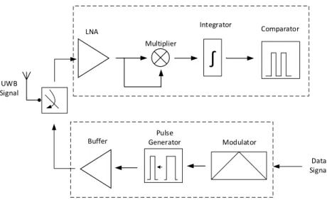
One of the first choices to make is to determine which modulation type presents the best robustness and flexibility results, for a proper wireless connection. To achieve all these characteristics exists the Non-Coherent transceivers, based in [20], characterised for having a low cost and low energy consumption once it does not need to do an estimation of the transmitted channel. However as main disadvantages it has low performance of BER, once the signal is detected through it energy, as a result comparing with other techniques it turns to be really sensible to noise, to interferences and to multipath effects.
3.1
Transceiver Architecture
CHAPTER 3. DESIGN OF THE PROPOSED UWB TRANSCEIVER
LNA
Multiplier
Comparator
Integrator
Pulse Generator
Buffer Modulator
UWB Signal
Data Signal
Figure 3.1: UWB Non-coherent transceiver.
3.2
Transmitter
3.2.1 Modulator, Pulse Generator and Driver Amplifier
The transmitter is composed by a modulator, a pulse generator and a driver amplifier. For the design of an UWB system is crucial to select the modulation type, since it will have a direct impact in the transceiver complexity, the data rate, bit error rate (BER) and robustness against interferences, [21]. For this thesis the ON/OFF keying modulation is the most appropriate once it is the one that best fulfill the demands of IoT systems. The block scheme of the OOK modulation, is shown in figure 3.2
Clk
Data
NAND
Figure 3.2: ON OFF Keying modulation.
After having the signal modulated it will be generated a short pulse in which will be sent through the antenna, creating a gaussian pulse. Therefore, the modulated signal will be sent to the input of the pulse generator, figure 3.3, in which every time the data goes low appears a positive pulse at the output, figure 3.3, where it exists a delay carried out by the inverter chain as a result only in case of having both inputs with low value, 0, that will result in a pulse, having a width determined by the inverters gain delay.
In figure 3.4 is shown a simplification of the waveforms expected through transmitter signal path [22], starting from the data that is meant to be sent, the clock of the transmitter that will determine the number of pulses to be sent, the signal modulated with a OOK modulation technique and, the last one, is the signal after the pulse generator.
3.2. TRANSMITTER
Modulated Signal
NOR Inverter
Chain
Vpulse
Figure 3.3: Scheme of Pulse Generator.
Time
Data
signal
Clock
Modulated
signal
Generated
pulse
Figure 3.4: Signal waveforms through different blocks of the transmitter.
The driver amplifier is the last circuit of the transmitter just before the antenna which it is used to amplify and shape the modulated pulse signal into regulated spectrum mask and it is responsible for the matching the block with the dipole antenna.
One of the most basic topologies of a wideband power amplifier is the Class A RF, in figure 3.5 from [23], it is based in a single transistor with a parallel-resonant circuit LC, a RF chokeLf and a coupling capacitor Le, which will have as operating point the active
region and the transistorM1works as a voltage-controlled dependent current source. For
this case a wideband characteristic is expected, there is no need of filters.
Once the class A has the highest conduction angle of all linear amplifiers it results in a lower efficiency around 25%, it can be written as,
ηD = Pout
PDC
= 1 2 ·(
Vout
VDC
)2. (3.1)
WhereVoutis the output voltage value. Concluding, 50% of efficiency is the maximum
CHAPTER 3. DESIGN OF THE PROPOSED UWB TRANSCEIVER
VIN
VDD
L
M1
Vou t
R
Figure 3.5: Signal waveforms through different blocks of the transmitter.
3.2.2 Antenna
As it is said by definition an antenna is meant for "radiating or receiving radio waves", [24]. It converts signals from a transmission line to electromagnetic waves to broadcast it and in the receiver antenna converts back into electrical signals.
There are some parameters that should be taken into account to elect the most ap-propriate antenna, including directivity, gain, input impedance, frequency pattern and antenna size.
Frequency Bandwidth
Frequency Bandwidth is the parameter that represents the range of frequencies.
As mentioned before a wideband system has an antenna characterised for having an absolute bandwidth value (ABW) greater than 500 MHz or a fractional bandwidth (FBW) greater than 20 %.
Radiation Pattern
Radiation Pattern describes as the name indicates the representation of the radiation properties of the antenna, normally the pattern characterises the power levels.
Directivity and Gain
From figure 3.6, [24], is the description of a generic antenna where Rr, RC, L and C
represents the radiation resistance, loss resistance, inductor and capacitor, respectively.
3.2. TRANSMITTER
Rs
CA
C L
RC Rr
Figure 3.6: Generic electric circuit of an antenna.
Looking to [25], the radiation efficiency can be described by,
erad= Rr
Rr+RC
. (3.2)
The maximum gainGo is directly related to radiation efficiency and maximum
direc-tivityDoin,
Go = erad·Do. (3.3)
UWB antennas should have as main characteristic an absolute bandwidth no less than 500MHzor a fractional bandwidth at least 20%. UWB antennas requires a consistent be-haviour over the entire operational bandwidth, it should be directional or omnidirectional depending on their functionality, another important feature is it scale once it will have an application in mobile phones or in any other small devices and the UWB antenna should have a good time domain performance with minimum pulse distortion in the received waveform.
The most common on-chip antennas in UWB systems are the dipole antennas, monopole antennas and loop antennas.
Loop Antennas
Loop antennas, as the name indicates these type of antennas are characterised for having a single rounded element.
CHAPTER 3. DESIGN OF THE PROPOSED UWB TRANSCEIVER
In figure 3.7, based in [26], shows a loop antenna which leads to a considerable area occupied, however it is compensated with an higher gain.
Monopole Antennas
These antennas are the simplest topology, it is based in a single element fixed on ground plane. With this characteristic the ground plane become a mirror image of the element above the ground, which will act as it was a dipole antenna figure 3.8 based in [26].
λ
/4
Ground
Figure 3.8: Simplified scheme of monopole antenna.
Having half of the length of a dipoleλ/4, and an inferior performance compared with
the other topologies, to better describe the it there is the expression of the gain from [25] and expressed by,
G=4·πAe
λ , (3.4)
whereλis the wavelength and Aeis the aperture area of the antenna.
Dipole Antennas
Pulse Generator
λ/2
Figure 3.9: Simplified scheme of dipole antenna.
3.3. RECEIVER
Looking to the available antennas and having in consideration all the trade-offs, for example the size, the complexity and power consumption the chosen one was the electric dipole antenna, a simple diagram is shown figure 3.9, [26].
3.3
Receiver
The receiver of the proposed non-coherent IR-UWB system, looking to figure 3.1 is charac-terised for having a large gain and low noise figure (NF) LNA, in order to achieve this features a great effort was needed to make. Once as referred before it presents an absolute bandwidth of 500MHzwith a centre frequency of 4.5GHzturning it in a great challenge to
obtain a good performance. This block will contribute for a lower noise contribution from the next stage, making a lower NF receiver and resulting in higher sensitivity and data rate, which are crucial characteristics. The next wideband IF blocks consist in a squarer, an amplifier and at the end a 1 bit ADC, which it is based in a comparator, implemented with a simple differential pair and a regenerated latch.
3.3.1 Low Noise Amplifier
The first circuit of the IR-UWB receiver is the Low Noise Amplifier (LNA). To achieve these goals it is essential that the input impedance matches the antenna characteristic impedance in order to maximize the power transfer. It is important to note that in the LNA circuit should be achieved the minimum noise as possible in the system and naturally having in consideration the gain and the Noise Ratio.
One of the main requirements to choose a proper topology for this IR-UWB system, it must have an high bandwidth and the input impedance needs to match the antenna impedance for the LNA Working band, for these desirable requirements exists several topologies however for a high frequency of work, around 4.5GHz, there are few with
the simplicity and efficiency of the Wideband Cascode Balun-LNA which is based in two simple topologies the Common Gate and the common source.
The Common Source is a strong candidate for a Low Noise Amplifier figure 3.10 from [27], once it is one of the simplest way to match the input, usingRI Nas a resistance that
will provide a more stable input through the working band of the LNA. However as a simple amplifier it turns to have a considerable value of Noise Factor.
It should be mentioned as well, that resistance is in parallel with the gate of the transistor, it is important to refer the motive for the use of this resistor since the input impedance transistor is infinite one of the ways to match it is with a resistor in parallel andZLimpedance represents a wideband configuration.
Nevertheless, it is essential to refer that the resistor introduces a significant quantity of noise to the overall system. As a result the expression of the Noise Factor of the entire Common Source, there is in equation 3.5, withGAas the power gain available, the Noise
CHAPTER 3. DESIGN OF THE PROPOSED UWB TRANSCEIVER
c
VDD
ZL
RIN
ZIN
Figure 3.10: Common Source LNA.
looking close to the next equation we can conclude that the minimum value of noise is 2
dB, which only ideally can be achieved, with this simple LNA, demonstrated in [27] and
expressed by,
F= 4KTRSGA+4KTRI NGA+PN 4KTRSGA
=2+ PN 4KTRI NGA
(3.5)
Another possibility for the LNA is the Common Gate LNA, is shown in figure 3.11 based in [27], at it simplest form, it is the topology more used in the wideband LNA, this happens because it presents an intrinsic wideband response. In order to achieve a 50Ω
(antenna impedance), the transconductance gain,gm, of the common gate will need to be
equal togm = R1S =20ms, this only can be verified if the channel length modulation and
body effect are ignored.
VBIAS
VDD
ZL
ZIN
Figure 3.11: Common Gate LNA.
Referring only to thermal noise [22] , whereNoandNiare the power noise at the input
3.3. RECEIVER
and output of the LNA, the minimum noise factor can be easily obtained,
F = No NiGA
(3.6)
Having Ni = IS2andNo = (IS2+Id2)G˙A
F= (I
2
S+Id2)GA
IS2GA
=1+ I
2 d
IS2 (3.7)
Knowing that IS2 = 4KTγgmfrom [22] as well as Id2 = 4KTgm, which is the medium
value for the thermal noise. The Noise Figure is given by,
F=1+4KTγgm
4KTgm =1+γ, (3.8)
Considering the use of long channel transistors, the constantγhas a value of 2/3, while
the minimum value of noise factor from a common gate amplifier is equal to 5/3, around 2.2 in dB which is lower than the common source topology. One of the main disadvantages is the need of resizing thegm in order to match the input impedance, so it is mandatory to
increaseZL, once it is directly proportional with the gain of the amplifier which results in
a higher NF, normally greater than 3 dB. In order to overcome this values of Noise Factor a possibility is by somehow combine both topologies using a noise cancellation principle.
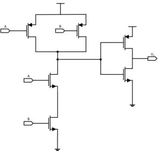
3.3.2 Self Mixer
In the RF front-end systems, specially in a non-coherent where it has a goal of being as simple as possible results in the necessity of a self-mixer, the block responsible for the square of the signal resulting in translation of the frequency RF signal to an Intermediate frequency, called up-conversion or the opposite down-conversion since it transfers the frequency to the baseband. In an ideal world it is a simple calculus, just a multiplication. However different frequencies are expected from the sum and difference of the two signals that are in the two inputs, showed in figure 3.12. From the different mixer topologies it was decided for a active mixer, in figure 3.13.
)
sin(f t
VRF RF 2 sin(( ))
1 )
sin(f t V V f f t
VIF IF RF RF RF RF
)
sin(f t
VRF RF
Figure 3.12: Self Mixer frequency sum.
CHAPTER 3. DESIGN OF THE PROPOSED UWB TRANSCEIVER
expected output is:
VRF =1/2VLOVIFcos((fIF+ fLO)t). (3.9)
And as a real component it has a gain, based in the division of two inputsIFandLO,
equal to,
A=20·log(VLOVIF VIF
) =20log(VLO
2 ). (3.10)
As it was said before the mixer is a non-linear system. As a consequence it will appear other unwanted frequencies, which subsequently results in a different value of the final gain which can be lower or higher.
A=20log(VLOA
2 ) (3.11)
So the conversion gain, in equation 3.11 with all the undesired frequencies summed up asA, demonstrating how efficient the global mixer is, if the mixer has value of conversion
gain greater than 1 dB it is considered active otherwise a passive mixer. The mixer will have it noise energy lower or higher than the translated signal. In other words, every noise from sources will be translated and replicated however it has the benefit of being wideband which result in an aliasing effect. For the self-mixing process of the receiving signal it is used a wideband Gilbert Cell which is based in the single balanced mixer , therefore having a close look to the single balanced mixer which is an active topology it has the purpose of multiplying the signals in the current domain.
VRF VLO
VDD
M1 M2
M3
RD RD
Figure 3.13: Single Balanced Mixer.
Looking to figure 3.13, it is possible to notice that the single balanced mixer is based on a simple differential pair and since one of the easiest ways to obtain the desired mixing
3.3. RECEIVER
is with a switch. It works basically by using a differential pair, by this it is meant that the pair commutes the current flow between it branches, a switching behaviour is acquired and a mixing effect can be achieved.
A switching behaviour is achieved when a large signal, that represents the input of the mixer,M1andM2are in the saturation region, which means that when the switch is
closed the impedance is low on the other hand when opened the impedance is infinite, in the transistor can work as a current buffer relatively to the current signal injected.
With all these conditions, the transistor’s bias point vary with the same period in time and the current that flows in each branch depends on the differential voltage as well as in the bias current (ISS). Knowing that in figure 3.13,VD is the differential input voltage,
with a phase shift of 180, IB1,2 is the drain current and vOD is the differential voltage.
Considering both transistors with the same size and neglecting body effect, the output currents are given by,
IB1 =K·(Vgs1−Vth1)2 (3.12)
IB2 =K·(Vgs2−Vth2)
2 (3.13)
Considering as well ideal current sources,
VD = (Vgs1−Vgs2) =
r
ID1 k −
r
ID2
k (3.14)
with,
ISS= IB2+IB1 (3.15)
which means that,
IB2 = IB1 = ISS
2 + √
k−vD· r
ISS
2 −
k
4v˙2D (3.16)
Havingkas the mobility constant in the DC point, which is equal to:
k= ISS 2(VGS−VTH)2
(3.17)
ID1 = ISS
2 +
ISS
2 ·
vD
(VVGS−VT)2 s
1− 1 4·(
vD
VGS−VT
)2 (3.18)
Looking to the small signal of one common source is obtained the gain of the dif-ferential pair, in equation 3.19 since the outputs are in phase opposition, we have in equation 3.20.
voD =vo1−vo2= v1·gmRD+v2·gmRD =−gmRD(v1−v2) (3.19)
CHAPTER 3. DESIGN OF THE PROPOSED UWB TRANSCEIVER
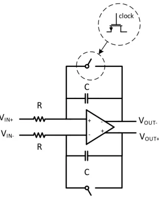
3.3.3 Integrator
The third block of the receiver, dimensioned in this thesis, is an integrator responsible for enhancing the signal strength of the receiving chain, where based in an energy detector working as an accumulator of pulses in order to obtain the exact quantity for bit 1 and 0. So in order to get a better SNR value it is implemented an amplifier buffer in a fully differential integrator topology where the reset of integration (accumulation of pulses) is completed by a CMOS transistor working as a switch, which will turn on in 10 pulses received in other words with a periodicity of figure 3.14. Ideally the transfer function of an integrator is given by,
H(s) = 1
sC. (3.21)
WhereCis the value for the capacitance of each differential mesh.
V
IN+V
IN-R
R
C
C
V
OUT-V
OUT+clock
+
-+
Figure 3.14: Differential integrator.
In order to achieve low power consumption with low voltage it is used a rail-to-rail input/output operational amplifier. As it is expected, the amplifier is designed to work with a big input common mode voltage (Vicm) range, which will maximize the SNR value
of the amplifier, it is important to take a close look to the bandwidth, the phase margin, gain, power consumption.
3.3. RECEIVER
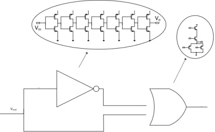
3.3.4 Comparator and Latch
The last part of the transceiver system is divided in two circuits, the comparator and the NAND SR Latch, [29].
The comparator is used to detect a energy signal, by simply using as inputs the data signal and a reference voltage, if the data signal voltage is higher than the threshold voltage it will lead to a high value, "1". It is responsible for the demodulation of the received signal (ADC), one of the main characteristics that the block should have is a high speed response with low power in the minimum area possible. These features are not easy to achieve once the available supply voltage is relatively low, which result in the need of larger transistors subsequently more die area and power needed, so that the requirements will be granted. The comparator is based in a strong-arm latch which is used because of it high sensitivity and low circuit complexity, it is also important to refer that it consumes zero static power, directly produces rail-to-rail output swing and as well high input impedance.
The SR NAND Latch is used in order, in the output of the comparator, to obtain the final output equivalent to the data that was meant to be sent.
The SR NAND Latch, in figure 3.15, is used after the comparator to provide a system output equivalent to the data that is meant to be sent. The latch is one of the simplest circuits of memory elements. It is based in two cross-coupled logic inverters, these logic elements arrange a positive feedback loop, having a number of two stable operating points, the low value is "0" and the high value is "1".
NAND
NAND
S
R
Q
Q
Figure 3.15: SR NAND Latch.
For the UWB system presented in this thesis and in order to trigger the states of the latch it is used the SR flip flop type, in particular using as a latch two NAND logic gates, in cross-couple connection. It is widely known that the two inputs are considered as S (set) and R (reset). The outputs areQ, for low value andQfor high value. When the user does not want to change the state, memory state, the two inputs must be high. It is necessary to refer that if bothS and Rare changed to 0 at the same moment, both NAND gates
CHAPTER 3. DESIGN OF THE PROPOSED UWB TRANSCEIVER
Table 3.1: SR NAND Latch truth table
R S Qn+1
0 0 Q_n
0 1 1 1 0 0 1 1
C
H
A
P
T
E
R
4
E
LECTRICAL
S
IMULATIONS OF THE
P
ROPOSED
T
RANSCEIVER
This chapter introduces the electrical simulations of the proposed IR-UWB transceiver, shown in figure 4.1. The transceiver has been described in a CMOS 130 nm technology.
LNA
Multiplier
Comparator
Integrator Modulator
UWB Signal Pulse
Generator Buffer
UWB Signal Data
Signal
Figure 4.1: Complete transceiver architecture.
4.1
Transmitter
4.1.1 Modulator and Pulse Generator
CHAPTER 4. ELECTRICAL SIMULATIONS OF THE PROPOSED TRANSCEIVER
B
Vo
A
A B
Figure 4.2: NAND logic gate.
Table 4.1: Truth table of NAND logic gate.
A B S 0 0 1 0 1 1 1 0 1 1 1 0
The signal modulator OOK designed, is a simple NAND logic gate, in table 4.1 there is the logic table for the NAND and in figure 4.2 from [31] , whenever exists a control signal the NAND will produce the same pulse with a frequency equal to the clock rate signal.
Once the digital sequence that represents the analog signal is defined the pulse genera-tor block is designed, in figure 4.3 that will represent the bit sequence and once introduced in the antenna they will origin UWB pulses, [32]. The pulses are the result of delays made by logic operations that constitute the generator. The signal once introduced in the generator input it is submitted to a chain of inverters to perform a delay in the signal, to be worked in the NOR, in table 4.2 is the truth logic table of a NOR, with the original signal as well. Varying the value of the delay , it is possible to create pulses with higher or lower period which will be reflected later in the bandwidth occupied by the Gaussian pulses.
Table 4.2: Truth table of NOR logic gate.
A B S 0 0 0 0 1 0 1 0 0 1 1 1
When there is two low signals at the inputs of the NOR logic gate it will produce a logic
4.1. TRANSMITTER
Vmod
Vmod
Vpulse
Vo
Vin
B A
A B Vo
Figure 4.3: Pulse generator.
pulse. The length of the pulse is defined by the period of time in which both input signals are at low state, as mentioned before is programmed by the delay chain of inverters.
Simulation
In order to prove the veracity of the blocks responsible for modulation and pulse gen-eration they were simulated having a supply voltage ofVDD =1.2V, transistors with a
minimum length and maximum width to guarantee a quick response, permitted by the 130nmCMOS technology which is 120nmfor theLand aW of 115.2µm
In figure 4.4 is shown waveforms of the two first blocks of the transmitter, the first signal is the the data meant to be sent, the second one is the modulated signal, with OOK modulation using a NAND port logic as said before and using a clock signal with 10KHz
that will work as carrier. The last is the pulse already generated with a signal period of 4
CHAPTER 4. ELECTRICAL SIMULATIONS OF THE PROPOSED TRANSCEIVER
196 198 200 202 204 206 208 210 212 214 216
−2 0 2
time [ns]
Vc
k
[V]
196 198 200 202 204 206 208 210 212 214 216
−2 0 2
time [ns]
Vd
at
a
[V]
196 198 200 202 204 206 208 210 212 214 216
−2 0 2
time [ns]
Vm
o
d
u
lat
ed
[V]
196 198 200 202 204 206 208 210 212 214 216
−2 0 2
time [ns]
Vp
u
ls
e
[V]
Figure 4.4: Modulator and Pulse Generator.
4.1.2 Driver Amplifier
The driver amplifier, [30], has the role of driving the signal to an antenna with 50Ωof
impedance, this block is constituted by two stages. The first one is composed by a common source cascode and a common gate with inductive degeneration, while the second stage is a source follower, as it is possible to see in figure 4.5. Through the model of small signals the voltage gain is given by:
Av = 1−gmZL
+gmZS
(4.1)
Having the transistor M1 biased in the linear region it means that the current is described by:
iD = µnCoxW
L
(VGS−VT)VDS−
1 2VDS2
(4.2)
Whenever theVDSis significantly small, the second order term will disappear,
conclud-ing we obtain a linear function and we can put in order ofrDS:
4.1. TRANSMITTER
rDS =
1
µnCoxWL(VGS−VT)VDS
(4.3)
The Common gate transistor M2is designed to work as a resistance, which means it
will work in the linear region, that could be controlled by varying the bias voltage from
M2transistor.
Figure 4.5: Driver Amplifier.
The gain of M2 (linear region) obtained by analysing the small signals at high frequency is,
AV = −gm1ZL−gmrDS
+gmZS
(4.4)
substitutingrDSby its expression
AV = −
gmZL−gmµnCoxWL(VGS−VT)VDS
1+gmZS
(4.5)
CHAPTER 4. ELECTRICAL SIMULATIONS OF THE PROPOSED TRANSCEIVER
Table 4.3: Driver Amplifier parameters.
Transistor W(µm) L(µm) Region ID(mA) VDSat(mV) gm(mS)
M1 64 0.12 active 1 83.6 8
M2 64 0.12 active 1 80.7 4
M3 115.2 0.12 active 2 84.6 34.6
10−1 100 101
0 10 20 30 40 50 60 frequency [GHz] Z 22 [oh m ]
Figure 4.6: Output impedance.
Simulation
To verify the Driver amplifier equations that were studied few simulations were made having in consideration the circuit limitations as it was showed before with a supply voltage of 1.2Vtable 4.3 shows the main parameters of the transistors, their dimensions
and DC operating, that form the driver amplifier (DA).
The output impedance is not the ideal value but still good enough to obtain a decent signal, in figure 4.6 is the impedance with a value of 33Ωfor the desired bandwidth.
196 198 200 202 204 206 208 210 212 214 216 218 0 0.1 0.2 0.3 0.4 0.5 0.6 0.7 0.8 0.9 time [ns] V ou t [V]
Figure 4.7: Waveform output of Driver Amplifier.
4.2. ANTENNA
The signal after having the output matched with a value of 50Ωin figure 4.7 it has maximum peak approximately in 1.2Vwith a duration of 5nssince this is the designed
pulse, it is not rectangular.
4.2
Antenna
As for the transmitter antenna as for the receiver antenna, which have the same architecture and values was done the proper design and simulation in the ADS environment where was taken special attention to the spectral power density. As mentioned before dipole antenna is far from perfect, however it has as advantages low consumption and simplicity, which turn it one of the best for UWB signal transmission. To validate this type of antenna it is necessary to match the antenna by knowing previously the desired frequency for transmission, [33]. To design the dipole antenna it was used an electric circuit.
Rs C Cp L Rl Rr CA + -+ -C Cp RL Rr L
Figure 4.8: Dipole antenna.
As shown in figure 4.8, the antenna is described as a circuit with passive elements, [34]. The resonance series composed byC1andL1describes the antenna behaviour,R1is
the resistor that represents the radiation resistance which simulates the antenna radiation. The signal that was chosen to be transmitted has a centre frequency around 4.5 GHz,
all the calculation of the passive elements were made to replicate the behaviour of a dipole antenna ofλ/2 length. To theoretically describe the wavelength of the signal, in
equation 4.6, which consists in the relation between the light speed in vacuum with the signal frequency as it is explained in [35] and showed as,
λ= c
f (4.6)
λ= 300.000.000m.s−
1
4.000.000.000s−1 =0.075m (4.7)
Using equations of the resonant frequency of the antenna and using the quality factor Q.
f0= 2w0
π =
1