i
October, 2018
Manuel Manta Chapa
Licenciado em Ciências de Engenharia de Micro e Nanotecnologia
2D Optimization of Thin Perovskite/Silicon
Four-Terminal Tandem Solar Cells
Dissertação para obtenção do Grau de Mestre em Engenharia de Micro e Nanotecnologias
Orientador: Dr. Manuel J. Mendes, Invited Assistant Professor, FCT UNL
Co-orientadores: Prof. Rodrigo Martins, Full Professor, FCT UNL
Presidente: Júri:
2D Optimization of Thin Perovskite/Silicon Four-Terminal Tandem Solar Cells
2D Optimization of thin perovskite/silicon four-terminal tandem solar cells
Copyright © Manuel Manta Chapa, Faculdade de Ciências e Tecnologia, Universidade Nova de Lisboa.
2D Optimization of Thin Perovskite/Silicon Four-Terminal Tandem Solar Cells
iii
“
If the human brain were so simple that we could understand it, we
would be so simple that we couldn’t.”
2D Optimization of Thin Perovskite/Silicon Four-Terminal Tandem Solar Cells
v
Acknowledgements
Quero começar por agradecer ao meu co-orientador, Prof. Rodrigo Martins e Prof. Elvira Fortunato pelo esforço que certamente foi, e ainda é, necessário para criar um curso pioneiro em Portugal e providenciar a oportunidade única a todos os actuais, passados e futuros alunos de se envolverem numa àrea de vanguarda como a da nanotecnologia. Também são merecidos agradecimentos ao meu orientador, Prof. Manuel Mendes por me introduzir ao mundo da simulação computacional e pelos conselhos dados durante todo este trabalho.
Agradeço ao centro UNINOVA-CEMOP e ao projecto ALTALUZ - PTDC/CTM-ENE/5125/2014 pela oportunidade de integrar num projecto de I&D em fotovoltaicos.
Um grande agradecimento aos meus parceiros de simulação, Fábio Vieira e Miguel “Douradinho” Alexandre pelos dias passados na sala 202 a resolver problemas e a “fritar” os portáteis enquanto chegávamos várias vezes perto da insanidade total. Aproveito também para agradecer ao Mestre Sirazul Haque pelos tutoriais dados e ajuda valiosa em resolver aspectos cruciais deste trabalho.
Obrigado a todos os amigos que tornaram esta jornada de cinco anos mais fácil de passar. À Rita Fragoso pelas alheiras no forno nos dias de teste, ao João Teles por me encontrar os óculos quando é preciso, à minha afilhada não oficial Ana “Péssima” Pinheiro pelas risadas e apoio constante, aos emigrantes João Pina e Miguel Ramos, ao Nuno Lima pelas dúvidas em alturas parvas, horas passadas na Teresa e conversas sem fim, e à Catarina Marques por tornar possível tanta piada sobre colégios de freiras. Aos restantes que, embora não mencionados, também foram muito importantes, deixo o meu sincero agradecimento.
Tenho que agradecer aos meus pais, Adelino e Ana, pela paciência toda nestes vinte e três anos, redobrada ou triplicada nos últimos cinco e por terem sempre um bom conselho preparado. À minha irmã Inês, por todos os ensinamentos óbvios e menos óbvios, e pelas experiências que só nós os dois podiamos criar.
2D Optimization of Thin Perovskite/Silicon Four-Terminal Tandem Solar Cells
vii
Abstract
A model capable of describing the optoelectronic response of tandem photovoltaic cells is introduced, employing commercial software provided by Lumerical Solutions Inc. Specifically, a four-terminal thin perovskite/silicon architecture is studied, with special focus on the optical properties of the interlayer, and also on the ITO contact problematic – tackled by an alternative design, where all but one transparent contact are comprised of state-of-the-art transparent metallic structured grids. Furthermore, a look into how light-trapping formalisms are essential to the suc-cess of this architecture is taken.
Thus, this research aims to demonstrate the means to overcome one of the main constraints in tandem cells performance, the transparent oxide’s parasitic absorption characteristics. Addi-tionally, the possibility of highly efficient, thin and flexible, solar cells is explored, being con-cluded that these can be achieved with the referred architecture after careful optimization of the design parameters. The developed optoelectronic model can predict the response of heterojunc-tion solar cells, and also of modelling perovskite solar cells – aspects which are not commonly reported in recent literature.
The parasitic absorption is reduced by 30% when replacing two ITO contacts by the novel metallic grid alternatives. Simultaneously, on a hypothetical light-management scenario where 10x optical path length in the bottom layer is implemented, up to 27% efficiency is achievable by the tandem device.
The attained results can be used as a guideline for forthcoming architecture improvements showing promise for the future of thin and flexible photovoltaic applications.
viii
Resumo
Neste projecto é introduzido um modelo computacional capaz de simular o comportamento optoeletrónico de fotovoltaicos em configuração tandem, com o recurso ao software comercial da Lumerical Solutions Inc. Em específico, uma arquitetura de quatro terminais perovskite/sílicio é estudada, onde é dado foco às propriedades da interlayer e na problemática dos contactos de ITO. Esta última problemática é enfrentada com um design alternativos, onde todos menos um dos contactos transparentes são compostos por estruturas metálicas transparentes. Também é projectado a performance desta arquitectura quando implementadas soluções de light-trapping.
Desta forma, esta pesquisa almeja demonstrar como ultrapassar uma das principais falhas apontadas à arquitetura tandem, a absorção parasitica dos óxidos transparentes. Mais, explora-se a possibilidade de células fotovoltaicos de alta eficiência e baixa espessura. Capaz de modelar o comportamento de células de perovskite, o modelo optoeletrónico desenvolvido tem também a capacidade de prever a resposta de dispositivos fotovoltaicos baseados em heterojunções, aspectos pouco explorados na literatura recente.
A absorção parasitica é reduzida em 30% com a substituição do ITO. Num cenário hipotético de light-trapping onde a célula inferior obsefva um aumento do percurso óptico em 10x, denota-se uma eficiência de conversão de 27% por parte do dispositivo.
Os resultados obtidos assumem um papel de guia para optimização de arquiteturas futuras, e mostram um futuro promissor para aplicações onde se desejam fotovoltaicos finos e flexiveis.
2D Optimization of Thin Perovskite/Silicon Four-Terminal Tandem Solar Cells
ix
Contents
CHAPTER 1: INTRODUCTION ... 1
1.1 MARKET ANALYSIS ... 1
1.2 PEROVSKITE SOLAR CELLS ... 2
1.3 TANDEM SOLAR CELL ARCHITECTURES ... 3
1.4 MATERIAL MODELLING ... 5
CHAPTER 2: SIMULATION METHODOLOGY ... 7
2.1 FINITE-DIFFERENCES TIME-DOMAIN METHOD ... 7
2.2 FINITE ELEMENTS METHOD FOR CHARGE TRANSPORT ... 8
CHAPTER 3: RESULTS AND DISCUSSION ... 9
3.1 VALIDATION OF THE SIMULATION SETUP ... 11
3.2 PLANAR DEVICE: OPTICAL SIMULATIONS FOR INTERLAYER OPTIMIZATION ... 13
3.2.1 Absorption profiles ...17
3.3 RAY OPTICS PATH LENGTH LIMITS IN BOTTOM C-SI CELL ... 19
3.4 COMPLETE OPTICAL AND ELECTRICAL SOLAR CELL SIMULATIONS ... 22
3.5 RESULTS SUMMARY AND ANALYSIS... 28
CHAPTER 4: CONCLUSION ... 29
REFERENCES……….……31
ANNEX I: OPTICAL DATA...37
2D Optimization of Thin Perovskite/Silicon Four-Terminal Tandem Solar Cells
xi
List of Figures
FIGURE 1.1PEROVSKITE CRYSTALLINE STRUCTURE. ... 3
FIGURE 1.2:MAIN TANDEM ARCHITECTURES FOR PV INTEGRATION;4T(LEFT) AND 2T(RIGHT). ... 4
FIGURE 2.1:ILLUSTRATION OF THE DISCRETIZATION PERFORMED IN THE FDTD METHOD. A)2-D,H-FIELD ALONG THE AXIS; B)
ANALOG CASE,E-FIELD ALONG THE AXIS.; C)3-DYEE GRID. ... 7
FIGURE 3.1:SCHEMATIC REPRESENTATIVE OF THE TWO ARCHITECTURES CONSIDERED.THE CONTACTS THAT BORDER THE
INTERLAYER ARE DIFFERENT FOR EACH CASE: AT THE LEFT, TRANSPARENT METAL CONTACTS (TMC) ARE EMPLOYED AND AT THE
RIGHT, STANDARD TCOC DESIGN. ... 10
FIGURE 3.2: A)ABSORPTION IN THE TANDEM STRUCTURE FOR DIFFERENT VALUES OF FREQUENCY POINTS. B)SHORT-CIRCUIT
CURRENT DENSITY AS A FUNCTION OF THE NUMBER OF USED FREQUENCY POINTS (REPRESENTED BY NF); AT THE BOTTOM A 15 µM
THICK SILICON BOTTOM CELL CASE; AT THE TOP A 1.5 µM THICK SILICON BOTTOM CELL CASE. ... 12
FIGURE 3.3:ABSORPTION SPECTRA FOR THE PLANAR DEVICES, RESULTING FROM FDTD SIMULATION AND TRANSFER-MATRIX
METHOD. A)TMC VARIANT; B)TCOC CASE. ... 13
FIGURE 3.4:CONTOUR PLOTS OF THE BOTTOM LAYER’S JSX IN FUNCTION OF THE INTERLAYER’S REFRACTIVE INDEX AND THICKNESS. AT THE TOP, THE TCOC CASE AND AT THE BOTTOM THE TMC CASE. ... 14
FIGURE 3.5:REFLECTION PROFILE FOR THE TCOC(BLACK) AND TMC(RED) CASES, CONSIDERING THE OPTIMIZED INTERLAYER
VALUES. ... 15
FIGURE 3.6:SIMPLIFIED SCHEME OF THE OPTICAL PATH IN EACH DESIGN. A)TCOC CASE, THE COMPLEXITY OF THE
ITO/INTERLAYER/ITO INTERFACES GIVE RISE TO INTERNAL REFLECTIONS, BENEFITED BY THE LOW INTERLAYER INDEX, AIDING THE
SILICON’S ABSORPTION. B)TMC, SIMPLER CASE OF INDEX MATCHING WHERE AN INTERMEDIATE VALUE IS FOUND AS OPTIMAL,
OPTICALLY MATCHING THE TOP AND BOTTOM CELLS. ... 16
FIGURE 3.7:EQUIVALENT 15 µM BOTTOM CELL JSC IN FUNCTION OF THE INTERLAYER’S REFRACTIVE INDEX.THE INTERLAYER THICKNESS IS SET TO 500 NM.SIMILAR OR EQUAL VALUES TO THE PREVIOUS OPTIMIZATION ARE FOUND AS BEST FOR EACH DESIGN.
... 17
FIGURE 3.8:ABSORPTION OF BOTH DESIGNS (TMC AND TCOC), WITH OPTIMIZED INTERLAYER. ... 18
FIGURE 3.9:LT SCHEME WITH A LAMBERTIAN BACK REFLECTOR. ... 21
FIGURE 3.10:BOTTOM CELL ANALYTICALLY DETERMINED PHOTOCURRENT.THE COMPARISON FOR A NO-LT CASE AND THE
LAMBERTIAN LIMIT IS SHOWN, AND THE POSSIBLE GAINS ON A 1.5 µM C-SI SLAB.THE CASE FOR 30 µM C-SI CELLS IS ALSO POINTED
xii
FIGURE 3.11:REFLECTION PROFILES OF TMC(RED) AND TCOC(BLACK) W\10X BOTTOM CELL OPL.THE 700-1100 NM
WAVELENGTHS WERE INTEGRATED FOR COMPARISON PURPOSES. ... 24
FIGURE 3.12:ABSORPTION SPECTRA FOR THE EQUIVALENT 15 µM SUB-CELL DEVICES; IN THE TOP THE TMC CASE AND IN THE
BOTTOM THE TCOC. ... 26
FIGURE 3.13: A)EQUIVALENT ELECTRIC CIRCUIT OF THE MODULE B)SCHEMATIC OF THE 1 CM2 TANDEM UNIT CELL AND C) OUTPUT
IV CURVE OF THE DEVICE AND THE SUB-CELLS (15 µM TMC CASE).THE TANDEM (BLUE) IS DISPLAYED, AND RESULTS FROM THE SUM
OF THE 0.5 CM2SI CELLS IN SERIES (FULL RED) WITH THE PSC(GREEN).AS A COMPARISON, A 1 CM2 C-SI CELL IV CURVE IS SHOWN
(DASH RED). THE TANDEM IV IS CALCULATED CONSIDERING IDEAL SERIES/PARALLEL RESISTANCES BETWEEN CELLS. ... 27
FIGURE 3.14:JPH OF THE TOP AND BOTTOM CELLS, TOGETHER WITH PARASITIC ARE PRESENTED, FOR BOTH LT AND NON-LTTMC
AND TCOC DESIGNS ... 28
FIGURE 4.1:SILVER[67], CRYSTALLINE SI[67], INDIUM TIN OXIDE[64], TITANIUM OXIDE[65], SPIRO-OMETAD[43] REFRACTIVE
INDEXES. ... 37
FIGURE 4.2:HOIP REFRACTIVE INDEX.EXPERIMENTAL 1.57 EVHOIP(BLUE AND GREEN) AND BLUE-SHIFTED 1.75 EVHOIP
(BLACK AND RED) ARE PRESENT, THE LATTER OBTAINED BY THE PREVIOUSLY MENTIONED METHODOLOGY[66]. ... 38
2D Optimization of Thin Perovskite/Silicon Four-Terminal Tandem Solar Cells
xiii
List of Tables
TABLE 3.1SOURCE OF OPTICAL MATERIAL DATA USED IN THE SIMULATION AND RESPECTIVE LAYER THICKNESSES. ... 11
TABLE 3.2:SUMMARY OF EQUIVALENT ABSORPTIONS AND OPTIMAL INTERLAYER PARAMETERS FOR BOTH THE TCOC AND TMC
CASES. ... 16
TABLE 3.3:PHYSICAL PARAMETERS CONSIDERED IN THE ELECTRICAL SIMULATIONS.+SPIRO-OMETAD.XSHOCKLEY-READ-HALL
RECOMBINATION.OCARRIER MOBILITY.#EFFECTIVE MASS.Φ IS THE WORK FUNCTION... 23
TABLE 3.4:EQUIVALENT SHORT CIRCUIT CURRENT OF THE LAYERS OF THE LIGHT-TRAPPING 15 µM C-SI BOTTOM CELL DESIGN. ... 25
TABLE 3.5:SOLAR I-V CURVE CHARACTERISTIC OF VARIOUS OPTICAL PATH LENGTHS OF THE SILICON BOTTOM CELL, FOR BOTH THE
MICRO-MESH AND TCO CASE, TOGETHER WITH THE LESS ABSORBING PSC. ... 27
TABLE 4.1:ELECTRICAL PARAMETERS FOR THE DEVICE’S CELLS.THE RESULTS FOR C-SI BOTTOM CELL WITH OPL WITHIN THE
xiv
Symbols
ε – permittivity
µ - permeability
λ – wavelength
η – photovoltaic efficiency (%)
c – speed of light in the vacuum (3x10⁸ m / s)
E – electric field (V / m)
H – magnetic field (A / m)
h –Planck’s constant (6.626x10⁻³⁴ m2 kg / s)
J – current density (A / m2)
k – imaginary refractive index
kWp – peak kilowatt
n – real refractive index
q – electron charge (1.60x10⁻¹⁹ C)
R – net recombination rate (s-1)
t – time (s)
Acronyms
2T – two-terminal
4T – four-terminal
BOS – balance of system
E-field – electric field
ETL – electron transport layer
2D Optimization of Thin Perovskite/Silicon Four-Terminal Tandem Solar Cells
xv
FEM – Finite element method
FF – Fill factor
H-field – magnetic field
HOIP – hybrid organic-inorganic perovskite
HTL – hole transport layer
ITO – indium tin oxide
LCOE – levelized cost of electricity
LT – Light-trapping
MPP – maximum power point
NIR – near infrared
OPL – optical path length
PSC – perovskite solar cell
PV – photovoltaic
SHJ – silicon heterojunction cell
Spiro-OMeTAD - N2,N2,N2′,N2′,N7,N7,N7′,N7′-octakis(4-methoxyphenyl)-9,9′
-spirobi[9H-fluorene]-2,2′,7,7′-tetramine
TCO – transparent conductive oxide
TCOC – transparent conductive oxide contacts
TM – Transfer-matrix
xvi
Motivation
Ever since the Industrial Revolution, electric energy has been the engine of humanity. Wars have been fought for fuel and sacrifices made for the sake of assuring energy supplies. The focus on fossil fuels has taken a toll on the environment and on human relations, fueling the need for re-newable energies that are conflict free.
The Earth’s area is that of 510 072 000 km2, from which 29.2 % are land[1]. Considering an average of 3 sun peak hours and 1000 W/m2 solar irradiance, this represents 446 820 000 TWh reaching the ground daily, and integrating over the whole year, 1.6 × 10¹¹ TWh of energy is in-tercepted by the surface – not accounting for 70% of the planet’s area that is covered by water. To take this into perspective, the global energy demand in 2016 reached 13 800 Mtoe or 16 0494 TWh, representing roughly 0.0001% of the of available energy[2].
This illustrates the abundance of energy that we receive from the Sun. Only during the day can one harvest the sun’s energy, which hinders our ability to use solar power as our main source of energy without advanced energy storage solutions. Nonetheless, it shows that, if sufficiently cheap photovoltaic solutions come into play, we can rely on solar power as an abundant and renewable source of energy when coupled with other energy sources. Emerging materials and technologies like perovskite solar cells (PSCs) and highly efficient heterojunction architectures, of similar fashion of what is studied in this work, can be part of the answer for modern energy needs. Integrating these materials and designs into mobile electronics is one step further into the energy-on-demand reality of today.
Furthermore, the modelling of materials and devices is procedure that allows not only for better optimization of current devices but also to predict their behavior prior to their manufactur-ing and testmanufactur-ing.
1
Chapter 1:
Introduction
Since the first reported hybrid organic-inorganic perovskites (HOIP) solar cell by Miyasaka and Kojima in 2009, the field of PSCs has grown with gusto[3]–[5]. From the first cell’s unassuming start with 3.8% reported efficiency and a lifespan of mere minutes, to a grander 22.7% efficiency and cells showing 1000+ hours of lifetime, this new technology has been touted as one of the most promising silicon alternatives[3], [6]–[8]. Despite the antagonist view of silicon vs alterna-tive – a recurrent point in previous emerging photovoltaic technologies like CdTe – a promising application of these novel materials is in the integration with silicon towards highly efficient tan-dem modules. In this sense, one takes benefit of HOIP’s tunable bandgap characteristic for top cell functions and c-Si’s competence for bottom cell purposes[4], [5], [9].
One of the restraining factors in mechanically stacked solar cells like those here studied, is the employment of transparent conductive oxides (TCOs) as electrical contacts. These materials exhibit notorious parasitic absorptions and, as such, are desirable to be replaced. For that reason, a promising alternative are contacts based on metals in the fashion of micro-meshes, nanowire grids, nanowire bundles, among others, that exhibit high transmittances in the near-infrared (NIR), coupled with good electrical properties. These can be engineered to cover a minute per-centage of the applied area and, whilst these may be novel designs, they have been applied in photovoltaics, displays and even energy-storage technologies with success[5], [10]–[17].
This work strives to further lay the path for improved thin tandem architectures. These will help the perovskite / silicon heterojunction emerge in the photovoltaic market as a high efficiency and cost-effective flexible photovoltaics.
1.1
Market analysis
2
increasingly smaller price per kWp. Similarly, material usage for silicon cells has been lowered significantly during the last 13 years from around 16 g/Wp to about 4 g/Wp due to increased efficiencies and, for example, thinner wafers[18].
For a photovoltaic installation, the levelized cost of electricity (LCOE) is mostly dominated by the balance-of-system costs (BOS) – like inverters, construction, connectors and so on- while those associated with the cell processing account for less than 20% of the commercial module and 10% of the whole system[19]. Most BOS costs are area-dependent, as more connections and structures are needed with higher photovoltaic installation (PV) areas. With this in mind, increas-ing the cell-efficiency can directly lower the installation costs if this increase can be done without significantly inflating the processing costs[4], [19], [20].
While lab c-Si cells approach 27% efficiencies, available commercial solutions present a record efficiency of 22%[21], with typical efficiencies around 17-18%[4]. Taking this into ac-count, it may prove difficult for standalone PSCs to break into the PV market, directly competing with the established c-Si standard. Instead, these could be paired with existing commercial tech-nologies - towards highly efficient and low-cost tandem cells that can lower LCOE and introduce the novel material into the c-Si industry, benefitting from the manufacturing know-how of the tech giants.
Here the focus is, however, on light and flexible photovoltaics, which have not seen adop-tion due to lack of commercial soluadop-tions. The co-joining of these semiconductors in the low mi-cron thicknesses presents a possible way to achieve cost-effective, highly efficient wearable or generally flexible photovoltaics and possibly revolutionizing the mobile electronics market.
1.2
Perovskite Solar Cells
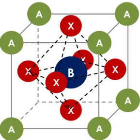
HOIPs are one of the most promising photovoltaic materials of today, showing high efficiencies while using relatively simple fabrication processes, low cost and potential roll-to-roll applica-tions[22], [23]. The basic HOIP, ABX3, crystalline structure is displayed in Figure 1.1.
2D Optimization of Thin Perovskite/Silicon Four-Terminal Tandem Solar Cells
3 The Achilles heel of these novel absorbers is the medium- and long-term stability – having the famous long life of c-Si to compete with – as they are heavily affected by moisture. Moreover, the most common architectures rely on a light-degradation inducing material (TiO2) as elec-tron-transport layer (ETL) and an organic Li-doped material (Spiro) as hole-transport layer (HTL)[6], [7], [24], [33], [35]–[37]. The large area mechanical strength of mainstream architec-tures is also very low, although the use of inter-nal hexagointer-nal scaffolds shows great prom-ise[38].
Despite their drawbacks, interest in HOIPs
soared rapidly and if their stability issues are successfully tackled, can become one of the most prevalent semiconductors of today.
1.3
Tandem solar cell architectures
Tandem devices have traditionally been restricted to niche applications, due to them being heavily based on III-V semiconductors. These are undesirable in terms of cost for most commercial ap-plications[39], being mostly employed in niche scenarios, e.g. space applications[40].
With a bandgap of 1.1 eV, c-Si cells are nearly ideal for the role of low bandgap bottom absorbers[41], requiring as a top absorber partner for a two-junction cell semiconductors with a high bandgap in the 1.7 to 1.8 eV range[9]. High bandgap semiconductors are difficult to come by, with the most prominent candidates being III-V materials which, as mentioned, are notori-ously costlier than silicon and thus are not quite economically viable[4]. It is in this niche that the recent interest in low-cost perovskite absorbers for this role rises, as a straightforward stoichiom-etry of 2:1 bromine to iodine in the standard CH3NH3Pb(I1-xBrx) gives a near ideal bandgap of 1.76 eV[29], [42]. Extensive studies have been performed on the marriage of these materials, and experimental results are promising, having H. Snaith’s company Oxford PV recently reported a 27.3% efficiency, certified by ISE[43]–[48].
Tandem cells can be architected in several configurations, and each has its pros and cons. Those that are considered most important are described here and their benefits compared.
X
X
X
A
A
A
A
A
A
B
X
X
X
A
4
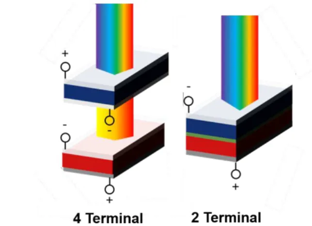
The architecture where upon this work is built is the four-terminal tandem (4T), where two cells are separately fabricated and afterwards mechanically stacked. A schematic of this kind of device is shown in Figure 1.2. From a fabrication point of view, this is the simplest way of achiev-ing a heterojunction. Each sub-cell is separately manufactured, thus allowachiev-ing for the optimal fab-rication conditions for each cell. This is otherwise not possible for architectures where the cells are built on top of each other, as the more direct alternative, the monolithic two-terminal tan-dem[4], [5], [9], [10], [20], [49]–[52]. The 4T structure requires four electrodes, three of which require high transparency and can be sources of parasitic absorption in these devices, a major drawback pointed at this design. From another standpoint, however, the electrical independence of the two sub-cells allows the operation of these at their maximum power points (MPP), making the device less sensitive to variations of the incident radiation [4], [5], [10], [49], [52]
In the two-terminal tandem (2T) architecture (Figure 1.2), only two electrical contacts are considered, as the sub-cells are monolithically integrated and connected in series, with a separat-ing tunnel junction in between. This architecture uses less material than the latter, as only 2 con-tacts are required. A mere transparent contact is required and as such the device is less prone to parasitic absorptions. Kirchoff’s law determines that the device will have a voltage equal to the sum of the sub-cell voltages – which in turn reduces the resistive losses of the system[41]. The series connection limits the current in the system, where the maximum current is determined by the sub-cell with the lowest current. The device must be designed in order to minimize the current mismatch. For optimal performance the device would require specific design specifications for where it would be placed, geographically, which is not feasible from a manufacturing and com-mercial standpoint. Comparing with the 4T model, the processing is also more complicated, as the manufacturing steps of the top cell need to be compatible with the bottom cell layers, as to not affect performance. The bottom cell must also act as a suitable substrate for the top cell to minimize interfacial defects[4], [5], [10], [20], [49]–[51].
2D Optimization of Thin Perovskite/Silicon Four-Terminal Tandem Solar Cells
5
1.4
Material Modelling
The computational modelling of materials dates back its roots from World War II when Jon Von Neumann and Stan Ulam started using simulation methods to determine the behavior of neutrons in alternative to traditional trial-and-error methods, that were deemed too costly, giving birth to the popular Monte Carlo method [53]. Since the 1940’s, computational power has exponentially grown, and more complex simulation of materials and its behaviors are now possible.
Today, material modelling tools are necessary in science and engineering projects to elim-inate trial-and-error loops when developing new materials, device architectures, manufacturing processes or components. The physical behavior of multiple cases can be predicted through sim-ulation of atomic to macroscopic problem, reducing the number of complicated and expensive experiments that would otherwise be necessary.
Here, finite elements (FEM) and finite-differences time-domain (FDTD) methods are em-ployed to model rather complex photovoltaic devices, through commercial software distributed by Lumerical Solutions Inc. – namely Lumerical FDTD and Lumerical DEVICE.
The common characteristic of these numerical formalisms is that both methods require a volume discretization. However, while FDTD uses a structured mesh, FEM relies on an unstruc-tured one, which allows it to solve fine and complex geometric details. In FEM, the system is divided in several units (finite elements) or nodes that are all linked together. The possibility of local mesh refinement allows FEM to tackle more complicated geometries[54].
2D Optimization of Thin Perovskite/Silicon Four-Terminal Tandem Solar Cells
7
Chapter 2:
Simulation methodology
2.1
Finite-differences time-domain method
The study started with an optical simulation setup, provided by Lumerical Solutions Inc. FDTD-formalism based software, commonly used in photonics[55]. The FDTD method was proposed for the first time by Yee[56]. It can be a computationally demanding method, while simultane-ously relies on a comprehensive working principle that makes it a popular tool for solving several electromagnetism problems[54].
From Maxwell’s theory of electromagnetism, the Ampere’s and Faraday’s laws are ex-pressed as following:
∇ × 𝑬 = −𝜇𝑚𝜕𝑯𝜕𝑡 (1)
∇ × 𝑯 = 𝜖𝜕𝑬
𝜕𝑡 + 𝑱 (2)
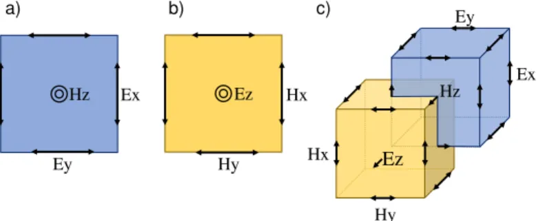
where E is the electric field, H magnetic field, µm the permeability, t time, ε the permittivity and J the current density. The curl operators describe a spatial variation of the fields and, from the above equations, are also coupled to a time variation, resulting in a time-varying magnetic field (H-field) that leads to a rotational electric field (E-field). This results in the basic FDTD time-stepping relations, where the E-field at an initial time permits the calculation of the H-field at this given time[54]. A schematic of the cartesian Yee cell used in FDTD is presented in Figure 2.1.
Figure 2.1: Illustration of the discretization performed in the FDTD method. a) 2-D, H-field along the axis; b) analog case, E-field along the axis.; c) 3-D Yee grid.
Hz Ex
Ey
Ez Hx
Hy
Hy Ez Hx
Hz Ex
Ey
8
This scheme proposed by Yee is still used at the core of most FDTD software and is named the Yee lattice. The vector components of each field are spatially staggered on unit cells of rec-tangular nature, in a way that each E-field vector component is midway placed between a pair of H-field vector components[54].
2.2
Finite elements method for charge transport
Lumerical DEVICE employs a numerical discretization method to solve the constitutive equations of device physics over a finite-element mesh that represents a semiconductor device. The mesh stores the values of all physical quantities throughout the device, including impurity concentrations (ND, NA), carrier concentrations (n,p), and electrostatic potential (φ); and also specifies which boundaries of the device are electrodes. Upon calculating the state of the mesh that satisfies the device-physics equations, DEVICE Charge solver records the current and voltage of each electrode. By repeating this procedure over aa a sweep over a certain range of electrode biases, the I–V behavior of the device can be simulated. Given that 4-Terminal solar cells are being simulated, this process was individually performed for the top and bottom cells. The gen-eration rate is imported from the optical solver, Lumerical FDTD.
As these simulations sought steady-state solutions under drift-diffusion carrier transport, for which the constitutive equations of device physics are the drift-diffusion, Poisson and continuity equations:
𝑱𝑛,𝑝 = 𝑞 𝜇𝑛,𝑝𝑬𝑛/𝑝 ± 𝑞𝐷𝑛,𝑝∇𝑛/𝑝 (3)
−∇ ∙ (ϵ∇𝐕) = qρ (4)
𝜕𝑛/𝑝
𝜕𝑡 = ±
1
𝑞∇ ∙ 𝑱𝑛,𝑝− 𝑅𝑛,𝑝 (5)
here R is the net recombination rate (n and p subscripts indicate electron or hole, respectively), q the electron charge, n/p the electron/hole carrier density, ρ the charge density, µ mobility, D dif-fusivity, V the electrostatic potential and finally C, the ionized impurity density. R=Rn=Rp since the considered processes associated with the material are assumed as equivalent when applied to both holes and electrons.
2D Optimization of Thin Perovskite/Silicon Four-Terminal Tandem Solar Cells
9
Chapter 3:
Results and discussion
When considering 4T tandem architectures where each sub-cell is electrically independent or de-coupled, the constituent cells require a physical separation layer that is both non-conductive and an optical coupler. The former guarantees that the sub-cells are insulated from one another, and the latter that the transmission from the top cell’s unabsorbed light is maximized.
To explore how the interlayer plays a role in the device, an ideal, non-absorbing, material was considered. The refractive index and thickness of this abstract material were varied to maximize the photocurrent on the thin c-Si bottom layer. This is measured by the equivalent Jsc in the target layer. This approach should establish some design rules for the choice of interlayer materials to be employed in tandem architectures.
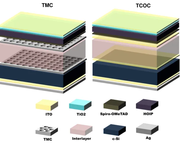
The interlayer is optimized for two device architectures: a standard one with all-TCO con-tact layers – namely indium tin oxide (ITO) – and the alternative one, where the interlayer’s sur-rounding ITO contacts are replaced with idealized metallic contacts, previously introduced. These will be referred throughout this work as transparent conductive contacts (TCOC) and transparent metal contacts (TMC). Both TCOC and TMC architectures are shown in the schematic present in Figure 3.1. The metal-based contacts are assumed to exhibit total transparency and permit direct contact between the interlayer and surrounding materials. Here, a possible replacement of TCO contacts is evaluated, giving preference to various types of metallic nano- and micro-structured contacts exhibiting high transmittance in the desired 700-1100 nm range[5], [11]–[17], [57], [58]. A full replacement of the TCO in lieu of the metallic contacts is not considered in this study, as the perovskite solar cell benefits from an anti-reflection effect introduced by the top ITO contact, which counterbalances the parasitic absorption, as previously concluded by Topic et al[57]. With the removal of the top ITO contact, another anti-reflection coating (ARC) should be implemented. In that case, fluoride glasses should be considered, as the popular MgF2 for this purpose, which have medium refractive indexes (~1.5) and are transparent [59].
10
A standard PSC is considered for the top absorber where perovskite presents a 1.75 eV bandgap, optimal for silicon tandems[4], [9]. A thin silicon cell is considered as the bottom cell. This choice of bottom cell derives from recently shown devices built on ultra-thin mono-crystal-line silicon wafers[61], [62]. These c-Si wafers are considered prime candidates for high effi-ciency thin cells through LT implementations, given that their thickness should enable high ab-sorption enhancements, as predicted by analytical methods with geometric optics in mind, ana-lyzed in Section 3.3, where the Lambertian light scattering limit is calculated for the bottom cell.
Figure 3.1: Schematic representative of the two architectures considered. The con-tacts that border the interlayer are different for each case: at the left, transparent metal contacts (TMC) are employed and at the right, standard TCOC design.
The optical constants were taken or adapted from the literature, as seen in Table 3.1. The HOIP’s refractive index was adapted by blue-shifting the optical constants 0.18 eV. This is in accordance with recent experimental findings on higher band-gap perovskites that agree with a complete blue-shift of the absorption coefficient as utilized here and previously by Saliba et al.[5], [63]. The thicknesses of the involved layers are also discriminated in Table 3.1. The experimental
ITO TiO2 Spiro-OMeTAD HOIP
TMC Interlayer c-Si Ag
2D Optimization of Thin Perovskite/Silicon Four-Terminal Tandem Solar Cells
11
optical data of each material are further presented in Annex I, together with the shifted HOIP refractive index.
Table 3.1 Source of optical material data used in the simulation and respective layer thicknesses.
Material Thickness (nm) Refractive index
In2O3-SnO2 80 (top) 100 (else) Extracted[64]
TiO2 10 Extracted[65]
CH3NH3PbBrxI1-x 500 Adapted[66] Spiro-OMeTAD 100 Extracted[43]
Si 1500 Extracted[67]
Au 200 Extracted[67]
Interlayer 0 to 2500 1.2 to 3.2
3.1
Validation of the simulation setup
Before considering any results from simulations, validation of the model is required. Here, a pre-liminary study on the influence of the wavelength discretization is made, using the popular ana-lytical transfer-matrix formalism, comparing the calculations done by this method with those re-sulting from the numerical simulations.
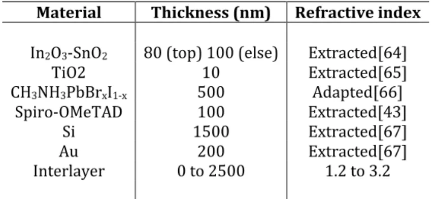
In Lumerical Inc’s FDTD solver, the wavelength discretization of the used light-source is defined by the number of frequency points (nf) used. Given that the points used directly affects simulation time as well as accuracy, a conciliation should be done between these aspects. Simu-lation accuracy becomes of greater importance when interference patterns are expected to be pre-sent, result of nano- and micrometric structures. Simultaneously, data resolution is significant when looking into periodic behaviours, as the period of these can be misinterpreted due to insuf-ficient sampling rate, something well known and pointed at by Shannon and Nyquist sampling theorem[68]. This problematic can be perceived in Figure 3.2a), where the power absorbed on a 500 nm perovskite / 15 µm c-Si tandem is shown for different frequency point values, and differ-ent patterns materialize. The effect is more pronounced at wavelengths that interact with the sili-con layer, which is notorious for its Fabry-Pierot interference patterns[69] .
The equivalent short-circuit current (Jsc) of both cells was chosen as a figure of merit due to its direct relation with the absorbance, as described by the following equation:
12
where λ is the wavelength, h the Planck constant, c the speed of light, A is absorption, and IAM1.5(λ) the irradiance given by the AM 1.5G spectra. Hence, a sweep evaluating the Jsc as a function of points used was fashioned, as shown in Figure 3.2b).
Figure 3.2 : a) Absorption in the tandem structure for different values of frequency points. b) Short-circuit current density as a function of the number of used frequency points (represented by nf); at the bottom a 15 µm thick silicon bottom cell case; at the top a 1.5 µm thick silicon bottom cell case.
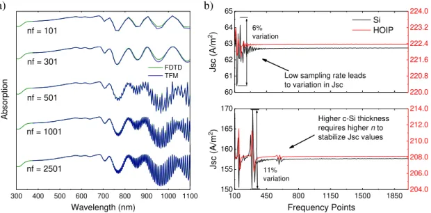
A maximum variation of 11% is seen for the 15 µm Si layer, followed by 6% in the thinner 1.5 µm variant. The perovskite cell does not exhibit much of absolute variation in the Jsc, mainly due to its strong linear absorbing properties. The Jsc value stabilizes at around 500 points for the thinner device, and 700 for the thicker one. Taking these findings into account, a fixed 1001 frequency points was set for every simulation performed henceforth and again the TM-resulting profiles were compared with the numerical results, shown in Figure 3.3.
These show FDTD calculated absorption spectra to accurately match those calculated ana-lytically by the TM method. Therefore, one can consider that the simulations performed here are in accordance from a computational point of view.
300 400 500 600 700 800 900 1000 1100
nf = 101
FDTD TFM
nf = 301
nf = 2501 nf = 1001 nf = 501
Absorpt ion Wavelength (nm) 60 61 62 63 64 65 Jsc (A/m 2)
Low sampling rate leads to variation in Jsc
220.0 220.8 221.6 222.4 223.2 224.0
100 450 800 1150 1500 1850
150 155 160 165 170 6% variation Si HOIP Frequency Points Jsc (A/m 2)
Higher c-Si thickness
requires higher n to
stabilize Jsc values
11% variation 204.0 206.0 208.0 210.0 212.0 214.0
2D Optimization of Thin Perovskite/Silicon Four-Terminal Tandem Solar Cells
13
Figure 3.3: Absorption spectra for the planar devices, resulting from FDTD simula-tion and transfer-matrix method. a) TMC variant; b) TCOC case.
3.2
Planar device: optical simulations for interlayer
optimiza-tion
As previously mentioned, one of the purposes of this study is to optimize the thickness and re-fractive index of the interlayer. This is a critical component of multi-terminal heterojunction solar cell, ultimately defining the transmittance efficiency and electrical insulation between sub-cells[4], [9], [52]. A non-absorbing polymeric material would be ideal here, and to emulate this the extinction coefficient, k, was set to 0. The index was set, as referred in Table 3.1, from 1.2 to 3.2 and the thickness was varied from 0 (no interlayer) to 2 µm.
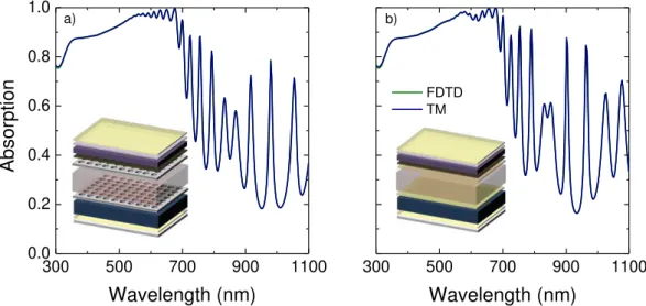
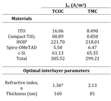
The optimal interlayer is pursued for both the TCOC and TMC designs, and the corre-sponding sweeps are represented in Figure 3.4. The optimal parameters and equivalent Jsc for each layer are shown in Table 3.2. The optimization leads refractive indexes of 2.13 and 1.36 for the TMC and TCOC, respectively. A sharper maximum bottom-cell Jsc of 65.40 A/m2 is noted for TMC design, compared to the 61.20 A/m2 of the TCOC - a relative 6.42% increase. Simultane-ously, the total parasitic absorption observed is 30% lower in the TMC device. The drop in para-sitic absorption is linked to the outright removal of two ITO layers and the consequential elimi-nation of their contribution to this metric. The reflection profiles for each scheme are also pre-sented in Figure 3.5, providing further insight on the device’s behavior, and are analyzed ahead.
Returning to the optimized refractive index values, it is observed that for the TCOC design, values lower than ITO’s index are preferable in lieu of those that would optically match the
sub-300 500 700 900 1100 0.0
0.2 0.4 0.6 0.8 1.0
300 500 700 900 1100
Wavelength (nm)
a)
Absorpti
on
Wavelength (nm)
14
cells (Figure 3.4). This is a curious observation and can be explained by two factors: the first being that ITO itself is not a remarkable optical matcher between spiro-OMeTAD (n~1.6) and c-Si (n~3.6) in the 700-1100 nm range, followed in second by the low absorptivity of silicon in the NIR[10], [67]. These two factors explain why it is advantageous to introduce a low index material between the two ITO contacts – increasing the absorption in the c-Si by at the cost of less trans-mitted radiation from the top cell, by virtue of internal reflections in the considered interfaces. This situation leads to better performance than a simple optical matching, else the optimal inter-layer thickness would converge to 0. The TMC variant is less complex and the interinter-layer simply converges to an index matching value between the c-Si and spiro-OMeTAD. In Figure 3.6 a sim-plified schematic of the light’s path in each structure is presented to better illustrate why each optimal index converged to such different values.
Figure 3.4: Contour plots of the bottom layer’s Jsxin function of the interlayer’s re-fractive index and thickness. At the top, the TCOC case and at the bottom the TMC case.
0 250 500 750 1000 1250 1500 1750 2000 Thickness (nm)
2D Optimization of Thin Perovskite/Silicon Four-Terminal Tandem Solar Cells
15
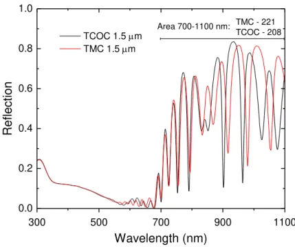
The bottom c-Si absorber - a material with a low absorption coefficient in the NIR re-gion[67] – is not seen as an excellent performer (Table 3.2). This observation is further exacer-bated when comparing c-Si with the remaining layers –where it’s absorption accounts for merely 20.01% of the light absorbed in the TCOC device and 21.84% in the TMC. This leads to an overall anemic efficiency of the bottom cell, <1.6% for either case. In fact, when examining the reflection figures (in both TCOC and TMC), shown in Figure 3.5, a large portion of NIR radiation is re-flected, i.e. not absorbed.
Integrating the reflection in the 700-1100 nm range, it is seen that more light is reflected in the TMC case than for the TCOC design (TMC’s 221 vs TCOC’s 208). This not unexpected, given that while it was seen that the c-Si cell has a higher photocurrent figure than the TCOC, there was a steep decrease in the parasitic absorption (see Table 3.2) and that multiple passes are occurring in the bottom TCOC cell (see Figure 3.6) that, while providing some heightened c-Si absorption, can also lead to higher parasitic absorption by the ITO contacts. This suggests that the higher bottom cell absorption (in the TMC case) is mostly due to the index matching scenario provided by the interlayer’s refractive index of 2.13, and that the parasitic absorption is not the major hinder of the silicon’s performance in this ultra-thin bottom cell scenario. Even when ig-noring the parasitic absorption, the optical performance of the TCOC design is hindered by the application of ITO as middle contacts by poor optical matching in the considered 700-1100 nm range.
Figure 3.5: Reflection profile for the TCOC (black) and TMC (red) cases, considering the optimized interlayer values.
300 500 700 900 1100
0.0 0.2 0.4 0.6 0.8 1.0
TCOC 1.5 m TMC 1.5 m
Wavelength (nm)
Reflection
16
Figure 3.6: Simplified scheme of the optical path in each design. a) TCOC case, the complexity of the ITO/Interlayer/ITO interfaces give rise to internal reflections, benefited by the low interlayer index, aiding the silicon’s absorption. b) TMC, simpler case of index matching where an intermediate value is found as optimal, optically matching the top and bottom cells.
Nonetheless, the future belongs to those who prepare it today, and thus it should be noted that lowering the parasitic absorption gives more room for bottom cell absorption in future itera-tions of the architecture, when light management techniques are considered and employed. This will be further verified in a future section.
Table 3.2: Summary of equivalent absorptions and optimal interlayer parameters for both the TCOC and TMC cases.
Jsc (A/m2)
TCOC TMC
Materials
ITO 16.06 8.490
Compact TiO2 00.89 0.850
HOIP 221.70 218.01
Spiro-OMeTAD 5.58 6.47
c-Si 61.13 65.35
Total 305.52 299.21
Optimal interlayer parameters
Refractive index,
n 1.36* 2.13
Thickness (nm) 160 81
Spiro-OMeTAD Interlayer Silicon ITO ITO Silver n ~1.8
n = 1.36 n ~1.6
n ~3.6 n ~1.8
Interlayer
Silver
n = 2.13
TCOC
TMC
Silicon n ~3.6
Spiro-OMeTAD n ~1.6
a)
b)
2D Optimization of Thin Perovskite/Silicon Four-Terminal Tandem Solar Cells
17
To assess if the previous interlayer optimization was, in fact, accurate for a higher c-Si optical path length (OPL), an arbitrary interlayer thickness was considered (500 nm) and upon that the interlayer’s refractive index was varied from 1 to 3. The resulting sweep is shown here in Figure 3.7 and go in accordance with the previous analysis. In the TCOC case, a low interlayer index remains preferred, whereas the TMC interlayer converged to a higher – index matching – value.
Figure 3.7: Equivalent 15 µm bottom cell Jscin function of the interlayer’s refractive index. The interlayer thickness is set to 500 nm. Similar or equal values to the previous optimization are found as best for each design.
3.2.1
Absorption profiles
Most state-of-the-art perovskite/silicon tandem devices, especially those with record efficiencies involve novel silicon heterojunction (SHJ) solar cells as the complementary absorber to the per-ovskite[4], [5], [10], [49], [52]. These designs, however, are in the range of hundreds of microns in total thickness making the thought of flexibility impossible, absorbing the majority of the NIR radiation in the silicon bulk thickness[57]. This thought is what lead to the consideration of such thin silicon thicknesses in the bottom cell that, as commented before, perform poorly by them-selves. However, the analysis of the absorption profiles of these should be analyzed to establish further optimization guidelines.
18
thermalization losses of high energy photons and maximize the possible device’s efficiency, which ultimately is the main objective of any tandem configuration.
Figure 3.8: Absorption of both designs (TMC and TCOC), with optimized interlayer.
Still considering the HOIP absorber, higher NIR absorptions are seen in the TCOC device. This is thought as a result of the internal scattering behavior that occurs in the interlayer (see Figure 3.6), possibly leading to higher dwell times of NIR photons in the top cell when compared to the TMC design, hence a higher absorption figure.
It is seen that the absorption in the 900-1100 nm range is higher for the TMC’s bottom cell, which coincides with the wavelengths where the material’s absorption coefficient and refractive index are lower. In this region, the optical matching of the TMC case serves the bottom cell best, reflecting on the higher performance. It is also in this region that a sharp reduction in parasitic absorption is seen. In the TCOC design, light is reflected multiple times in the ITO/Interlayer/ITO interfaces and, while it appears to bring a positive effect for the silicon’s absorption, it also leads to higher parasitic absorption by the ITO contacts. The removal of ITO leads to a slightly higher spiro-OMeTAD absorption – justified by the simple higher availability of absorbable radiation.
0.0 0.2 0.4 0.6 0.8 1.0
300 500 700 900 1100
0.0 0.2 0.4 0.6 0.8 1.0
Abs
orption
TMC
Abs
orption
Wavelength (nm)
Total Si Perovskite Parasitic
2D Optimization of Thin Perovskite/Silicon Four-Terminal Tandem Solar Cells
19
These interlayer optimizations allow the narrowing of the parameters for future integration with light trapping (LT) structures. A widely studied field, LT implementations strive to increase the optical path length in solar cells by significant values and increasing the absorption of the semiconductor. thus, employing novel light trapping structures in the fashion of plasmonic nano-particles, Mie-scattering spheroids or even simple pyramidal texturization, would enhance the NIR response of the device and consequently increase its efficiency even in this thin architecture scenario[18], [55], [77], [78], [60], [69], [71]–[76].
In the following section, the performance of a bottom cell with integrated LT is predicted through analytical and numerical methods. First the Lambertian LT limit is analytically calculated for a range of crystalline silicon cell thickness, in the 700-1100 nm wavelengths to examine the potential of the bottom cell. Subsequently, a lower limit of the previous analysis is chosen as the maximum optical path length gain for this study’s cell of 1.5 µm thick, and the optoelectronic performance of the sub cell is evaluated for the OPLs leading to the maximum chosen (15 µm).
3.3
Ray optics path length limits in bottom c-Si cell
It was verified that in a planar device, as predicted, the bottom 1.5 µm cell shows weak absorbance in the NIR region. This shortcoming can be tackled through advanced light management tech-niques, or through outright increasing the silicon’s thickness. In this section, the possible gains of the implementation of LT mechanisms are explored. Light trapping methodologies allow higher absorption figures in the semiconductor in question, by means of OPL increase or through the creation of high E-field intensity regions or localized modes.
The optimized parameters that were found and discussed in the previous section, shown on Table 3.2, were used for the remainder of the simulations performed in this work. Thus, the TCOC cell, a refractive index (n) of 1.36 together with 160 nm of thickness was considered for the in-terlayer, and in the TMC variant, n was set to 2.13 and the thickness to 81 nm.
20
In indirect bandgap semiconductors, due to the need of emission of a phonon during the absorption of near-bandgap photons, the probability of absorption of these is severely reduced, increasing their penetration depth [79], [80]. This reflects on the observed absorption figures of direct and indirect semiconductor – the former need reduced thicknesses to absorb a great part of the sunlight, while the latter need higher thicknesses. This is no different for c-Si, and thus for thin absorber thicknesses like those studied here, LT is of paramount importance to ensure the viability of the device. It is of even more importance when we consider that c-Si is here considered as a bottom cell, and the wavelengths that are meant for absorption are those which need higher dwell time in the material. While these statements may paint a grim picture for the application of thin c-Si wafers, it should be noted that these allow for flexible devices, are lighter than standard SHJ cells , can be cheaper and show enhanced electrical properties – as lower bulk recombination – and even reduced light induced Staebler Wronski degradation [81], [82].
2D Optimization of Thin Perovskite/Silicon Four-Terminal Tandem Solar Cells
21
Figure 3.9: LT scheme with a Lambertian back reflector.
Integrating the solar spectrum in the 700-1100 nm range, the maximum photogeneration is found to be 233.3 A/m2. The analytical data presented in Figure 3.10 show that a 30 µm cell with ideal Lambertian LT presents a Jph of 228.9 A/m2. It is therefore logical, that for thicknesses > 30 µm, the observed theoretical photocurrent gains are minimal. This observation goes very much in accordance with those made by Shockley, where he stated a 30 µm c-Si wafer is sufficient for high-efficiency single-junction solar cell. These observations indicate that ultra-thin c-Si cells may be in fact ideal for the bottom absorber role, as the reduced thicknesses mean higher carrier collection efficiency as the carrier diffusion length required for collection is, consequently, lower.
Figure 3.10: Bottom cell analytically determined photocurrent. The comparison for a no-LT case and the Lambertian limit is shown, and the possible gains on a 1.5 µm c-Si slab. The case for 30 µm c-Si cells is also pointed out. The Lambertian LT absorption of the 1.5
µm cell is equivalent to a non-LT cell with 17 µm thickness (pointed out by the dashed line).
θ
Loss cone
Internal
reflection
Texturized back reflector
22
3.4
Complete optical and electrical solar cell simulations
In this section, the results of electrical simulations are used to evaluate the theoretical electrical performance of the device. These simulations are an important part of the established optoelec-tronic model and present great potential in the optimization of photovoltaic designs. To demon-strate the capabilities of the model, here they were also employed to assess the best doping orien-tation of the silicon bottom cell, n+– p - p+ or p+- p – n+. The scope of this portion of the model is not as extensive as the optical part, but nonetheless demonstrate its usefulness.
The physical quantities that best evaluate the performance of a solar cell are mainly the efficiency and fill-factor (FF) which are calculated using the following equations:
𝐹𝐹 =𝐽𝑀𝑃𝐽 × 𝑉𝑀𝑃
𝑠𝑐× 𝑉𝑜𝑐 (2)
𝜂 =𝐹𝐹 × 𝑃𝑃 𝑚𝑎𝑥
𝑠𝑜𝑙𝑎𝑟 (3)
where, V the voltage, P is the power in W/m2. The “MP” subscript indicates the maximum power point. The “solar” subscript the irradiance that is commonly approximated to 1000 W/m2.
An optical thickness of 15 µm was taken in consideration for the absorption spectra further analyzed and shown in Figure 3.12, as it is within the previously calculated Lambertian limit (LT 1.5 µm = no-LT 17 µm), and constitutes a feasible OPL increase when taking into account modern LT approaches[60], [74]–[76]. It should be noted that the presented absorption profiles are not of a true light trapping scenario, but of a thicker silicon cell. This was the chosen approach to emulate the increase in OPL. Nonetheless, one can find value and make projections of the device’s re-sponse when looking into the absorption profiles and the behavior of the layers involved anyway.
2D Optimization of Thin Perovskite/Silicon Four-Terminal Tandem Solar Cells
23
were sourced from the literature in similar fashion[91] and the parameters for c-Si were directly used from the software’s database.
Table 3.3: Physical parameters considered in the electrical simulations. + Spiro-OMeTAD. XShockley-Read-Hall recombination. oCarrier mobility. #effective mass. Φ is the work function.
In Table 3.4 the absorption of each layer, for the 15 µm Si bottom cell, is shown through equivalent short-circuit current density values. The total perovskite absorption drops, compared to previously obtained values, seen in Figure 3.8 and Table 3.2. This is likewise observable in the absorption and reflection profiles (Figure 3.11 and Figure 3.12). Due to less back-reflected radi-ation travelling from the bottom cell to the top of the device (versus the no-LT scenario), the perovskite layer loses most of the ˃700 nm absorption. This reinforces what was discussed in Planar device: optical simulations for interlayer optimization, that the perovskite’s high Jsc figure was inflated due to NIR absorption. This is a consequence of the chosen experimental data (Table 3.1, Figure 4.2). This behavior should not influence the choice of the best design here, as the absorption properties of perovskites post bandgap may vary with many factors.
Therefore, to eliminate this variation from the choice of which is the best design, the least NIR absorbing perovskite was considered when calculating the combined efficiency of the device.
HOIP TiO2 Spiro+ ITO c-Si
Fundamental Prop.
dc permittivity 6.5 9.0 3.0 - 11.7
Φ (eV) 3.93 4.50 3.80 4.50 4.59
Eg (eV) 1.75 3.20 2.30 - 1.11
#m*
e 0.10 1.18 0.05 - 1.18
#m*h 1.00 0.81 1.00 - 0.81
oµe (cm2/V s) 10.0 5.0 0.5 - 1471.0 oµ
h (cm2/V s) 10.0 0.2 10.0 - 470.5
XSRHh (s) 10-6 2x10⁻⁸ 2x10⁻⁹ - 4x10⁻⁷ XSRHe (s) 10-8 2x10⁻⁸ 2x10⁻⁸ - 10-6
Doping Properties
Dopant type p n p - n p p
Conc.
(cm-3) 4x10¹⁶ 5x10¹⁷ 1018 -
2x10²⁰ to 1015 2x10¹⁶ 2x10²⁰ to 1010
Profile Const. Const. Const. - erfc Const. erfc
24
This assures that the total device efficiency cannot be linked to the perovskite’s enhanced NIR absorption in detriment of the intended c-Si’s and that only the bottom cell performance influ-ences the result. Thus, the PSC top cell of the 15 µm c-Si TMC device – which is coincidentally, the best performing bottom cell - was chosen. The PSC then presents a 20.49% efficiency figure, which is lower than a state-of-the art 1.57 eV PSC. This is expectable for a higher bandgap cell, which should perform lower than a cell with an ideal bandgap for single-junction applications. Finally, we then see combined device efficiencies up-to 27.08% for the TMC case, and 26.52% for the TCOC, which are both higher than the record Si performance[92].
When a no-LT approach was studied (Planar device: optical simulations for interlayer optimization subsection), both designs performed similarly due to the thin c-Si thickness consid-ered, and the benefits from the index matching interlayer and parasitic absorption elimination were rather insubstantial (see Table 3.2). Only here, by emulating light-trapping techniques, we see the fruits of the labor that was the interlayer optimization and the ITO replacement, observed in the 9% lower reflection and 8% c-Si higher absorption for TMC, when compared to TCOC.
Figure 3.11:Reflection profilesofTMC(red)and TCOC (black) w\10x bottomcell OPL. The 700-1100 nm wavelengths were integrated for comparison purposes.
With the increased performance of the bottom cell, the main contributors for parasitic ab-sorption – ITO and spiro-OMeTAD – absorb less radiation. A difference between the abab-sorptions
300
500
700
900
1100
0.0
0.2
0.4
0.6
0.8
1.0
Reflection
Wavelength (nm)
TCOC 15 mTMC 15 m
2D Optimization of Thin Perovskite/Silicon Four-Terminal Tandem Solar Cells
25
of the ITO and spiro-OMeTAD layers is still noted between the architectures, where the TMC understandably presents less than half the parasitic ITO absorption of the TCOC due to the elim-inated contacts. These layers, particularly the organic spiro-OMeTAD, persist as a substitution priority in perovskite architectures, partly due to the parasitic absorption exhibited by either and the degradation potential presented by the organic layer. Alternatives for hole-transport materials have been searched in the organics and oxides alike – and even the removal of the HTL has been considered -, and further studies should be made in this area[34], [38], [89], [93]–[99]. The de-fining electrical parameters of a solar cell were taken for the various silicon OPLs, results pre-sented in Table 3.5. Further simulations were performed for higher than the Lambertian limit, present in Annex II.
The simulations studying the best doping configuration, n+ p p (referred as nip) vs p p n+ (pin), were ran for the TMC case only since there are no pertinent differences from an electrical performance point of view. The influence of the contacts was not studied here, and ideal contacts were considered for every simulation. In further work, however, the influence of the contact prop-erties should be taken into account. It is found that the optimal configuration is nip, mostly due to the more pronounced absorbance in the back of the cell, as the incident light is mostly
com-posed of wavelengths >700 nm. In that region the absorption coefficient of c-Si is lower and
therefore absorption is done at higher penetration depth. Photogeneration is preferred to occur in the p or intrinsic sections of the material, due to the diffusional nature of the minority carriers (faster diffusing electrons for p, slower holes for n)[80], [100]. For more complex LT implemen-tations these results may be different, and this study serves to remind that different absorption characteristics may benefit from different doping configurations.
Table 3.4: Equivalent short circuit current of the layers of the light-trapping 15 µm c-Si bottom cell design.
Jsc (A/m2)
TCOC TMC Materials
ITO 9.35 4.44 Compact TiO2 0.86 0.85 HOIP 207.85 203.38 Spiro-OMeTAD 3.96 4.59
26
Figure 3.12: Absorption spectra for the equivalent 15 µm sub-cell devices; in the top the TMC case and in the bottom the TCOC.
The simulated PSC open circuit voltage is 1.23 V, which presents interesting possibilities in the overall device configuration. Due to the higher bandgap, this is slightly higher than the already high Voc in standard PSCs, which depend on complex defect physics[90]. This value is roughly double that of silicon cells – as reinforced by the simulation results in Table 3.5 – allow-ing for a two bottom cells in series, parallel with one top type of configuration. This is illustrated in Figure 3.13 a) and b) and represents a voltage matching internal circuit, where the bottom cell is split in two separate cells, united in series to sum their voltages, which in turn are parallel with the top. Considering negligible resistive losses, operation at maximum power point (MPP) and perfect voltage matching, the performance of the tandem module can be estimated by a rather simple current sum case, accounting for the voltage-matching configuration previously men-tioned. For a 1 cm2 cell, the output IV curve of the idealized device is shown in Figure 3.13 c).
0.0 0.2 0.4 0.6 0.8 1.0
300 500 700 900 1100
0.0 0.2 0.4 0.6 0.8 1.0
Abs
orption
Total Si
Perovskite Parasitic
Abs
orption
Wavelength (nm)
TMC
2D Optimization of Thin Perovskite/Silicon Four-Terminal Tandem Solar Cells
27
Table 3.5 : Solar I-V curve characteristic of various optical path lengths of the silicon bottom cell, for both the micro-mesh and TCO case, together with the less absorbing PSC.
O.P.L (µm) VOC (V) Jsc (A/m2) Pmax (W/m2) FF (%) Eff. (%)
TMC (nip)
1.5 0.57 33.6 15.7 82.00 1.57
3.0 0.58 57.8 27.7 82.15 2.77
5.0 0.59 101.5 50.1 82.92 5.01
15.0 0.60 132.3 65.9 82.49 6.59
TMC (pin)
1.5 0.56 33.4 15.6 82.38 1.56
3.0 0.58 57.3 27.4 82.10 2.75
5.0 0.59 99.8 49.2 82.93 4.92
15.0 0.60 128.5 63.9 82.57 6.39
1.5 0.56 30.5 14.1 82.00 1.42
3.0 0.58 52.6 25.0 82.00 2.50
TCOC 5.0 0.59 92.6 42.6 82.95 4.56
15.0 0.6 121.4 60.3 82.68 6.03
PSC
(TMC, 15 µm)
0.5 1.23 197.5 204.8 84.33 20.49
Figure 3.13: a) Equivalent electric circuit of the module b) Schematic of the 1 cm2 tandem unit cell and c) output IV curve of the device and the sub-cells (15 µm TMC case). The tandem (blue) is displayed, and results from the sum of the 0.5 cm2 Si cells in series (full red) with the PSC (green). As a comparison, a 1 cm2 c-Si cell IV curve is shown (dash red). The tandem IV is calculated considering ideal series/parallel resistances between cells.
Jph
Jph Jph
Top-Cell
Bot-Cell Bot-Cell
a)
b)
Tandem
FF (%) 81.89
η (%) 27.02
Isc (mA) 26.01 VOC (V) 1.23
Perovskite topcell Si bottom cell Si bottom cell
+
-1 cm2
0.5 cm2 0.5 cm2
28
3.5
Results summary and analysis
Until now, the most remarkable perovskite/silicon tandem configurations that have been designed were done so bearing in mind pre-existing commercial SHJ silicon modules, where the perovskite top cell would be placed on top. While this is probably the most likely format which PSCs will introduce themselves on the PV market, the happy marriage of these materials should not end here. Together, significantly thin solar cells capable of joining high efficiency and flexibility are achievable, after some of the presented obstacles to the architecture are surpassed.
One of the pointed problematics in 4T architectures is on the parasitic ab-sorption that transparent contacts duce. This is tackled here by the intro-duction of the TMC design, which leads to better photocurrent generation in the bottom cell. The chart in Figure 3.14 il-lustrates this, where the differences be-tween TMC and TCOC are discrimi-nated, for LT and no-LT scenarios. The benefit of the TMC implementation is better seen in the LT cases, where an 8% higher c-Si photocurrent is noted versus the TCOC, together with a 30% lower
parasitic absorption. A lower perovskite absorption is seen in the TMC, indicating less NIR radi-ation being reflected in the bottom layers, indicating that the interlayer design is more effective in this case. With these observations in mind, it can be safely said that the TMC design is better than the traditional TCOC, especially when light-trapping implementation is accounted for.
The LT analysis done in the subsection Ray optics path length limits in bottom c-Si cell suggests that these techniques have the potential of allowing high absorption in a thin silicon slab, complementing perfectly with the ultra-thin film perovskite top cell. Only with LT methodologies are thin and flexible designs legitimized, permitting for bulk-like absorptions in micrometric cells.
These results paint a promising picture for the future of flexible PV and illustrate how the upcoming HOIP materials can revolutionize the energy and mobile electronics market, by bring-ing forth low-cost and thin photovoltaics.
TCOC noLT TMC noLT TCOC LT TMC LT
0 100 200 300 400 Jph ( A /m 2 ) Parasitic Top Bottom 203.38 166.75 153.66 207.85 218.01 65.35 61.13 221.70 8.1% difference 9.87 14,17 15.85 22.69
2D Optimization of Thin Perovskite/Silicon Four-Terminal Tandem Solar Cells
29
Chapter 4:
Conclusion
The strive for low cost, high efficiency photovoltaics whose production can be integrated with existing processes and techniques is one of the most disputed topics in PV research. Additionally, the combination of the previous characteristics with flexible implementations is considered as one of the holy grails of the research community. In this work, the possibility of integrating all these properties is studied, and the findings lead to a promising outlook.
Although depending on further study in light-management techniques for the near-infrared absorption of the silicon bottom cell, the optical path length approximation here used suggests conceivable 27% efficiencies (see Table 3.5). This figure is above that of record monolithic sili-con designs, all in micrometric thicknesses, further demonstrating the elegant blend between per-ovskite and silicon. Furthermore, the performance difference between a standard architecture with contacts comprised of the widely used TCO, indium tin oxide, and idealized metallic contacts (TCOC and TMC) was investigated to further evaluate the performance loss due to parasitic ab-sorption in these common electrical contacts. Comparing these, a 30% drop in parasitic abab-sorption is noted (Table 3.2). When optimizing the interlayer for both designs, it was found that the ideal values of real refractive index or the TCOC and TMC are 1.36 and 2.13, respectively (Figure 3.4 and Table 3.2). It is concluded that the ITO not only is detrimental in terms of unwanted absorp-tion but also hinders the index-matching benefits that the interlayer should bring.
Due to high parasitic absorption figures found in the optical simulations ran in this study, collectively with the degradation properties that influence the perovskite absorber, the organic spiro-OMeTAD material is pointed out as a priority material to be replaced in standard perovskite solar cell architectures, further reinforcing previous conclusions by other authors.
30