Strain behavior of lanthanum modified BiFeO3 thin films prepared via soft
chemical method
A. Z. Simões, E. C. Aguiar, A. H. M. Gonzalez, J. Andrés, E. Longo et al.
Citation: J. Appl. Phys. 104, 104115 (2008); doi: 10.1063/1.3029658
View online: http://dx.doi.org/10.1063/1.3029658
View Table of Contents: http://jap.aip.org/resource/1/JAPIAU/v104/i10
Published by the AIP Publishing LLC.
Additional information on J. Appl. Phys.
Journal Homepage: http://jap.aip.org/
Journal Information: http://jap.aip.org/about/about_the_journal
Top downloads: http://jap.aip.org/features/most_downloaded
Strain behavior of lanthanum modified BiFeO
3thin films prepared via soft
chemical method
A. Z. Simões,1E. C. Aguiar,1,a兲 A. H. M. Gonzalez,1J. Andrés,2E. Longo,1and J. A. Varela1
1
Departamento de Físico-Química, Instituto de Química, Laboratório Interdisciplinar em Cerâmica—LIEC, UNESP, CEP, Araraquara, Säo Paulo 14800-900, Brazil
2
Departamento de Química Física y Analítica, Universitat Jaume I, 12071 Castelló, Spain
共Received 27 June 2008; accepted 9 October 2008; published online 24 November 2008兲
Pure and lanthanum modified BFO 共LaxBi1−xFeO3, x= 0.0, 0.08, 0.15, 0.30兲 thin films were
fabricated on Pt共111兲/Ti/SiO2/Si substrates by the soft chemical method. The effect of La
substitution on the structural and electrical properties was studied. Scanning electron microscopy, x-ray diffraction, and Raman spectroscopy have been employed to characterize the thin films while the piezoelectric measurements were carried out using a setup based on an atomic force microscope. It was found that La-doped BFO thin films exhibited good ferroelectric properties, such as improved leakage current density and retention-free characteristics. The unipolar strain is strongly reduced by the amount of lanthanum added to the system. ©2008 American Institute of Physics.
关DOI:10.1063/1.3029658兴
I. INTRODUCTION
Multiferroic materials have attracted renewed interest in recent years1–5due to both its potential applications for elec-tronic device and its fascinating fundamental physics.6–8 In particular, special attention has been designed for multi-ferroic oxides such as BiFeO3 共BFO兲,
9
BiMnO3, 10
TbMnO3, 11
and TbMn2O5共Ref.12兲due the potential to
pro-vide a wide range of applications, including the emerging field of spintronics,13 data-storage media,14 and multiple-state memories.8These multiferroic materials have simulta-neous ferromagnetic, ferroelectric, and/or ferroelastic ordering.15
The well-known single phase multiferroics are mainly Mn- or Fe-based oxides.16–19Among them, BFO is the only known material that is both ferroelectric共TC⬃1083 K兲and antiferromagnetic共TN⬃625 K兲.
20,21
It has a rhombohedrally distorted ferroelectric perovskite structure共TC= 123 K兲with the space groupR3c.22,23Recent reports of a large spontane-ous polarization 共⬃100 C/cm2兲 in thin films,24 bulk
ceramic,25and single crystals26of BFO have led to an explo-sion of interest in its growth and properties.
The ferroelectric mechanism in BFO is controlled by the stereochemical activity of the Bi3+ 6s2 lone pair, responsible of a charge transfer process from 6s2 to formally empty 6p
orbitals,27,28 while the weak ferromagnetic property can be associated with the residual moment from the canted Fe3+ spin structure.29 The coupling effect between both magnetic and electric behaviors occurs through lattice distortion of BFO共Ref.30兲and Khomskii31has been emphasized the dif-ferent ways to combine magnetism and ferroelectricity in mutiferroics materials.
The structure and properties of thin films are well known to exhibit a number of deviations from those of bulk
ceram-ics and single crystals. The origin of the size-dependent ferroelectric properties remains a challenging problem, and a better understanding as to which extent the bulk physical properties can be used for design of thin-layer devices, is actually required. Retention, which is the time-dependent change in the polarization state of the ferroelectric film, is another factor which limits the life of a ferroelectric memory device. In bismuth-based ferroelectrics, such as Bi4Ti3O12
共Ref. 32兲 and SrBi4Ti4O15, 33
the doping of lanthanum 共La兲 was effective to enhance the insulating and ferroelectric properties because of the reduced oxygen vacancy by the stabilized oxygen octahedron.34 Some studies reported in literature35–37suggest that the inhomogeneous magnetic spin structure can be effectively suppressed by La doping. There-fore, the influence of La doping on polarization switching, ferroelectric reliability, and multiferroic properties of BFO films deserves more attention.38 In this respect, strain engi-neering and functional tuning of thin films are the leading activities for the development of the next generation of elec-tronic devices. Recently, several research groups have sub-stituted Bi by La and Tb in order to study the effect of doping on electric and magnetic behavior of pure BFO and lanthanum doped 共BLFO兲 thin films.39–42 Recently, Zheng
et al.43 presented synthesis and ferroelectric properties of BiFeO3thin films grown by sputtering, while Liet al.
44
em-ployed a cosputtering method to obtain BiFeO3thin films on
Pt/Ti/SiO2/Si substrates.
Our group has expanded significant effort in developing synthetic routes of BiFeO3thin films
45,46
and we have previ-ously reported the preparation of BLFO thin films grown on Pt共111兲/Ti/SiO2/Si substrates with good structural,
micro-structural, and electrical properties by the soft chemical method.9,32,47,48 In the present investigation and as a natural extension of previous work, pure and lanthanum modified Bi1−xLaxFeO3 共x= 0.0, 0.08, 0.15, 0.30兲 thin films were
pre-pared on Pt共111兲/Ti/SiO2/Si substrates by the soft chemical
a兲
Author to whom correspondence should be addressed. Electronic mail: [email protected].
method. Structural and electrical properties of the films, mainly related to strain behavior, were investigated by using various techniques with a view to explore their technological applications.
II. EXPERIMENTAL PROCEDURE
Lanthanum modified bismuth ferrite thin films were pre-pared by the soft chemical method, as described elsewhere.46 The films were spin coated on Pt/Ti/SiO2/Si substrates by a
commercial spinner operating at 5000 rpm for 30 s 共spin coater KW-4B, Chemat Technology兲. An excess of 5 wt%
of Bi was added to the solution aiming to minimize the bis-muth loss during the thermal treatment. The thin films were annealed at 500 ° C for 2 h in the conventional furnace under static air atmosphere. The film thickness was reached by re-peating ten times the spin coating and heating treatment cycles. The thickness of the annealed films was measured using scanning electron microscopy共Topcom SM-300兲at the transversal section. We have obtained films with thickness in the range of 340–360 nm. In this case backscattering elec-trons were used. Phase analysis of the films was performed at room temperature by x-ray diffraction共XRD兲using a Bragg– Brentano diffractometer共Rigaku 2000兲and CuK␣radiation. Raman measurements were performed using an ISA T 64000 triple monochromator. An optical microscope with 80⫻ ob-jective was used to focus the 514.5 nm radiation from a Coherent Innova 99 Ar+ laser on the sample. The same
mi-croscope was used to collect the backscattered radiation. The
FIG. 1.共Color online兲XRD data for BFO films deposited by the polymeric precursor method with different La contents:共a兲x= 0.0,共b兲x= 0.08,共c兲x = 0.15, and共d兲x= 0.30.
FIG. 2. 共Color online兲Micro-Raman spectra for BFO film deposited by the polymeric precursor method and annealed at 500 ° C for 2 h, with different La contents:共a兲x= 0.0,共b兲x= 0.08,共c兲x= 0.15, and共d兲x= 0.30.
scattering light dispersed was detected by a charge-coupled device detection system =0.3 mm. The leakage current-voltage 共I-V兲 characteristic was determined with a voltage source measuring unit共Radiant Technology 6000 A兲. Piezo-electric measurements were carried out using a setup based on an atomic force microscope in a multimode scanning probe microscope with Nanoscope IV controller共Veeco FPP-100兲. In our experiments, piezoresponse images of the films were acquired in ambient air by applying a small ac voltage with an amplitude of 2.5 V共peak to peak兲and a frequency of 10 kHz while scanning the film surface. To apply the external voltage we used a standard gold coated Si3N4cantilever with
a spring constant of 0.09 N/m. The probing tip, with an apex radius of about 20 nm, was in mechanical contact with the uncoated film surface during the measurements. Cantilever vibration was detected using a conventional lock-in tech-nique. Top Au electrodes共0.5 mm diameter兲were prepared for the electrical measurements by evaporation through a shadow mask at room temperature. Retention characteristics of the films were measured by independently observing the time-dependent changes in Pⴱ 共switched polarization兲, and
P∧
共nonswitched polarization兲. For Pⴱ, the capacitor was
switched with a negative write pulse and read by a positive read pulse after retention timet. For P∧
, positive pulses were used for both writing and reading. The pulse width for all triangular pulses was 1.0 ms. The time delay between the right pulse and the first read pulse is referred to as retention time.
III. RESULTS AND DISCUSSION
Figure1 presents the XRD patterns of BFO and BLFO films deposited on platinum coated silicon substrates. The films were well crystallized at a processing temperature of 500 ° C. The BFO film self-organized to produce 共200兲-preferred orientation, while the BLFO film crystallized with random orientation and better crystallinity. With partial sub-stitution of isovalent La ions for A-site bismuth ions, the 共100兲 diffraction peak of the BLFO film shifted toward a higher angle. Increasing lanthanum content leads to an addi-tional peak at 2= 28° that could be assigned to the diffrac-tion peak of Bi2O3, probably formed due to the substitution
of lanthanum by bismuth in the crystal lattice.
An analysis of the evolution of Raman spectra in the lanthanum modified bismuth ferrite shows the order-disorder degree of the atomic structure at short range 共Fig. 2兲. The modes further split into longitudinal and transverse compo-nents due the long electrostatic forces associated with lattice ionicity. Substitution of lanthanum in theA-site of the lattice reduces the distortion of octahedral clusters having little in-fluence in the relative intensity of the bands. The vibrational modes located at 224, 355, 385, 531, and 564 cm−1 result
from the FeO6octahedral共Fe= 5 or Fe= 6兲. The band located
below 200 cm−1 is due to the different sites occupied by
bismuth within the perovskite layer. Raman frequencies are not strongly affected by lanthanum substitution. Slight changes which occur above 200 cm−1 in the BFO can be
associated with structural distortion and reduction in
tions in the FeO5octahedra. Lanthanum atoms substitute
bis-muth within the perovskite structure having marginal influ-ence in the interactions between the 共Bi2O2兲2+ layers and
perovskite.
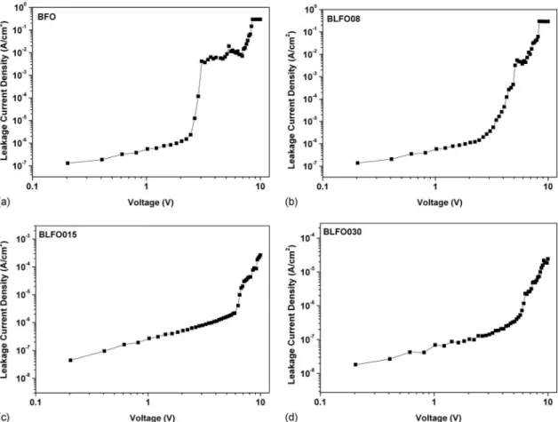
A typical leakage current characteristic for the films is given in Fig.3. The curves were recorded with a voltage step width of 0.1 V and elapsed time of 1.0 s for each voltage, here the measured logorithmic current density共logJ兲versus the logorithmic electric field共E兲is shown. It can be seen that there are two clearly different regions. The current density increases linearly with the external electric field in the region of low electric field strengths, suggesting an Ohmic conduc-tion. At higher field strengths the current density increases exponentially, which implies that at least one part of the conductivity results from Schottky or Poole–Frenkel emis-sion mechanism. The leakage current density at 1.0 V de-creases after substitution for lanthanum. The main reasons for such behavior can be attributed to changes in the surface roughness and reduction in microcracks due the modification in the lattice volume after lanthanum addition. In this way, lanthanum acts reducing the oxygen vacancies and as conse-quence improves the switching process of electrical dipoles. On the other hand, undoped BFO present defects as Bi or Ti vacancies resulting in an increase in conductivity. Therefore, this fact indicates the presence of mobile carriers which are
positively charged and that the possibility of hopping through the Bi ion can be considered. The unipolar strain behavior at room temperature is shown in Fig.4. The unipo-lar strain presents a maximum at 5 kV/cm while the satura-tion regime is reached at 10 kV/cm. Lanthanum decreases the strain behavior, in part, due to domain reorientation. Be-yond that point, it is possible that a modest bias field results in the transition from asymmetric to symmetric phase. This field-induced phase transition may be ascribed to the pinch-ing effect, that is, the consequent decrease in free energy difference among polymorphic phases. A careful inspection of the S−E plots reveals that there are two apparent linear regions at low fields 共E⬍5 kV/cm兲 and high fields 共E
⬎10 kV/cm兲and one transition region, which corresponds to domain reorientation induced by external electric fields. The hysteretic strain could be associated with domain reori-entation. The strain is hysteresis-free at electric fields higher than 5 kV/cm, indicating a stable single domain/poling state induced by the high external electric fields. In addition, from the S versus E profiles, no noticeable induced phase transi-tion is observed at such high electric fields. It is shown that lanthanum reduces the unipolar strain when compared to BFO films, i.e., the strain was共S= 0.16%, 0.12%, and 0.11%兲 and共S= 0.17%兲for lanthanum doped films and BFO, respec-tively. The decreasing of both strain response and strain
en-FIG. 4. Strain response for BFO films deposited by the soft chemical method with different La contents:共a兲x= 0.0,共b兲x= 0.08,共c兲x= 0.15, and共d兲x = 0.30.
ergy after doping process can be associated with the reduced polarizability and the pinning effect. As can be seen, the small strain variations one each curve with electric field can be probably caused by clamping effect due to the stress cre-ated in the film-substrate interface and the existence of an ultrathin air gap between the tip and the sample which might lower the actual voltage drop in the film.
Figures 5共a兲–5共d兲 show the retention characteristics of the films as a function of retention time from 1 to 1 ⫻104 s. The value of initial polarization decayed and
ap-proached a nearly steady-state value after a retention time of 10 s. The small decay of the retained charge in the films is a favorable indication for memory applications. After a reten-tion time of 1⫻104 s, the polarization loss was only about
6% of the value measured at t= 1 s for an applied electric field of 150 kV/cm. Depolarization fields generated by the redistribution of space charge, defects, and dipole charges could be the origin of the polarization decay after writing. For the infant period 共within 10 s兲, depolarization fields could be the main contribution to polarization loss. The de-polarization field increases with increasing the retained po-larization and is time dependent. The long-time retention loss is attributed to the effect of redistribution of defect charges. This effect leads to a small decrease in the polarization by
compensating the polarization charges when the redistribu-tion of defect charges is driven by polarizaredistribu-tion.36The reten-tion failure tests showed that the BLFO films have quite good long-time retention characteristics, retaining 94% of the values measured at t= 1⫻104 s for an applied electric field of 150 kV/cm. Polarization charge compensation by the redistribution of defect charges should be considered to ex-plain this small retention loss in lanthanum doped bismuth ferrite thin films. The results of these studies are very prom-ising and suggest that BLFO thin films are attractive for use as storage element in nonvolatile ferroelectric random access memories.
IV. CONCLUSIONS
Pure and lanthanum doped bismuth titanate thin films were fabricated on Pt substrate using the soft chemical method through annealing at 500 ° C for 2 h. Raman modes are not strongly affected by lanthanum substitution. It was found that lanthanum reduces the strain behavior of BFO films. From leakage current density values we noted that La+3 substitution for Bi+3 is an effective way to reduce
bis-muth vacancies that are accompanied by oxygen vacancies decreasing the film conductivity. The results of these studies
FIG. 5. Retention curve characteristics of BFO film deposited by the soft chemical method with different La contents:共a兲x= 0.0,共b兲x= 0.08,共c兲x= 0.15, and
are very promising and suggest that BLFO thin films can be used as storage element in nonvolatile ferroelectric random access memories.
ACKNOWLEDGMENTS
The authors thank the financial support of the Brazilian research financing institutions: CAPES, FAPESP, and CNPq.
1
N. A. Spaldin and M. Fiebig,Science309, 391共2005兲. 2
W. Eerenstein, N. D. Mathur, and J. F. Scott,Nature共London兲442, 759
共2006兲. 3
S. W. Cheong and N. Mostovoy,Nature Mater.6, 13共2007兲. 4
R. Ramesh and N. A. Spaldin,Nature Mater.6, 21共2007兲. 5
W. Eerenstein, M. Wiora, J. L. Prieto, J. F. Scott, and N. D. Mathur,
Nature Mater.6, 348共2007兲. 6
M. Fiebig,J. Phys. D38, R123共2005兲. 7
G. Catalan,Appl. Phys. Lett.88, 102902共2006兲. 8
N. A. Hill,J. Phys. Chem. B104, 6694共2000兲. 9
A. H. M. Gonzalez, A. Z. Simões, L. S. Cavalcante, E. Longo, J. A. Varela, and C. S. Riccardi,Appl. Phys. Lett.90, 052906共2007兲. 10
A. M. dos Santos, S. Parashar, A. R. Raju, Y. S. Zhao, A. K. Cheetham, and C. N. R. Rao,Solid State Commun.122, 49共2002兲.
11
T. Kimura, T. Goto, H. Shintani, K. Ishizaka, T. Arima, and Y. Tokura,
Nature共London兲426, 55共2003兲. 12
N. Hur, S. Park, P. A. Sharma, J. S. Ahn, S. Guha, and S. W. Cheong,
Nature共London兲429, 392共2004兲. 13
H. Béa, M. Bibes, M. Sirena, G. Herranz, K. Bouzehouane, E. Jacquet, S. Fusil, P. Paruch, M. Dawber, J. P. Contour, and A. Barthelemy,Appl. Phys. Lett.88, 062502共2006兲.
14
M. Fiebig, Th. Lottermoser, D. Frhlich, A. V. Golsev, and R. V. Pisarev,
Nature共London兲419, 818共2002兲. 15
H. Schmid, Ferroelectrics62, 317共1994兲. 16
O. P. Vajk, M. Kenzelmann, J. W. Lynn, S. B. Kim, and S.-W. Cheong,
Phys. Rev. Lett.94, 087601共2005兲. 17
B. B. Van Aken, T. T. M. Plastra, A. Filippetti, and N. A. Spaldin,Nature Mater.3, 164共2004兲.
18
J. Wang, J. B. Neaton, H. Zheng, V. Nagarajan, S. B. Ogale, B. Liu, D. Vieland, V. Vaithyanathan, D. G. Schlom, U. V. Waghmare, N. A. Spaldin, K. M. Rabe, M. Wuttig, and R. Ramesh,Science299, 1719共2003兲. 19
M. Fiebig, M. T. Lottermoser, D. Fröhlich, A. V. Goltsev, and R. V. Pisarev,Nature共London兲419, 818共2002兲.
20
J. R. Teague, R. Gerson, and W. J. James,Solid State Commun.8, 1073
共1970兲. 21
G. A. Smolenskii and I. E. Chupis,Sov. Phys. Usp.25, 475共1982兲. 22
F. Kubel and H. Schmid, Acta Crystallogr. B46, 698共1990兲. 23
C. Michel, J. M. Moreau, G. D. Achenbach, R. Gerson, and W. J. James,
Solid State Commun.7, 701共1969兲.
24
J. Wang, J. B. Neaton, H. Zheng, V. Nagarajan, S. B. Ogale, B. Liu, D. Viehland, V. Vaithyanathan, D. G. Schlom, U. V. Waghmare, N. A. Spaldin, K. M. Rabe, M. Wuttig, and R. Ramesh, Science 299, 1719
共2003兲. 25
V. V. Shvartsman, W. Kleemann, R. Haumont, and J. Kreisel,Appl. Phys. Lett.90, 172115共2007兲.
26
D. Lebeugle, D. Colson, A. Forget, M. Viret, P. Bonville, J. F. Marucco, and S. Fusil,Phys. Rev. B76, 024116共2007兲.
27
R. Seshadri and N. A. Hill,Chem. Mater.13, 2892共2001兲. 28
T. Shishidou, N. Mikamo, Y. Uratani, F. Ishii, and T. Oguchi,J. Phys.:
Condens. Matter16, S5677共2004兲.
29
P. Fischer, M. Polomska, I. Sosnowska, and M. Szymanski,J. Phys. C13, 1931共1980兲.
30
S.-W. Cheong and M. Mostovoy,Nature Mater.6, 13共2007兲. 31
D. I. Khomskii, J. Magn. Magn. Mater.306, 1共2006兲. 32
A. Z. Simões, C. S. Riccardi, L. S. Cavalcante, E. Longo, J. A. Varela, B. Mizaikoff, and D. Hess,J. Appl. Phys.101, 084112共2007兲.
33
Y. P. Chen, Y. Y. Yao, Z. H. Bao, J. S. Zhu, and Y. N. Wang,Mater. Lett. 57, 3623共2003兲.
34
Y. Kan, X. Jin, G. Zhang, P. Wang, Y.-B. Cheng, and D. Yan,J. Mater. Chem.14, 3566共2004兲.
35
D. Lee, M. G. Kim, S. Ryu, H. M. Jang, and S. G. Lee,Appl. Phys. Lett. 86, 222903共2005兲.
36
C. Ederer and N. A. Spaldin,Phys. Rev. B71, 224103共2005兲. 37
Y. Zhong, G. Hu, and T. A. Tang, Jpn. J. Appl. Phys., Part 142, 7424
共2003兲. 38
Y.-H. Lee, J.-M. Wu, and C.-H. Lai,Appl. Phys. Lett.88, 042903共2006兲. 39
Y. Wang and C.-W. Nan,J. Appl. Phys.103, 024103共2008兲. 40
D. Lee, M. G. Kim, S. R. Ryu, and H. M. Jang, Appl. Phys. Lett.86, 222903共2005兲.
41
V. R. Palkar, K. G. Kumara, and S. K. Malik,Appl. Phys. Lett.84, 2856
共2004兲. 42
C. Wang, M. Takahashi, H. Fujino, X. Zhao, E. Kume, T. Horiuchi, and S. Sakai,J. Appl. Phys.99, 054104共2006兲.
43
Z. Chaodan, Z. Duanming, Y. Jun, Y. Bin, W. Yunyi, W. Longhai, W. Yunbo, and Z. Wenli, Integr. Ferroelectr.94, 23共2007兲.
44
Y. Li, T. Sritharan, S. Zhang, X. He, Y. Liu, and T. Chen,Appl. Phys. Lett. 92, 132908共2008兲.
45
A. Z. Simoes, A. H. M. Gonzalez, C. S. Riccardi, E. C. Souza, F. Moura, M. A. Zaghete, E. Longo, and J. A. Verela,J. Electroceram.13, 65共2004兲. 46
A. Z. Simões, B. D. Stojanovic, M. A. Zaghete, C. S. Riccardi, A. Ries, F. Moura, E. Longo, and J. A. Varela, Integr. Ferroelectr.60, 21共2004兲. 47
A. Z. Simoes, C. S. Riccardi, L. S. Cavalcante, J. A. Varela, and E. Longo, Mater. Res. Bull.43, 158共2008兲.
48
A. Z. Simões, L. S. Cavalcante, C. S. Riccardi, J. A. Varela, and E. Longo,
J. Sol-Gel Sci. Technol.44, 269共2007兲.